using remote plasma processing
H. Niimi
Department of Materials Science and Engineering, North Carolina State University, Raleigh, North Carolina 27695
G. Lucovskya)
Departments of Materials Science and Engineering, Electrical and Computer Engineering, and Physics, North Carolina State University, Raleigh, North Carolina 27695
共Received 1 February 1999; accepted 2 August 1999兲
We demonstrate three different ways to incorporate nitrogen at Si–SiO2 interfaces: 共i兲an O2/He
plasma oxidation of the Si surface followed by an N2/He plasma nitridation,共ii兲an N2/He plasma
nitridation of the Si surface, and 共iii兲a Si3N4 film deposition on to the Si surface. The two-step
interface formation, the O2/He plasma oxidation followed by the N2/He plasma nitridation, is shown
to yield significantly better interface device properties than the other two approaches. These differences in interface properties are explained by an application of constraint theory based on comparisons of the average bonding coordination of the dielectric layer at the interface with the Si substrate. © 1999 American Vacuum Society. 关S0734-2101共99兲03806-3兴
I. INTRODUCTION
Incorporation of nitrogen atoms at the Si–SiO2 interface
has been shown to improve metal–oxide–semiconductor field-effect-transistor 共MOSFET兲 device performance and reliability.1–5Techniques for the incorporation of nitrogen at the Si–SiO2 interface fall into six broad categories. These
are:共i兲interface nitridation by thermal annealing of the SiO2
in an ammonia共NH3), 6,7
nitrous oxide共N2O兲 8,9
or nitric ox-ide 共NO兲10,11 ambients, 共ii兲 direct thermal oxidation/ nitridation of the Si surface in N2O
12,13
or NO,14 共iii兲 ion implantation of N2into the Si substrate followed by the
ther-mal oxidation,15,16 共iv兲 N2O remote plasma-assisted
oxidation/nitridation of the Si surface,17,18共v兲the N2/He
re-mote plasma nitridation technique described in this article, as well as共vi兲chemical vapor deposition共CVD兲of Si3N4 on to the Si surface. Two important aspects in preparing device quality dielectrics with nitrided interface are共i兲 ‘‘monolayer-level’’ controlled nitrogen incorporation at the Si–SiO2 in-terface, and 共ii兲 creation of a low defect state density and robust共reliable兲Si–SiO2interface. Using thermal or
plasma-assisted oxidation/nitridation of the Si surface in N2O or NO
source gases, oxide growth and interfacial nitridation pro-cesses proceed concurrently and as such it is generally diffi-cult to control independently the oxide thickness tox and the
degree of nitridation for ultrathin gate oxides (tox⬍3 nm兲. This is especially true for the high-temperature thermal pro-cessing because of potential differences in thermal activation energies for the oxide growth and interfacial nitridation. The focus in this article is on low temperature plasma-assisted processes in which selective excitation of reactive species is controlled by plasma excitation processes.
The IBM group19–23developed a low-temperature direct-plasma CVD process for gate dielectric fabrication. This was a two-step process comprised of 共i兲a plasma oxidation of a
Si surface, which was covered by an approximately 1.0-nm-thick native oxide, followed by 共ii兲 a plasma-assisted SiO2
deposition from O2 and SiH4 at 350 °C. The plasma-assisted
deposition was done in a capacivitely-coupled reactor in which the O2 and SiH4 source gases were heavily diluted
(⬎103:1) with He. The total pressure and radio-frequency
共rf兲 power density were respectively ⬃1 Torr and 0.02– 0.04 W cm⫺2. This process had one major drawback relating to control of interface properties: the⬃1.0-nm-thick native oxide was not removed prior to plasma processing so that the Si–SiO2 interface formed by the plasma oxidation
step prior to film deposition required undercutting the native oxide. This low temperature process is therefore similar to conventional thermal oxidation where native oxide layers are generally present at the time the Si wafers are inserted into the oxidation furnace. Devices fabricated from dielectrics formed in this way showed good electrical properties, dem-onstrating the importance of forming the Si–SiO2 interface
prior to the bulk oxide deposition. Finally, this process was not extended to include the incorporation nitrogen at the Si–SiO2 interface by either replacing the plasma-assisted
oxidation with a plasma oxidation/nitridation step using a nitrogen containing oxidant, or by a postoxidation nitridation process.
The SONY group24–27 deposited SiO2 films using a
parallel-plate plasma CVD reactor with mesh electrodes at 270 °C for thin film transistor共TFT兲applications. The oxide thickness was 100 nm, and the interface formed during the
plasma deposition step. The deposition rate was
6 nm min⫺1 at rf power 共13.56 MHz兲 of 5 W. Sano
et al.26,27 found that annealing these SiO2 films in an H2O vapor ambient at 270 °C for 30 min efficiently improved the electrical properties, including reductions of the interfacial trap and fixed positive oxide charge densities. The key step was the postoxide deposition anneal in H2O vapor. It is likely that this H2O anneal oxidized the interface between
the Si substrate and the plasma-deposited oxide film thereby creating the final device interface, suggesting again that con-trolled interfacial oxidation is a crucial factor in improved device performance.
Our research group at North Carolina State University has developed a remote plasma process for forming ultrathin gate-dielectrics that has been designed to provide separate and independent control of interface formation.17,18,28,29 Ya-suda et al.28,29 prepared device quality Si–SiO2 interfaces
and bulk oxide films by a three-step process: 共i兲 low-temperature 共200–300 °C兲 remote plasma-assisted O2/He
oxidation of a hydrogen-terminated Si surface to form the Si–SiO2interface共⬃0.5–0.6 nm of SiO2) followed by共ii兲a
SiO2 bulk film deposition by remote plasma-enhanced
chemical vapor deposition共RPECVD兲and finally共iii兲a low-temperature共400 °C兲postdeposition anneal to reduce the OH concentration in the bulk oxide film. This process sequence was shown to yield a separate and independent control of interface formation and bulk film deposition, representing an improvement over the process of Bright et al.23 The three step process of Yasuda et al. was applied to capacitors, and demonstrated densities of interface defects, Dit, at midgap
determined from capacitance–voltage 共C – V兲measurements in the low 1010cm⫺2range.28Lee et al.17,18demonstrated an
alternative low-thermal budget three-step ultrathin oxide di-electrics with nitrided interfaces: 共i兲 an N2O/He remotely activated plasma oxidation/nitridation of the Si surface to form and nitrided Si–SiO2 interface 共⬃0.5–0.6-nm-thick SiO2兲followed by共ii兲a bulk oxide deposition by RPECVD and then 共iii兲a postoxide deposition rapid thermal anneal at 900 °C for 30 s. The interfacial nitrogen, at a level of ap-proximately one monolayer (⬃7⫻1014 cm⫺2) increased the resistance to peak transconductance degradation after hot-carrier stressing of n-channel MOSFETs with oxide thick-nesses ⬃5.5 nm by about a factor of 5 with respect to de-vices with oxide gate dielectrics and no interface nitridation.18
In this article, we demonstrate three different ways to in-corporate the nitrogen at the Si–SiO2 interface designated
hereafter as processes I–III: 共i兲process I: an O2/He 300 °C
plasma oxidation of the Si surface followed by an N2/He
plasma nitridation, 共ii兲 process II: an N2/He 300 °C plasma
nitridation of the Si surface, and 共iii兲 process III: a Si3N4
300 °C RPECVD direct deposition onto the Si surface. After each of these interface formation steps, SiO2films are
depos-ited by RPECVD at 300 °C, and the stacked dielectric is annealed at 900 °C in an inert nonoxidzing ambient to com-plete the dielectric formation process. Using these tech-niques, we demonstrate separate and independent control of the oxide thickness and the amount of nitrogen incorporated at the Si–SiO2 interface; however, only process I yields device–quality interfaces.
II. EXPERIMENTAL PROCEDURES A. Processing system
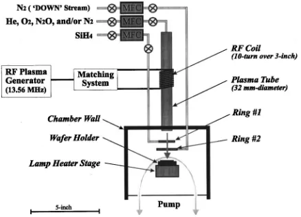
Process steps were performed in a multichamber ultrahigh-vacuum 共UHV兲 system, which is shown in Fig. 1,
and contains: 共i兲a load-lock chamber, 共ii兲 a remote plasma processing chamber for oxidation, nitridation, and bulk film deposition, 共iii兲 a rapid thermal annealing 共RTA兲 chamber,
共iv兲 a buffer chamber, and 共v兲 a surface analysis chamber with Auger electron spectroscopy 共AES兲. Remote plasma processing30 offers wide range process capabilities for di-electric applications; oxidation, nitridation, and oxide, nitride and oxynitride alloy deposition 共see Fig. 2兲. There are two ways to implement remote plasma processing; 共i兲 ‘‘UP’’ stream processes in which all process gases go through the plasma tube and are remotely excited by the rf plasma, e.g., O2/He for oxidation of Si surfaces and N2/He plasma
nitri-dation of Si surfaces and 共ii兲‘‘DOWN’’ stream processes in which one, or more of the process gases is injected from a FIG. 1. Process sequence for two-step interface formation共process I兲:共i兲 O2/He plasma oxidation of Si surface followed by共ii兲N2/He plasma
nitri-dation at 0.3 Torr,共iii兲bulk SiO2film deposition, and共iv兲postoxide
depo-sition anneal.
FIG. 2. Top-view of UHV multichamber system:共i兲load lock,共ii兲remote plasma processing,共iii兲rapid thermal annealing,共iv兲surface analysis, and
gas dispersal ring, and therefore are not directly excited by the remote plasma, e.g., SiO2 deposition and Si3N4 deposi-tion processes in which SiH4 is injected through the down-stream dispersal ring.
The Si共100兲substrates used in these studies were prepared by first growing 10 nm of sacrificial oxide on a chemically clean and HF rinsed surface. This was accomplished by dry oxidation in O2 at 900 °C. Prior to the different nitridation
processing steps described below, the sacrificial oxide was removed by rinsing in dilute HF before loading into the sys-tem described in Sec. II A.
B. Nitridation processings
1. Process I: O2/He plasma oxidation of Si followed by N2/He plasma nitridation
This process for incorporation nitrogen at the Si–SiO2
interface includes two plasma processing steps performed at a substrate temperature of 300 °C: 共i兲 a remotely plasma-assisted O2/He oxidation of the Si surface at 300 °C to form
a ⬃0.5–0.6-nm-thick superficial oxide, followed by 共ii兲 a remotely activated N2/He plasma nitridation to incorporate
the nitrogen atoms at the Si–SiO2 interface. Figure 1
illus-trates this process sequence for interface nitridation. The oxi-dation共the first step兲creates a device quality Si–SiO2
inter-face and grows ⬃0.6 nm of SiO2, and the nitridation 共the
second step兲 controls the degree of nitrogen at the Si–SiO2
interface by varying the N2/He plasma exposure time. For
the oxidation process, an O2/He mixture with flow rates of
20 sccm for O2 and 200 sccm for He is injected through the
plasma excitation tube of the processing system共UP stream兲. The process pressure and rf power at 13.56 MHz were 0.3 Torr and 30 W, respectively. For the nitridation process, the N2/He discharge was initiated using flows of 60 sccm N2and 160 sccm He; the process pressure was 0.3 Torr; the rf power was 30 W. The bulk SiO2 layer was formed by RPECVD with 2%-SiH4 in He and O2/He gas mixtures as the
respec-tive source gases for Si and O. The O2/He mixture was
in-jected through the rf plasma region, but the SiH4 gas was
injected DOWN stream through a showerhead dispersal ring outside of the plasma excitation region. The gas flow rates and process pressure were adjusted to prevent back stream-ing of the SiH4 into the plasma generation region of the
reactor. The gas flow ratios for O2, He, and 2%-SiH4 in He
were, respectively, 20, 200, and 10 sccm. Postoxide deposi-tion annealing was performed in the on-line rapid thermal annealing共RTA兲chamber at 0.3 Torr at 900 °C for 30 s in a He ambient. The postoxide deposition anneal reduces chemi-cal and structural strain in the bulk film and at the Si–SiO2
interface.31,32This process sequence can be characterized as an ‘‘oxide first’’ process, whereas processes II and III are each ‘‘nitride first’’ processes.
2. Process II: N2/He plasma nitridation of Si
This nitride first process sequence uses the second, third, and fourth steps that have been described in the preceding section to achieve a nitrided interface; i.e., the N2/He
plasma-assisted nitridation at 300 °C, bulk SiO2 deposition
at 300 °C, and RTA at 900 °C. Specifically, this process is a remote plasma nitridation of the Si surface, and does not involve an oxidation step prior to the nitridation.
3. Process III: Si3N4film deposition on Si
A third way to confine nitrogen at the Si–SiO2interface is
two-step nitride first deposition process sequence: 共i兲a thin Si3N4deposition by RPECVD directly onto the Si substrate,
followed by共ii兲a bulk SiO2deposition by RPECVD onto the
deposited nitride interfacial layer共Fig. 3兲. Both process tem-peratures were 300 °C. For the Si3N4 deposition,33the flow
rates for N2, He, and 2%-SiH4 in He were 60, 200, and 10
sccm, respectively. For the SiO2 deposition, the flow rates
for O2, He, and 2%-SiH4 in He were 20, 200, and 10 sccm,
respectively. As in process II, the 2%-SiH4 in He was
in-jected DOWN stream from the plasma region through a showerhead injector, and the other process gases were in-jected UP stream through the plasma tube and subin-jected to direct plasma excitations. Both depositions were performed at an rf power of 30 W. The process pressures were 0.2 and 0.3 Torr, for the Si3N4 and SiO2 depositions, respectively. Postdeposition annealing was carried out in the on-line RTA chamber at 900 °C at 0.3 Torr for 30 s in He ambient.
C. Interface analysis
The substrates used in these studies were 50-mm-diam
n-type 共phosphorus doped兲 Si共100兲 with a resistivity of 0.02–0.045 ⍀cm (⬃5⫻1017 cm⫺3). For each of the pro-cesses discussed below the Si substrate preparation was the same. After a conventional wet chemical RCA clean, a 10-nm-thick sacrificial oxide was grown in dry O2 in a
conven-tional thermal furnace at 900 °C. Immediately before loading the sample into the multichamber processing system, the sac-rificial oxide was removed by etching in a dilute HF共1 wt %兲 solution, rinsed in a running distilled共DI兲water for 20 s, and then dried in flowing N2.
AES was performed in the on-line analysis chamber of the multichamber system to quantify the initial stages of oxidation/nitridation of the Si surface using a 3 keV electron beam. Secondary ion mass spectrometry 共SIMS兲 analyses
were done at Evans East, NJ, using CsN⫹ ions for depth profiling of the interfacial nitrogen. Nuclear reaction analysis
共NRA兲 was carried out at the IBM T.J. Watson Research Center, NY, for nitrogen concentration calibration.34
D. Device fabrication and electrical characterization For device fabrication and electrical characterization stud-ies, the substrates were 50-mm-diam phosphorus-doped
n-type Si共100兲 with a resistivity of 0.02–0.045 ⍀cm (⬃5
⫻1017cm⫺3) and boron-doped p-type Si共100兲with a
resis-tivity of 0.05–0.07 ⍀cm (⬃5⫻1017 cm⫺3). The use of
heavily doped Si wafers reduces spreading resistance and thereby minimizes parasitic series resistance, and accompa-nying voltage drops in the bulk Si. MOS capacitors with field oxide isolation structures were made on Si共100兲wafers using conventional photolithography processes. All devices studied have an area of 10⫺4 cm⫺2, i.e., the linear dimensions of these devices were 100m by 100m.
For the electrical characterization,共i兲gate currents or cur-rent density versus gate voltages共I – V or J – V兲 characteris-tics and 共ii兲 capacitance versus gate voltage共C – V兲 charac-teristics were measured. The C – V measurements were used to determine an equivalent oxide thickness, and to estimate densities of interfacial defects, both interface traps, Dit, and
fixed positive charge. For the I – V or J – V measurements, the gate electrode was biased positively共substrate injection mode兲for the n-type Si in order to maintain the substrate in an accumulation state.
III. RESULTS
A. Process I: O2/He plasma oxidation of Si followed by N2/He plasma nitridation
Interfacial oxidation/nitridation of the Si surface produces a device quality interface using O2/He remote plasma
oxida-tion process28and then incorporates nitrogen at the Si–SiO2 interface using the N2/He remote plasma nitridation at 0.3 Torr. The first step, O2/He plasma-assisted oxidation process has three functions; it 共i兲 removes carbon contamination from the Si surface,17,28共ii兲creates a device quality Si–SiO2 interface, and共iii兲grows⬃0.5–0.6 nm of SiO2 as shown in
Fig. 4. Figure 4 共i兲shows a differential AES spectrum from the Si substrate after the RCA clean, that reveals an ⬃ 0.7-nm-thick chemical oxide and carbon contamination 共CKLL feature at ⬃272 eV兲 on the Si. This chemical oxide was removed using a 1 weight 共wt兲% HF:H2O solution, which
did not completely remove the carbon contamination, see Fig. 4 共ii兲. Additionally, the carbon contamination did not disappear following heating to 300 °C in the UHV-compatible chamber as shown in Fig. 4 共iii兲. However as shown in Fig. 4共iv兲, the O2/He plasma reduced the carbon
contamination level, consistent with the results presented in Refs. 17 and 28. If residual carbon was at the Si–SiO2
inter-face at a level⬎⬃0.5 at. %, then it would be observable by AES since the oxide thickness of ⬃0.5 nm is less than the electron escape depth of the electrons associated with the CLVV Auger feature共⬃1 nm兲. Therefore it is concluded that
the O2/He plasma removed carbon contamination from the Si
surface 共Si–SiO2 interface兲 to the level of AES detection
limit,⬃0.5 at. %, and formed a superficial SiO2 layer on the Si.
The second step, N2/He plasma nitridation of the superfi-cial oxide was studied using on-line AES. Figure 5 shows differential AES spectra for共i兲15 s O2/He plasma oxidation of the Si surface followed by共ii兲–共v兲N2/He plasma
nitrida-tion treatments ranging from 30 to 120 s. The incorporanitrida-tion of nitrogen atoms is reflected in the evolution of NKLL AES peak at⬃379 eV. The intensity of NKLLincreased monotoni-cally as the exposure time to the N2/He plasma postoxidation
treatment was increased. This demonstrated that longer ex-FIG. 4. On-line differential AES spectra of Si surfaces after共i兲RCA clean, 共ii兲rinse in 1 wt % of HF,共iii兲300 °C heating for 10 min in UHV system, and 共iv兲a 5 s O2/He plasma oxidation of Si surface. The electron beam
energy was 3 keV.
FIG. 5. On-line AES spectra using a 3 keV electron beam. Differential spectra are after共i兲a 15 s O2/He plasma oxidation of Si surface followed by
共ii兲–共v兲N2/He plasma nitridation of the superficial oxide for 30, 60, 90, and
posure times resulted in increased nitrogen incorporation ei-ther at the Si–SiO2interface or in the bulk of⬃0.6-nm-thick
oxide layer.
The following experiments established that the nitrogen incorporation was at the Si–SiO2 interface; i.e., at the
met-allurgical boundary between the Si substrate and the SiO2
layer. The top AES trace in Fig. 6 共sample A兲is after 15 s O2/He plasma oxidation of the Si surface which formed an ⬃0.6-nm-thick oxide. There is no detectable NKLL feature at
⬃379 eV. Following the 60 s N2/He plasma exposure
pro-duced a weak NKLL feature as is evident in the middle AES trace in Fig. 6共sample B兲. The wafer was then removed from the UHV system, etched in a very dilute HF 共0.5 wt %兲 to remove most of the thin oxide layer. The sample was rein-serted into the UHV system, annealed in He at 900 °C for 30 s in the on-line RTA module, and then analyzed again using the on-line AES. The AES spectrum is shown in the bottom trace of Fig. 6共sample C兲. A comparison between the Si–O
共at⬃76 eV兲and Si–Si共at⬃91 eV兲traces of the SiLVVAES spectra between the middle and lower traces of Fig. 6 shows the oxide thickness is significantly reduced by the ex situ HF etching from ⬃0.6 nm to less than 0.4 nm; however, the weak NKLL feature remains almost unchanged. This estab-lishes that the post oxidation nitridation processing intro-duces nitrogen atoms at the Si–SiO2 interface.
SIMS analyses have been used to quantify the nitrogen content at the interface. Four samples with different nitrida-tion times from 30 to 120 s were studied. Each sample was subjected to 共i兲 15 s O2/He plasma oxidation followed by
interface nitridation, 共ii兲bulk oxide deposition by RPECVD
共⬃7.0 nm thick兲followed by 共iii兲 on-line 900 °C postoxide deposition anneal. Based on a standard reference sample at Evans East, NJ, the interfacial nitrogen concentration共areal density兲 has been determined by integration of the SIMS depth profile. This demonstrated that the 90 s N2/He
nitrida-tion incorporated approximately one monolayer of nitrogen
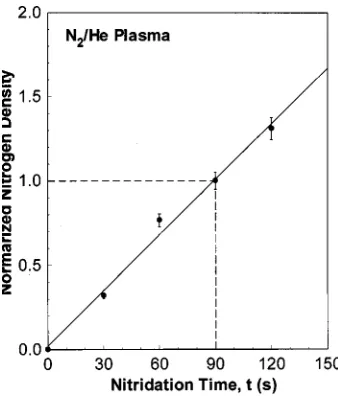
(⬃7⫾1⫻1014cm⫺2) at the interface. NRA studies sup-ported the SIMS analysis and data reduction by showing that the 90 s N2/He plasma nitrogen process incorporated ⬃8.4 ⫾1⫻1014 cm⫺2 nitrogen atoms at the interface.34 Figure 7 presents the normalized integrated areal densities with re-spect to the 90 s nitridation data as a function of nitridation time, which show interfacial nitrogen concentration in-creased linearly with nitrogen plasma exposure time.
This interfacial nitridation process has been used in the fabrication of MOS capacitors with thickness range from 4.5
共FN tunneling region兲down to 2.0 nm thick共direct tunneling region兲 on n-Si共100兲 substrates using aluminum 共Al兲 gate electrodes. Figure 6 includes a series of J – V traces for de-vices with Al gate electrodes and a 4.5-nm-thick gate oxide on n-Si共100兲 wafers. The gate electrode was biased posi-tively so that gate current flowed from the substrate to the gate electrode in the so-called substrate injection mode. The sequence of traces in this figure demonstrates the effect of the interfacial nitrogen is to reduce the tunneling current in the FN region共Fig. 8兲. This reduction is not due to an oxide thickness change and/or a flat band voltage shift that results from incorporation of nitrogen at the Si–SiO2interface.
Fig-ure 9 displays that high frequency and quasistatic C – V mea-surements for devices fabricated: 共i兲 without interface nitri-dation, and 共ii兲 with the 90 s N2/He plasma nitridation
processes. The two C – V curves were essentially identical. This means that the effective oxide thickness and flat band voltage are the same with and without the interfacial nitro-gen. Therefore, the leakage current reductions in the FN re-gion are not due to differences in the oxide thickness or flat band voltage shifts. In this regard, it is important to note that interfacial nitridation would not change the physical thick-ness of the dielectrics by more than 0.1 nm, which falls with in the uncertainty of the capacitance determination of oxide equivalent dielectric thickness. A model calculation showed that a 0.1 nm difference in physical thickness cannot account FIG. 6. On-line differential AES spectra using a 3 keV electron beam.
Dif-ferential spectra are after共i兲a 15 s O2/He plasma oxidation of Si surface
共sample A兲followed by共ii兲60 s N2/He plasma postoxidation nitridation
共sample B兲, and共iii兲ex situ HF dip and on-line RTA at 900 °C共sample C兲.
for the differences in current between the first and last two traces in Fig. 4. In addition, the positions of the flat band voltage, with respect to each other, as well as their absolute positions are consistent with fixed positive charge densities
⬍1011cm⫺2, independent of the interface nitridation.
B. Process II: N2/He plasma nitridation of Si
This is a direct nitridation of the Si surface using a re-motely activated N2/He plasma. Figure 10 shows initial stages of the N2/He plasma nitridation of the Si surface as studied by on-line AES. The oxygen AES features共at⬃510 eV兲was not observed. The oxygen contamination was well
below the AES detection limit共⬃0.5 at. %兲. However, a car-bon AES feature at ⬃272 eV was observed. This means, unlike the O2/He plasma process, the N2/He plasma
nitrida-tion was not effective in removing carbon contaminanitrida-tion from the Si surface, see Fig. 5 for this comparison.
Using this AES intensity ratio and the following equation, we can then estimate a thickness of nitrided layer on the Si surface:
tSiN⫽ln
冉
1⫹I°Si–Si I°Si–NISi–N
ISi–Si
冊
, 共1兲
where, tSiN⫽nitride thickness共nm兲,⫽electron escape depth
共attenuation length兲; ⬃0.6 nm, ISi–No ⫽Si–N signal from a thick Si3N4 surface共reference sample兲, I°Si-Si⫽Si-Si signal
from a clean Si surface共reference sample兲, ISi–Si⫽SiLVV sub-strate signal at ⬃91 eV from a thin nitride on the Si and
ISi–N⫽SiLVV nitrogen shifted signal at ⬃83 eV from a thin nitride on the Si. Figure 11 shows the thickness of the nitride layer, tSiN, as a function of nitridation time. The nitridation
rate is initially fast and then tends to saturate. This indicates that the thin nitrided layer on the Si prevents the further nitridation of the Si surface so that the process is in effect self-limiting. The nitride thickness is fit by the following relationship for first-order reaction kinetics:
tSiN⫽0.69兵1⫺exp共⫺0.011tN兲其 共nm兲, 共2兲 where, tSiN⫽nitride thickness 共nm兲and tN⫽nitridation time
共min兲. The prefactor term 共in nm兲 is equivalent to approxi-mately 1.5 molecular layers of Si3N4, and the exponential
prefactor term, 0.011共in min兲is the inverse of the effective rate constant for the formation of the nitride layer. This fit first-order kinetics suggests that the nitridation process slows down considerably after about one to two monolayers of nitride are formed on the Si substrate.
We have analyzed the SIMS data to determine the inter-facial nitrogen areal density. We prepared four samples with FIG. 8. Substrate injection mode 共gate-electrode biased positively兲 J – V
traces for devices with 4.5-nm-thick gate oxides on n-Si共100兲. These traces demonstrate the effect of increasing interfacial nitrogen up the one mono-layer level in reducing tunnel currents in the FN regime. The gate electrode was Al.
FIG. 9. High-frequency 共1 MHz兲and quasistatic C – V measurements of devices in Fig. 8 with共i兲without nitridation共no nitrogen at interface兲, and 共ii兲with a 90 s nitridation process. The gate electrode was Al.
FIG. 10. On-line differential AES spectra using a 3 keV electron beam following N2/He plasma nitridation of a Si surface for共i兲30,共ii兲60,共iii兲90,
different N2/He plasma nitridation times from 30 to 120 s,
and completed the test structures with the REPCVD deposi-tion of ⬃7.0-nm-thick bulk oxide film followed by 900 °C postoxide deposition on-line anneal in an inert ambient. Fig-ure 12 displays the nitrogen SIMS depth profile using CsN⫹ ions which shows that as the N2/He plasma exposure time
was increased, the peak concentration of nitrogen at the Si–SiO2 interface was increased. Using this SIMS data and
the standard sample at Evans East, NJ, the equivalent areal density of nitrogen atoms at the interface is calculated. Fig-ure 13 compares the areal density of共i兲process II, the direct N2/He plasma nitridation of the Si surface for 30–120 s and 共ii兲 process I, the two-step interface formation, the O2/He
plasma oxidation of the Si surface followed by the N2/He
plasma nitridation for 45 and 90 s data. For the process we
have designated as process I, i.e., the two-step interface pro-cess, the areal density increased linearly with nitridation time
共see Fig. 7兲, whereas for the direct N2/He nitridation of the
Si, the process we have designated as process II, the nitrogen areal density at the interface exhibited a saturation behavior due to a self-limiting process for nitride layer growth. The interfacial nitrogen incorporation of the direct nitridation process共process II兲is faster and incorporates more nitrogen initially than the two-step interface formation process 共 pro-cess I兲, and then tends to saturate after the formation of about one to two monolayers are formed.
We have fabricated the MOS capacitors for the electrical characterization of this direct interfacial nitridation process-ing. The test devices structures were prepared in the follow-ing way: test device共i兲: O2/He plasma oxidation of the Si⫹ RPECVD SiO2 deposition from O2/He and SiH4, test device
共ii兲: 30 s N2/He nitridation of the Si⫹RPECVD SiO2 from O2/He and SiH4 and test device共iii兲: 90 s N2/He nitridation of the Si⫹RPECVD SiO2 from O2/He and SiH4. The total
equivalent oxide thickness, as determined from C – V mea-surements, was 3.8⫾0.1 nm for all samples. All samples were subjected to on-line postoxide deposition anneal at 900 °C at 0.3 Torr for 30 s in He ambient.
Similar to the two-step interface formation 共process I兲, which was demonstrated to reduce tunneling in the FN re-gime 共see Fig. 8兲, a reduction of tunnel current in the FN regime was also observed for the devices with the nitrided interfaces. Figure 14 displays current density plotted as func-tion of gate voltage for共i兲no nitrogen atoms at the Si–SiO2
interface, 共ii兲 ⬃1.1⫻1015 cm⫺2 nitrogen in the interfacial nitride layer, and 共iii兲 ⬃1.6⫻1015cm⫺2 nitrogen in the in-terfacial nitride layer. However, as more nitrogen was incor-porated in the interfacial layer, there was a large flat band voltage shift in the negative direction, as determined from
C – V data. Figure 15 shows the flat band voltage for 共i兲 a reference oxide sample with no nitrogen at the interface, and FIG. 11. Thickness of the nitrided layer in Fig. 10 as a function of N2/He
plasma exposure time.
FIG. 12. SIMS depth profiles of four different interfacial nitridation times; 共i兲30,共ii兲60,共iii兲90, and共iv兲120 s. Total oxide thickness was⬃6 nm. The secondary ions for SIMS detection were CsN⫹.
FIG. 13. Comparisons of areal density from SIMS data vs time for共i兲N2/He
plasma nitridation of Si surface共process II兲and共ii兲two-step interface for-mation process of O2/He plasma oxidation of Si surface followed by N2/He
for two samples with interface nitridation time of 共ii兲 30 s and共iii兲and 90 s. Figure 16 replots the FN region tunneling currents versus gate voltage minus flat band voltage (Vg
⫺Vfb). Although some reduction in FN tunneling current
was observed as function of increasing (Vg⫺Vfb), the reduc-tions of tunneling current for this direct nitridation process were not as large as compared with those of the two-step interface formation process 共process I兲.
C. Process III: Si3N4film deposition directly onto Si The third technique for interfacial nitridation is a direct deposition by 300 °C RPECVD of a Si3N4 film onto the Si
surface. Figure 17 shows AES traces for initial stages of
Si3N4 deposition on the Si surface. Similar to the direct
N2/He plasma nitridation of the Si surface 共process II兲, the
Si3N4 deposition process was not effective in removing
car-bon contamination from the Si surface as evidenced by the CKLL AES feature is at⬃272 eV. After a 180 s deposition, the CKLLAuger signal was no longer observed; however, this is attributed to the carbon being buried at the Si3N4/Si inter-face. As shown in Fig. 17, after 180 s of deposition, the nitride layer thickness was larger than the AES electron es-cape depth for electrons from the SiLVV transitions. In addi-tion, the signal associated with CKLLAES electrons was sig-nificantly attenuated. Using these Auger intensities and Eq.
共1兲, the nitride layer thickness has been determined. Figure 18 illustrates that the nitride thickness increased as linear FIG. 14. Substrate injection mode 共gate-electrode biased positively兲J – V
traces for 3.8-nm-thick gate oxide on n-Si共100兲. These are plotted as a function of gate voltage. These traces demonstrate the effects of interfacial nitrogen reducing tunnel currents in the FN region. The gate electrode was Al.
FIG. 15. Flat band voltage shift as a function of interfacial nitridation time. The flat band voltage was determined by analysis of high frequency C – V date. The gate electrode was Al.
FIG. 16. J vs (Vg⫺Vfb) traces in the substrate injection mode for devices
with for共i兲no nitrogen at interface,共ii兲30 s and共iii兲90 s direct interfacial nitridation interfacial nitridation. The equivalent oxide共electrical兲thickness was 3.8 nm for all three samples. Gate electrode was Al.
FIG. 17. On-line differential AES spectra using a 3 keV electron beam. The spectra are Si3N4thin film depositions onto a Si surface. Deposition times
function deposition time as expected for deposition process. The thickness of one molecular Si3N4 is approximately 0.42
nm, as estimated from the density of Si3N4, so that a 60 s
deposition forms approximately 1.4 molecular layers of sili-con nitride.
MOS capacitors were fabricated and used for electrical characterization. The test devices included the following di-electric structures: test device共i兲: O2/He plasma oxidation of
the Si⫹300 °C RPECVD SiO2 deposition from O2/He and
SiH4, test device 共ii兲: ⬃one molecular layer of deposited
Si3N4 共⬃0.4 nm兲 on the Si⫹300 °C RPECVD SiO2 from
O2/He and SiH4and test device共iii兲:⬃two molecular layers
Si3N4 共⬃0.8 nm兲 on the Si⫹300 °C RPECVD SiO2 from O2/He and SiH4. All of the stacked dielectrics were annealed at 900 °C at 0.3 Torr for 30 s in He in the on-line RTA chamber. The total ‘‘equivalent’’ oxide thickness was main-tained ⬃4.3⫾0.1 nm for all samples as determined from
C – V measurements. This was achieved by systematically
varying the thickness of the deposited oxide layers. Assum-ing that the dielectric constant of the nitride layer is approxi-mately twice that as SiO2, this means that the nominal
‘‘physical’’ thicknesses of the dielectric layers in these de-vices were: test device共i兲4.3 nm, test device共ii兲4.5 nm, and test device共iii兲4.7 nm. The deposition time for the SiO2was
adjusted to compensate for the nitride layer thickness, so that test device共iii兲had the shortest SiO2 deposition time.
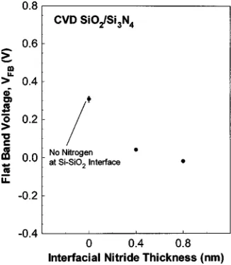
Figure 19 shows high-frequency C – V traces for the three samples in both sweep directions, i.e., from accumulation to depletion and back to accumulation. Due to the fast sweep-ing gate bias, the C – V traces exhibited a deep depletion effect. The depletion layer width becomes wider than in mal equilibrium and the capacitance decreases below its ther-mal equilibrium saturation value.35,36 No hysteresis effects were observed in the steep part of the C – V trace, indicating a relative low density of slow oxide or interface traps. How-ever, we did observe a large negative flat band voltage shift that increased with increasing interfacial Si3N4 layer
thick-ness. Figure 20 plots the flat band voltage as a function of the thickness of the interfacial Si3N4layer. The 0.4- and
0.8-nm-thick Si3N4 layers correspond respectively to approximately
one- and two-molecular layers of Si3N4 at the interface.
Un-like the two-step interfacial oxidation/nitridation共process I兲, the interfacial deposited Si3N4 layer produced a large flat
band voltage shift indicating a high density of fixed positive charge,⬃1012cm⫺2.
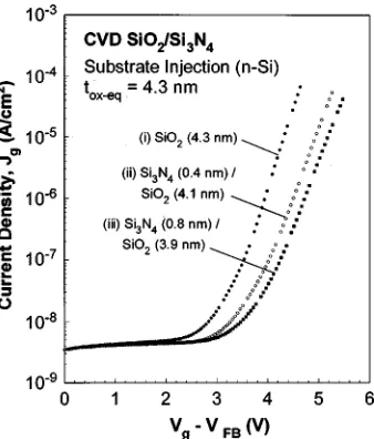
Reductions in tunnel current were also observed when one- to two-molecular layers of Si3N4 were interposed
be-tween the Si substrate and the deposited thick SiO2. Figure
21 shows current density versus gate voltage-flat band volt-age traces for the three test devices identified above with an oxide equivalent thickness of 4.3⫾0.1 nm as determined FIG. 18. Thickness of deposited nitride layer in Fig. 17 as a function of
deposition time.
FIG. 19. High-frequency共1 MHz兲C – V traces共in both directions兲for de-vices with共i兲no nitrogen,共ii兲one and共iii兲two molecular layers of Si3N4at
the interface. The equivalent oxide共electrical兲thickness was 4.3 nm for all samples. The gate electrode was Al, and the arrows indicate the sweep directions.
from accumulation bias capacitance. The tunneling current in Fig. 21 decreased as thickness of Si3N4layer at the interface
increased. When we plotted the current density versus gate voltage minus the flat band voltage (Vg⫺Vfb), the leakage
current reduction was more pronounced than for process I, compare Figs. 8 and 21. However, it is difficult to make direct quantitative comparisons between the J – V traces for the two interface nitridation processes discussed above. In particular even though the reductions in J with increasing nitridation are comparable, the areal densities of nitrogen atoms differ by factors of approximately ten for the 0.4-nm-thick nitride film and twenty for the 0.8-nm-0.4-nm-thick nitride film when compared to the monolayer nitridation of process I.
Finally, Fig. 22 displays high frequency and quasistatic
C – V traces for the same three test devices of this section.
Interfacial nitridation via Si3N4 deposition reduced the tun-neling currents but the interfacial defect density increased significantly, Ditlevels determined by conventional analysis
of high frequency and quasistatic C – V traces, increased from the mid 1010cm⫺2 range for the devices fabricated by process I, to more than 15⫻1011 cm⫺2 for the devices with deposited nitride layers shown in Fig. 22. Fixed positive charge, determined by shifts of the C – V traces to more negative voltages increased by more than an order of mag-nitude into the 1012cm⫺2 range. This increased density of interface state has been shown to effect the channel mobili-ties in both n- and p-channel MOSFET devices.37,38 In particular Misra et al.37have shown that peak values of elec-tron mobility are reduced by a factor of 2 in the n-channel MOSFET’s, whereas peak values of the hole mobility are reduced by more than a factor of 10–20 in p-channel MOS-FETs. These results indicate that charged defects associated with direct deposition of Si3N4 onto Si are associated with
donor-like defects that reside in the lower half of the silicon band gap.
IV. DISCUSSION
We have investigated three different ways of incorporat-ing nitrogen at the Si-dielectric interface: process 共I兲O2/He
plasma oxidation of the Si surface followed by the N2/He
plasma nitridation, process 共II兲N2/He plasma nitridation of
the Si surface, and process共III兲Si3N4 film deposition on the
Si surface. Based on significant negative shifts of the flat band voltage that increased as the nitrogen incorporation at the interface increased, we have demonstrated the processes labeled 共II兲 and共III兲 degraded device performance through the development of large densities of fixed positive charge in the dielectric in the immediate vicinity of the Si-dielectric interface. All three processes resulted in decreases in FN tunneling current, however, the shifts in flat band voltage, as well as increases in interfacial defects, Dit, render processes 共II兲and共III兲useless for advanced device structures.
It is necessary to explain why postoxidation, interface ni-tridation of process 共I兲 and the direct oxidation/nitridation using N2O,18each of which incorporates monolayer levels of
nitrogen at the interface improve device performance and reliability, whereas higher concentrations of nitrogen as in processes 共II兲 and 共III兲 clearly degrade interface electrical properties. The experiments reported in Refs. 37 and 38, have shown that the problem is not with the RPECVD film itself, since insertion of as little as 0.5 nm of SiO2 between
the Si substrate and the deposited nitride restores electrical performance and reliability to values comparable or exceed-ing those of devices with optimized oxide dielectrics of the same equivalent thickness.
Lucovsky and co-workers have found that the average bonding coordination Navat the dielectric-Si interface is key
to understanding the origin of interfacial defect generation.39 Reference 39 has extended constraint theory, originally pro-posed by Phillips40to explain the ease of glass formation in FIG. 21. J vs (Vg⫺Vfb) traces in the substrate injection mode for devices of
Fig. 19 with 共i兲no nitrogen at the interface, and 共ii兲one and 共iii兲 two molecular layers of Si3N4 at interface. The equivalent oxide 共electrical兲
thickness was 4.3 nm for all samples. The gate electrode was Al.
FIG. 22. High-frequency共1 MHz兲and quasistatic C – V measurements for devices in Fig. 19 with共i兲no nitrogen,共ii兲one and共iii兲two molecular layers of Si3N4at interface. The equivalent oxide共electrical兲thickness was 4.3 nm
materials such as As2S3, GeSe2, and SiO2, to the interface
between noncrystalline dielectrics and semiconductor. Phil-lips demonstrated that the condition for ideal glass formation corresponded to matching bonding constraints per atom in
the context of valence forces to the network
dimensionality.40This demonstrated that ideal random cova-lent networks, which form the basis for glass formation oc-curred when Nav was in a range between 2.4 and 2.7. In
extending the constraint theory formulation, Lucovsky et al. focused on differences between interface nitridation to estab-lish a link the relationship between average interfacial coor-dination and defect properties.39Results presented in Ref. 41 initially extended the Phillips theory40 bulk glasses to thin films, suggesting that an average coordination per atom of approximately three separates device quality thin films from films with increasing defect densities. The results presented in Ref. 39 confirmed that Nav⬃3 also provides a demarca-tion value between device quality and highly defective inter-faces, with defect values of about 5⫻1010cm⫺2defining this boundary. Applying the model of Ref. 39, Table I includes a calculation of the Nav for interfaces studied in this article.
The interfaces that show excellent electronic properties, Si–SiO2, and monolayer nitrided Si–N–SiO2formed by
pro-cess 共I兲, have Nav values of 2.8 and 2.9, respectively,
whereas the interface formed by processes共II兲and共III兲, have values in excess of 3, consistent with the criterion developed in Ref. 39. For completeness the table also demonstrates that the insertion of about one and a half molecular layers of SiO2
共⬃0.5–0.6 nm兲yields a value of Nav⬍3 in accordance with the significant improvement in electrical properties that has been reported.37,38
V. CONCLUSIONS
We have demonstrated three different plasma-assisted in-terface nitridation processes: 共i兲 process I - O2/He plasma
oxidation of the Si surface followed by N2/He plasma
nitri-dation, 共ii兲 process II - N2/He plasma nitridation of the Si
surface, and共iii兲process III - deposition Si3N4film on the Si
surface. Process I is an oxide-first process, while processes II and III are both nitride first processes. For process I, the first step, the 300 °C remote plasma assisted O2/He oxidation of
the Si surface reduces significantly/removes carbon contami-nation, creates a device quality Si–SiO2interface, and forms ⬃0.6 nm of SiO2 which served as a substrate for the
RPECVD deposition of dielectric films. The second step, a
300 °C remote plasma assisted N2/He plasma nitridation
controls the degree of the nitrogen incorporation at the Si–SiO2interface. AES studies of etched back surfaces
con-firmed the nitrogen was localized at the interface, and SIMS and NRA analysis established that a 90 s plasma exposure time incorporated approximately one monolayer of interfa-cial nitrogen (⬃7⫾1⫻1014 cm⫺2). This monolayer nitro-gen incorporation reduced tunneling current direct42and FN and tunneling regimes.
Consider next process II, the direct nitridation of a Si surface. Unlike process I, the direct nitridation of Si using N2/He plasma process did not remove carbon contamination from the Si surface. Monitoring nitrogen content as a func-tion of nitridafunc-tion time by AES established that this interfa-cial nitridation process was effectively self-limiting, slowing down considerably after about two monolecular of nitride formation. The nitridation process for the first molecular layer was very fast, and in contrast to process I, it is more difficult to control incorporation of nitrogen in the range ex-tending up to about one monolayer. The electrical properties of this interface as monitored by C – V measurements were degraded as indicated by flat band voltage shifts in the nega-tive direction that increased with increasing nitridation time. In addition, reductions in tunneling current in the FN regime were reduced with respect to those obtained with process I.
Process III was the direct deposition by RPECVD at 300 °C of Si3N4 onto the Si surface. This process also did
not remove carbon contamination. As in a typical CVD pro-cess, the amount of nitrogen, or equivalently, thickness of the nitrided layer, increased linearly with increasing deposi-tion time. Similar to process II the Si–Si3N4 interface
dis-played a high defect density, as reflected in a large negative flat band voltage shift. However, the reductions in tunneling current as function of the voltage drop across the dielectric layer (Vg⫺Vfb) were comparable to those obtained with
monolayer nitridation in process I.
Therefore, among the three interfacial nitridation pro-cesses, process I, the two-step interface formation process displayed the best electrical results. This was consistent with the predictions of constraint theory as applied to crystalline-Si dielectric interfaces in Ref. 39.
ACKNOWLEDGMENTS
This work is funded in part by the Office of Naval Re-search共ONR兲, the National Science Foundation-Engineering Research Center 共NSF-ERC兲, and the Semiconductor Re-search Corporation 共SRC兲. The authors also would like to thank Dr. D. Buchanan and Dr. S. Cohen for nuclear reaction analysis.
1T. Hori and H. Iwasaki, IEEE Electron Device Lett. EDL-10, 64共1989兲. 2H. Fukuda, M. Yasuda, T. Iwabuchi, and S. Ohno, IEEE Electron Device
Lett. EDL-12, 587共1991兲.
3
J. Ahn, J. Kim, G. Q. Lo, and D.-L. Kwong, Appl. Phys. Lett. 60, 2809
共1992兲.
4Z. Liu, H.-J. Wann, P. K. Ko, C. Hu, and Y. C. Cheng, IEEE Electron
Device Lett. EDL-13, 519共1992兲.
5H. S. Momose, T. Morimoto, Y. Ozawa, K. Yamabe, and H. Iwai, IEEE
Trans. Electron Devices ED-41, 546共1994兲. TABLEI. Average bonding coordination, Nav, at Si-dielectric interfaces.
Si-dielectric interface system Average coordination (Nav)
Si–SiO2共1.5 molecular layers兲 2.8
Si–Si3N4共1.5 molecular layers兲 3.5
Si–Si3N4(t)-SiO2
t⫽nitride layer thickness t⫽0.4 nm, 3.3
t⫽0.8 nm, 3.4
Si–N共1.0 monolayer兲-SiO2 共1.5 molecular layers兲
2.9
Si–SiO2(t)-Si3N4 t⫽0.5 nm, 2.9
6T. Hori and H. Iwasaki, Proc. SPIE 1189, 176共1989兲. 7
G. Q. Lo, W. C. Ting, D. K. Shih, and D.-L. Kwong, Appl. Phys. Lett. 55, 979共1990兲.
8Z. H. Liu, J. T. Kirk, H. J. Wann, P. K. Ko, C. Hu, and Y. C. Cheng,
Tech. Dig. Int. Electron Devices Meet. 625共1992兲.
9
Y.-S. Kim, Y. Okada, K.-M. Chang, P. J. Tobin, B. Morton, H. Choe, M. Bowers, C. Kuo, D. Chrudimsky, S. A. Ajuria, and J. R. Yeargain, IEEE Electron Device Lett. EDL-14, 342共1993兲.
10L. K. Han, D. Wristers, J. Yan, M. Bhat, and D.-L. Kwong, IEEE
Elec-tron Device Lett. EDL-16, 319共1995兲.
11
M. Bhat, D. J. Wristers, L.-K. Han, J. Yan, H. J. Fulford, and D.-L. Kwong, IEEE Trans. Electron Devices EDL-42, 907共1995兲.
12H. Hwang, W. Ting, D.-L. Kwong, and J. Lee, Tech. Dig. Int. Electron
Devices Meet. 421共1990兲.
13
G. Q. Lo, W. Ting, J. Ahn, and D.-L. Kwong, Dig. Tech. Papers Symp. VLSI Tech. 43共1991兲.
14Z.-Q. Yao, H. B. Harrison, S. Dimitrijev, D. Sweatman, and Y. T. Yeow,
Appl. Phys. Lett. 64, 3584共1994兲.
15C. T. Liu, E. J. Lloyd, Y. Ma, M. Du, R. L. Opila, and S. J. Hillenius,
Tech. Dig. Int. Electron Devices Meet. 499共1996兲.
16L. K. Han, S. Crowder, M. Hargrove, E. Wu, S. H. Lo, F. Guarin, E.
Crabbe´, and L. Su, Tech. Dig. Int. Electron Devices Meet. 643共1997兲.
17D. R. Lee, G. Lucovsky, M. S. Denker, and C. Magee, J. Vac. Sci.
Technol. A 13, 1671共1995兲.
18
D. R. Lee, C. G. Parker, J. Hauser, and G. Lucovsky, J. Vac. Sci. Tech-nol. B 13, 1788共1995兲.
19J. Batey and E. Tierney, J. Appl. Phys. 60, 3136共1986兲.
20J. Batey, E. Tierney, and T. N. Nguyen, IEEE Electron Device Lett.
EDL-8, 148共1987兲.
21
J. Batey, E. Tierney, J. Stasiak, and T. N. Nguyen, Appl. Surf. Sci. 39, 1
共1989兲.
22J. Stasiak, J. Batey, E. Tierney, and J. Li, IEEE Electron Device Lett.
EDL-10, 245共1989兲.
23
A. A. Bright, J. Batey, and E. Tierney, Appl. Phys. Lett. 58, 619共1991兲.
24M. Sekiya, M. Hara, N. Sano, A. Kohno, and T. Sameshima, IEEE
Elec-tron Device Lett. EDL-15, 69共1994兲.
25N. Sano, A. Kohno, M. Hara, M. Sekiya, and T. Sameshima, Appl. Phys.
Lett. 65, 162共1994兲.
26N. Sano, M. Sekiya, M. Hara, A. Kohno, and T. Sameshima, Appl. Phys.
Lett. 66, 2107共1995兲.
27
N. Sano, M. Sekiya, M. Hara, A. Kohno, and T. Sameshima, IEEE Elec-tron Device Lett. EDL-16, 157共1995兲.
28T. Yasuda, Y. Ma, S. Habermehl, and G. Lucovsky, Appl. Phys. Lett. 60,
434共1992兲.
29
T. Yasuda, Y. Ma, S. Habermehl, and G. Lucovsky, J. Vac. Sci. Technol. B 10, 1844共1992兲.
30G. Lucovsky, D.V. Tsu, R.A. Rudder, and R.J. Markunas, Thin Film
Processes II, edited by J. L. Vossen and W. Kern共Academic, Massachu-setts, 1991兲, pp. 565–619.
31
G. Lucovsky, A. Banerjee, B. Hinds, B. Claflin, K. Koh, and H. Yang, J. Vac. Sci. Technol. B 15, 1074共1997兲.
32X. Chen and J. M. Gibson, Appl. Phys. Lett. 70, 1462共1997兲. 33S. V. Hattangady, H. Niimi, and G. Lucovsky, J. Vac. Sci. Technol. A 14,
3017共1996兲.
34Private communication with Dr. D. A. Buchanan of IBM.
35A. Goetzberger and E. H. Nicollian, J. Appl. Phys. 38, 4582共1967兲. 36A. K. Sinha, J. Electrochem. Soc. 123, 65共1976兲.
37V. Misra, Z. Wang, Y. Wu, H. Niimi, G. Lucovsky, J. J. Wortman, and J.
R. Hauser共unpublished兲.
38Y. Wu and G. Lucovsky共unpublished兲.
39G. Lucovsky, Y. Wu, H. Niimi, and J. C. Phillips共unpublished兲. 40J. C. Phillips, J. Non-Cryst. Solids 34, 153共1979兲.
41
G. Lucovsky and J. C. Phillips, J. Non-Cryst. Solids 227, 1221共1998兲.
42