Analysis of Power Factor Correction Technique Using
PFC Boost Converter
Sridhar Konam1, Konam Ramesh2,
1M.Tech (power system), Department of Electrical and Electronics Engineering.
Email:[email protected]
2M. Tech (power system), Department of Electrical and Electronics Engineering.
Email:[email protected]
Abstract: In general non-linear loads are the main source of harmonics. This paper presents one new control scheme to compensate the harmonic current generated by the diode rectifier so as to achieve a power factor nearer to unity and regulate the DC-bus voltage. This scheme uses one PFC Boost Converter which is connected in shunt with the diode rectifier to compensate the harmonic current drawn by the single phase diode rectifier. The line current command is derived from a dc link voltage regulator and an output power estimator. The hysteresis current controller is used to track the line current command. In absence of diode rectifier (Non-linear Load), the PFC boost converter draws purely sinusoidal current from source. In presence of diode rectifier the PFC boost converter draws current in such a way that the total current drawn from source becomes purely sinusoidal. Merits of the proposed converters include higher power density, simpler control strategy, less harmonic control contents, nearly unity power factor and unidirectional power flow. Optional principle, design analysis and conditions achieving for the proposed converters are pronounced.
Index Terms: Boost converter, Dual boost converter, power factor correction (PFC), MATLAB.
I. INTRODUCTION
Rectification is a process in which electric power is converted from AC to DC. It is widely used in many applications as most of electronics appliances nowadays require DC power. Conventional AC-DC converters, such as Bridge rectifiers, have been developed for this purpose but there are few factors to be controlled in this regard. The No sinusoidal current drawn at the input side results in lower distortion as well displacement factors. Commanding the line current to follow the line voltage in a sinusoidal manner cangives higher efficiency with improved power factor and lowerTHD. AC side power factor (PF) is needed to
the output voltage even in the case of dynamic loads is also a stringent requirement of DC-DC converters. A controller that simultaneously controls both the input as well as the output parameters is the choice. To gain a high power factor, different power factor correction (PFC) techniques have been introduced which can be divided into two parts, passive and active. Passive techniques consist of passive components such as inductors and capacitors that are used as input filter to reduce line currentharmonics. However, improvements are not significant andanother drawback is the relatively large size of these passive elements. Moreover, these techniques may not be able to handle dynamic loads. On the other hand, active PFC techniques more efficient solution, having a combination of switches and passive elements. Due to presence of switches, controllers can be implemented on active techniques of PFC. At the cost of complexity, the controlled active techniques can increase Power factor and reduce THD in the input AC current. Along with it active techniques can also bring precise DC regulation for variable loads. The active PFC technique uses a diode bridge rectifier followed by a dc–dc converter and the bulk capacitor. By controlling the dc–dc converter, the input line current is commanded to follow the input line voltage and in this way Power Factor approaches to unity. For medium and high power applications boost dc-dc converter works better for power factor correction than other dc-dc converters such as buckboostand buck converters because of lower electromagnetic interference. Moreover, in case of boost PFC converter there islow requirement of filtering because of continuous line current, whereas other dc-dc converters such as buck, buck-boost, andflyback have higher requirement of filtering because of pulsating line current.
A brief performance evaluation of bridgeless boostPFC is presented in [7], [8].
II. BOOST CONVERTER
The principle that drives the boost converter is the tendency of the inductor to resist the changes in the current. When being charged it acts as a load and absorbs energy like resistor [8], [9]. When being discharged it acts as an energy source like a battery. The voltage produced during discharge phase is related to the rate of change of current, and not to the original charging voltage, thus allowing different input and output voltages. The Fig.1 shows boost converter.
Fig.1 Boost converter
A. Dual boost converters: Boost converters are used as active power factor correctors. However, a recently PFC is to use dual boost converter (Fig.2) i.e. two boost converters connected in parallel. Where choke Lb1 and switch Tb1 are for main PFC while Lb2 and Tb2 are for active filtering, the filtering circuit serves two purposes i.e improves quality of line currents and reduces the PFC total switching loss. The reduction in switching losses occurs due to different values of switching frequency and current amplitude for the two switches.
Fig .2 Dual boost converter
It involves phase shifting of two or more boost converters connected in parallel and operating at the same switching frequency. This converter provides regulated dc output voltage. The control of output voltage should be performed in closed loop manner
using principle of negative feedback. There are two technique of closed loop PWM dc-dc converter namely voltage mode control and current mode control.
B. Current mode control: In this mode of control as shown in Fig.3 signals in current waveform has advantage over voltage over voltage signals. Voltage being an accumulation of flux, which is slow in time as far as control mechanism, is concerned. This led to the development of a new area in switch mode power supply design using Current mode control. Here, the average or peak.
Fig.3 Current control mode
III. PROPOSED BOOST COMPENSATOR
In the active power factor correction converters, the input power is defined as
)] 2 cos( 1 [ ) ( ) ( ) ( ) ( ) ( ) (
2
t P
R t v t i t v t i t v t
P in f
e g g g in in
in
From the above equation we can see that, the input power contain a low frequency component at twice of the line frequency. This low frequency ripple will appear across the output capacitor is given by
) 2 sin( 2
) 2 sin( 2
)
( t
V C P t
C I t
v f
o o f
o f
o f
o
o
where f is the line angular frequency (rad/s) and Po is the output power. This holds provide that the voltage loop has a bandwidth well below the line frequency [typically 20HZ].
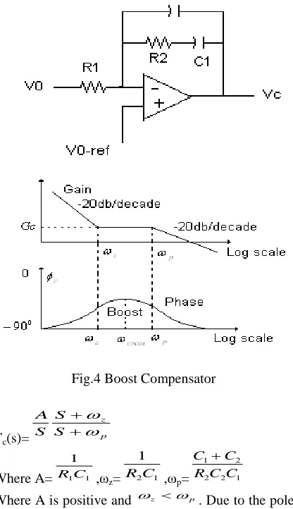
Fig.4 Boost Compensator
Tc(s)= p
z
S S S A
Where A= 1 1 1
C
R ,ω
z= 2 1
1
C
R ,ω
p= 2 2 1
2 1
C C R
C C
Where A is positive and z p. Due to the pole at the origin, the phase of Tc(s) starts with -90º. The
presence of the zero provides a “boost” to be something greater than -90º. Eventually because of the pole at ωp, the phase angle of Tc(s) comes back
down to -90º.
Designing of Boost compensator
The parameters can be designed using K-factor approach. The design procedure of the proposed closed loop boost compensator design for Predictive current mode controller are summarized as below:
Step1: Determine the Crossover frequency ωcross.
The K-factor is used such that
K
cro ss z
cross p K
K can be defined as
2 45
tan boost
K o
Step2: Set the required closed loop PM at the
Crossover frequency, and ,hence, the boost needed from the error amplifier to calculate K in equation. Boost can be defined as
Boost=PM-φ1-90º.
φ1 is the phase angle of the loop transfer function
Ĝv(s) at the crossover frequency. It can be obtained
from the frequency response
Step3: Find the gain Gc(s) of the compensator at
ωcross by using the condition
1
)
(
cross
ol
G
Step4: Set the value for R1From the equations rest
of the parameters can be calculated as fallows:
KR cro ss
G C
11
2
)
1
(
22
1
C
K
C
cro ss
C K R
1
2
IV. SIMULATION RESULTS
The Simulation work is done by using MATLAB/Simulink. The simulation diagram for the PFC Boost rectifier with CMC is shown in Fig.4.1. simulation result of the input current waveform is shown with the component values given by Table I. Form the Fig.4.2 by using the CMC we can get the THD in input current waveform is 6.08%.
Table I
Vg 220V
V0 300
L 25e-3
Fs 5000Hz
K 0.208
C 360e-5
Fig.4 Simulink Boost Compensator For 650 Ohm
Fig. 5 Source current and voltage waveforms of the Boost Rectifier switched by the CMC at R=650Ω For 650 ohms of resistance , source voltage and source currents are as shown in fig. 5 above.
Fig. 6 Output voltage waveforms of the boost rectifier switched by the CMC at R=650Ω For 650 ohms of resistance , output voltage waveforms are as shown in fig .6 above
Fig. 7 Harmonic spectrum of the source current at R=650Ω
For 650 ohms of resistance , Harmonic spectrum is as shown in fig 7 above. and THD is 4.33%.
For 350 Ohm
Fig. 8 Source current and voltage waveforms of the Boost Rectifier switched by the CMC at R=350Ω
For 350 ohms of resistance , source voltage and source currents are as shown in fig. 8 above.
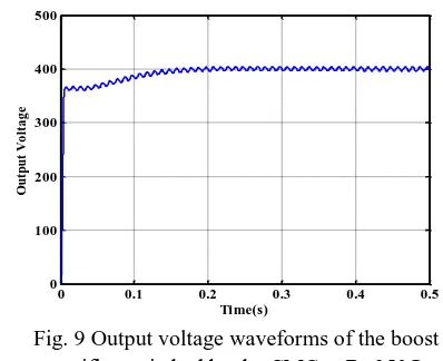
Fig. 9 Output voltage waveforms of the boost rectifier switched by the CMC at R=350Ω For 350 ohms of resistance, output voltage waveforms are as shown in fig.9 above.
Fig. 10 Harmonic spectrum of the source current at R=350Ω
For 350 ohms of resistance , Harmonic spectrum is as shown in fig .10 above. and THD is 2.21%.
V. CONCLUSION
This paper has presented one new and interesting
0.31 0.32 0.33 0.34 0.35 0.36 -10
-5 0 5 10 15
Ti me(s)
So
ur
ce
V
ol
ta
ge
(1
00
V
/D
iv
),
So
ur
ce
C
ur
re
nt
(1
A
/D
iv
)
Source Vol tage Source Current
0 0.1 0.2 0.3 0.4 0.5
0 100 200 300 400 500
Time(s)
O
u
tp
u
t
V
O
lt
a
g
e
0.38 0.39 0.4 0.41 0.42 0.43 0.44 0.45 0.46 -15
-10 -5 0 5 10 15
Time(s)
S
o
u
rc
e
V
o
lt
a
g
e(
1
0
0
V
/D
iv
),
S
o
u
rc
e
C
u
rr
en
t(
1
A
/D
iv
)
Source Voltage Source Current
0 0.1 0.2 0.3 0.4 0.5
0 100 200 300 400 500
Time(s)
O
u
tp
u
t
V
o
lt
a
g
AC/DC boost-type converters for PFC applications. Without using any dedicated converter, one converter can be used to eliminate the harmonic current generated by the other non-linear load. With the help of simulation study, it can be concluded that, this configuration removes almost all lower order harmonics, hence with this configuration we can achieve power factor nearer to unity, THD less than 15%.
REFERENCES
[1]. O.Garcia, LA. Cobos, R. Prieto, P. Alou, J. uceda, “Power Factor Correction: A Survey”, IEEE Trans. Power electron., 2001,pp.8-13.
[2]. Ned. Mohan, Tore M.Undeland, Williams P. Robbins, “Power Electronics Converters, Applications and Design”, John Wiley & Sons (Asia) Pte Ltd. Second Edition, 1995
[3]. Zheren Lai, Keyue Ma Smedly, “A Family of Continuous Conduction-Mode power-Factor-Correction Controllers based on the general pulse-width modulator”, IEEE Trans. On power electronics, Vol.13, no.3, May 1998,pp.501-510
[4]. Robert Mammano “Switching Power Supply topology, Voltage Mode Vs Current Mode”, Unitrode Design note. DN-62.
[5]. Lioyd Dixon “Average Current Mode Control of Switching Power Supplies”Unitrode Design note. DN-140
[6]. J.P.Gegner and C.Q.Lee,’ Linear peak current mode control: A simple active power factor correction control technique for continuous conduction mode”, in Proc. IEEE PESC’96 Conf., 1996, pp.196-202.
[7]. D.Maksimovic, Y.Jang, and R.Erikson, “Non-linear carrier control for high power factor boost rectifiers”, Proc. IEEE APEC’95 Conf., 1995, pp.635-641.
[8]. Souvik Chattopadhayay, V. Ramanarayanan, and V. Jayashankar, “A Predictive Switching Modulator for Current Mode Control of High Power Factor Boost rectifiers”, IEEE Trans. On Power Electronics, vol. 18, No.1, Jan. 2003
[9]. Unitrode Application Note “Modeling, Analysis and Compensation of the Current Programmed Converters”, U-97
[10]. R.D. Middlebook and S.M.C’ui, “A general unified approach to modeling switching converter power stages,” in Proc. IEEE PESC’76 conf., 1976, pp. 18-34.
[11]. F.Dong Tan and R.D. Middlebrook, “A unified Model For Current –Programmed-Converters”, IEEE Trans. Power Electron., Vol. 10, pp.397-408, July 1995.
BIODATA:
Sridhar Konam completed M.tech (power system)