R E S E A R C H
Open Access
A sigma–delta analog to digital converter
based on iterative algorithm
Mohammadmehdi Kafashan
1*, Mahboobeh Ghorbani
2and Farokh Marvasti
1Abstract
In this article, we present a new iterative algorithm aimed at improving the performance of the sigma–delta analog to digital (A/D) converter. We subject the existing sigma–delta modulator, without changing the configuration, to an iterative procedure to increase the signal-to-noise ratio of the reconstructed signal. In other words, we demonstrate that sigma–delta modulated signals can be decoded using the iterative algorithm. Simulation results confirm that the proposed method works very well, even when less complex filters are used. The simple and regular structure of this new A/D converter, not only makes realization of the hardware as ASIC or on FPGA boards easy, but also allows it to operate at high frequency levels with optimized power consumption and small chip area. Implementation of the design with an FPGA shows that experimental results are in agreement with the simulation results.
Introduction
Analog to digital (A/D) convertors are key in many appli-cations of digital signal processing (DSP) and communi-cation systems [1]. Conventional A/D converters consist of two steps: a sampling operation followed by a digi-tal quantization. For uniform sampling, a common clock is operated in order to convert analog signals to digital values [2,3]. In a sigma–delta modulator (SDM), the orig-inal signal is highly oversampled and the internal clock operates at a much higher rate than the bandwidth of the signal; however, the oversampled signal is downsampled at the last stage of the A/D conversion. The noise introduced by signal distortion due to quantization degrades the A/D performance [4-6].
Recovery of the original signal from its distorted version falls into the domain of the inverse problem. Although there are many solutions for this challenge, there isn’t one direct analytic solution [7-9]. In this article, the iter-ative method is used to decrease the distortion caused by modulator. This innovative approach can be imple-mented without any changes to the structure of the SDM by adding a mathematical block after the demodulator of the SDM. Therefore, it can be used easily as a DSP chip for A/D conversion [10].
*Correspondence: [email protected]
1Electrical Engineering Department and Advanced Communications Research Institute (ACRI), Sharif University of Technology, Tehran, Iran
Full list of author information is available at the end of the article
The rest of this article is organized as followed. The next section describes the iterative algorithm for recov-ery of bandlimited signals from their distorted versions. In section “Sigma–delta modulation using the iterative algorithm”, the iterative solution for an A/D conversion is disclosed, followed by analysis and presentation of sim-ulation results. Section “Implementation results of the iterative sigma–delta A/D converter” presents results of the new A/D converter implementation on an FPGA, and finally section “Conclusion” concludes this article.
The iterative algorithm
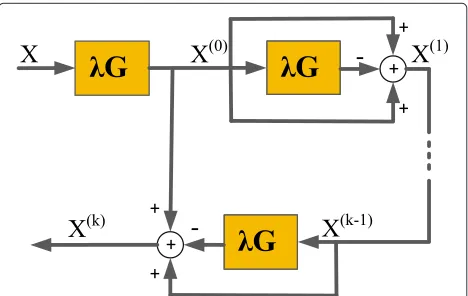
In this section, we first introduce the inverse problem and then explain how the iterative method can be used to solve this problem [11,12]. Consider the system shown in Figure 1, where the input to the system is unknown, but the output and the system (operatorGcalled distortion operator) itself are known. The relation betweeny(t)and x(t)isy(t)=G{x}. The goal is to find the signalx(t)such that it becomes as identical as possible to the input signal x(t).
A simple approach is to use the inverse system of G
which is noted asG−1. Therefore, by feeding the output signaly(t)into the reverse system, the input signal will be reconstructed with no error. However, it is usually diffi-cult to obtain the inverse operator ofG. Hence, we need a technique to approximateG−1based onG. In order to
G
y(t)
x(t)
Figure 1The known system with known output and unknown input signal.
overcome this problem, we unveil our iterative algorithm as follows:
x(k)(t)=x(k−1)(t)+λ(G{x(t)} −G{x(k−1)(t)}) (1)
where x(k)(t) is the kth iteration andG{x(t)}represents the output of the system when no iteration is used. Also,
λdenotes the relaxation parameter, which determines the convergence rate of the algorithm. This means that by using a larger value forλ, fewer iterations are needed to approximate the inverse of the system. In general, G can be either a linear or a non-linear operator. The discrete version of the iterative algorithm, when the distortion operator G is linear, can be written as:
X(k)=GX+(I−G)X(k−1) (2)
where I is an identity matrix of size N × N. X(k) and
G = λGin the above equation are N ×1 and N ×N
matrix, respectively. By defining the operatorE = I−G, the reconstructed signal after k iterations can be written as:
X(k)=(Ek+Ek−1+· · ·+E+I)X(0), X(0)=GX. (3)
The right hand side of the Equation (3) can be simplified using arithmetic progression such that:
X(k)=
I−Ek+1 I−E
X(0) (4)
If the norm of the operator E satisfies E < 1,
by increasing the number of iterations k, Equation (2) approaches the inverse system. Hence,X(k)converges to the original input signalX. The block diagram of the pro-posed iterative method is shown in Figure 2. In order to improve the performance of the approximated inverse system, it is only necessary to increase the number of blocks.
Sigma–delta modulation using the iterative algorithm
Sigma–delta modulator are well established to be used in high resolution A/D conversions [13,14]. The ratio between the sampling rate and twice the signal bandwidth (Nyquist rate) is defined as the oversampling ratio(OSR=
fs/fNyquist). The digital signal is digitally filtered to extract
the analog signal information at high resolution. Typically the filters of the SDM concept are the critical elements and play an important role in determining the resolution of these A/D converters. Therefore, it is necessary to use filters which do not have complex architectures and can be readily utilized to achieve good performance in an A/D converter.
A block diagram of a first order SDM A/D converter is shown in Figure 3. The system consists of an analog SDM followed by a digital decimator. The modulator consists of an integrator, an internal A/D converter or quantizer and a D/A converter (DAC) used in the feedback path. The process of noise shaping by the SDM can be viewed as pushing quantization noise power from the signal band to other frequencies. The modulator output is just a delayed version of the signal plus quantization noise that has been shaped. The modulator output can then be low-pass fil-tered to attenuate the out-of-band quantization noise and finally down-sampled to the Nyquist rate.
Some of the existing techniques to improve the per-formance of SDM A/D converters require increasing the OSR and using higher orders or multi-bits SDMs. The OSR can not exceeded a specific value, and it is limited by the frequency constraint of Sigma–Delta A/D converters,
where fmax is the maximum frequency that can be
sup-ported. Higher order SDMs call for analog circuits which are more advanced and precise than those employed in the 1st order SDM. The main disadvantage of the multi-bit SDMs is that the multi-bit DAC cannot be easily fabri-cated using VLSI technology with adequate linearity. This is essential for high resolution conversion. In addition, the multi-bit output adds to the complexity of the digi-tal low-pass filter (LPF) design that follows the modulator. Since, in multi-bit processing, the filter requires multi-bit hardware multipliers [15,16].
The previous methods have mostly attempted to mod-ify the architecture of SDM A/D converters in order to
Figure 3Architecture of the first order SDM.
0 5 10 15 20 25
-70 -60 -50 -40 -30 -20 -10 0 10
Frequency (MHz)
Magnitude (dB)
Original Sig. SDM output Reconstructed Sig.
Figure 4Spectra of the original signal (a bandlimited gaussian random signal) along with that of the recovered signals with and without using the iterative algorithm (SDM output is the output without iteration, and reconstructed signal is the output signal of the iterative procedure).
0 5 10 15 20
0 10 20 30 40 50 60 70
Iteration Number
SNR(dB)
0 5 10 15 20
0 10 20 30 40 50 60 70
Iteration Number
SNR (dB)
0 5 10 15 20
0 10 20 30 40 50 60 70
Iteration Number
SNR (dB)
0 5 10 15 20
0 10 20 30 40 50 60 70
Iteration number
SNR (dB)
0 5 10 15 20
0 10 20 30 40 50 60 70
Iteration Number
SNR (dB)
0 5 10 15 20
0 10 20 30 40 50 60 70
Iteration number
SNR (dB)
OSR = 16, q = 3 OSR = 32, q = 3 OSR = 64, q = 3
OSR = 16, q = 5 OSR = 32, q = 5 OSR = 64, q = 5
0 5 10 15 20 0
10 20 30 40 50 60 70
Iteration Number
SNR(dB)
0 5 10 15 20
0 10 20 30 40 50 60 70
Iteration Number
SNR (dB)
0 5 10 15 20
0 10 20 30 40 50 60 70
Iteration Number
SNR (dB)
0 5 10 15 20
0 10 20 30 40 50 60 70
Iteration number
SNR (dB)
0 5 10 15 20
0 10 20 30 40 50 60 70
Iteration Number
SNR (dB)
0 5 10 15 20
0 10 20 30 40 50 60 70
Iteration number
SNR (dB)
OSR = 16, q = 3 OSR = 32, q = 3 OSR = 64, q = 3
OSR = 16, q = 5 OSR = 32, q = 5 OSR = 64, q = 5
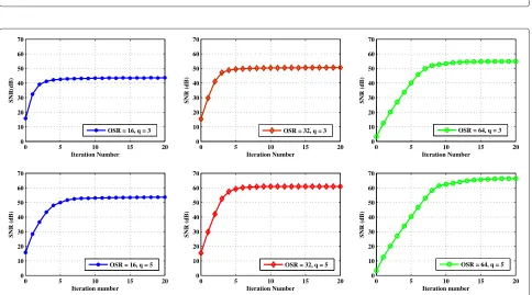
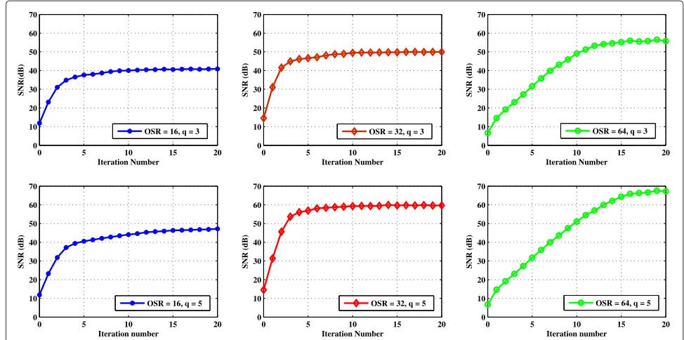
Figure 6SNR of the reconstructed signal versus number of iterations for the first order SDM and IIR filter.
ensure improved A/D converter performance, while the proposed iterative approach exploits a mathematical sig-nal processing algorithm to achieve the same goal. The distortion operatorGfor SDM A/D conversion consists of a SDM and multistage LPF.
Simulations were run for various types of sigma–delta A/D converters for different OSRs, and it is demonstrated in Figures 4 and 5 that the iterative algorithm improves the performance of the first and second order SDM A/D converters. This algorithm can be used for improving the
signal-to-noise ratio (SNR) of the reconstructed signal for all types of SDM A/D.
The spectrum of the original input signal (a bandlim-ited gaussian random signal), the SDM output and the reconstructed signal (using the iterative algorithm after five iterations) are depicted in Figure 4.
It can be seen from Figure 4 that the output of the SDM decreases the noise power in low frequencies which caused an increase in the apparent signal to noise ratio of the resultant signal. Hence, the spectrum of the original
Table 1 SNR of the reconstructed signal versus number of iterations for the second order SDM withλ=1
Iteration number
Filter type OSR Quantization bits 0 2 4 10 15 20
FIR 16 3 18.15 43.58 55.10 57.06 57.19 57.15
5 18.14 43.73 64.18 69.66 69.98 70.02
32 3 15.32 42.0 57.96 60.35 60.58 60.67
5 15.32 42.16 65.08 77.51 78.33 78.48
64 3 21.79 29.63 44.67 67.02 66.46 67.07
5 21.98 29.75 44.42 72.89 78.18 77.90
IIR 16 3 15.40 42.76 49.72 51.04 52.48 52.78
5 15.40 43.66 61.61 63.07 63.40 64.12
32 3 16.12 45.24 57.24 60.16 60.79 61.26
5 17.32 46.34 61.67 66.11 67.15 67.50
64 3 21.65 30.52 38.83 50.03 66.88 76.96
System Model in MATLAB
Extraction of the Hardware Model
Hardware Model in VHDL Hardware Model in MATLAB
Verification of Validity of the Hardware
Figure 7Design flow of the proposed A/D implementation.
signal and output of SDM have the same values at low frequencies. It is also clear that the frequency responses of the original and recovered signals are almost indistin-guishable.
Impressive results have been obtained using the itera-tive algorithm. The SNR of the reconstructed signal versus number of iterations is displayed for the first and sec-ond order SDMs with the two numbers of quantization bits(q = 3, 5). Two types of LPFs have been applied; the first is a simple FIR filter which has 90 taps with Hanning
Table 2 Design summary reported by Xilinx ISE for first order design of the proposed method
Logic utilization Used Available Utilization (%)
Total number slice registers 204 178,176 1
Number used as flip flops 199 N.A. N.A.
Number used as latches 5 N.A. N.A.
Number of four input LUTs 761 178,176 1
Number of occupied slices 459 89,088 1
Number of slices containing only related logic
459 459 100
Number of slices containing unrelated logic
0 459 0
Total number of four input LUTs 764 178,176 1
Number used as logic 761 N.A. N.A
Number used as a route-thru 3 N.A. N.A.
Number of bonded IOBs 143 960 14
IOB flip flops 5 N.A. N.A.
Number of BUFG/BUFGCTRLs 1 32 3
windowing (Figure 5) and the second one is the first type IIR filtering with the order of 9 (Figure 6). Also, three dif-ferent OSRs are examined in our simulations. It can be concluded from the results that by increasing the value of the OSR, the quality of the reconstructed signal improves.
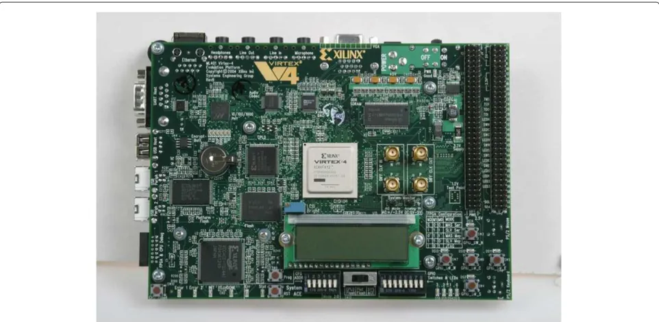
Figure 9Xilinx ML403 evaluation board used for implementation the proposed algorithm.
Simulation results for the second order SDM with FIR and IIR LPFs are shown in Table 1. By comparing the results, we discover that the iterative algorithm enhances the performance of Sigma–Delta A/D converters for dif-ferent types of LPFs and the numbers of quantization bits. Table 1 shows that the highest SNR value is about 60 dB for the second order IIR LPF which is obtained when OSR=64 and quantization bit is 5.
Implementation results of the iterative sigma–delta A/D converter
The sequence began by first implementing the proposed model in VHDL, then performing simulation runs and finally verifying the set up through the Mentor Graphic simulation software, Modelsim 6.0. A 32 bit fixed point number system was used for number presentation in order to better optimize system performance and power consumption. We also used synchronous flip flops as stor-ing elements of the system variables and led feedback from the output of the sigma–delta.
From the original Matlab model of the design, we extracted the hardware model and in the meantime simul-taneously generated an equivalent Matlab model for the hardware model of the design. Finally, after simulations the output of the hardware simulation of the model was compared with that of the Matlab model of the hardware implementation. In this way, we verified the correctness of the hardware model of the design. Figure 7 charts the design flow for this implementation.
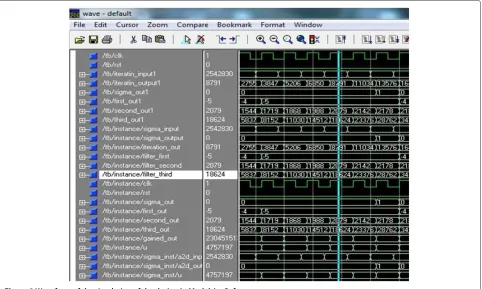
We simulated the design in Modelsim Software using a 5,000 input sample array. Figure 8 shows a snapshot of the
waveform of the simulation. We synthesized the design using Xilinx ISE for the first order SDMs. The device used was Xilinx Virtex4. The SNR values of the reconstructed signal were 23.88, 40.0595 and 40.6420 after one, two and three iterations, respectively. Looking at these figures, it is obvious that only two iterations are enough in order to achieve an increase of 15 dB in the SNR of the output signal. Table 2 shows the synthesize report generated by Xilinx ISE for the first order SDM.
Finally, we implemented the design on a real FPGA board (ML403 evaluation board shown in Figure 9). This required the inclusion of an on-board memory in the FPGA to store 5,000 input samples as an array, with the output of the design communicating to the PC through a Serial Cable and used RS232-UART to communicate with a PC. We then used Microsoft Windows Hyper Terminal Software to prompt get the generated output of the design to check in the Matlab Software.
The design was also evaluated in terms of power con-sumption. We synthesized the design using Synopsys Design Compiler (Version A-2007.12-SP5 for Linux) in
Table 3 Power and area for design reported by synopsys design compiler
Cell Internal Power 153.3550μW (58%)
Net Switching Power 111.8264μW (42%)
Total Dynamic Power 265.1814μW (100%)
Cell Leakage Power 7.3691μW
65 nm technology and measured the power consump-tion by Synopsys Power Compiler Tool. Table 3 shows the power consumption of the iteration in terms of static and dynamic power. For dynamic power consumption, the results are presented for both internal and switching power.
Conclusion
This article presents a new iterative algorithm to convert analog signals to digital signals (A/D) by using a sigma– delta A/D converter. The iterative algorithm has proved itself as an effective tool to remove quantization noise caused by the quantizer and recover the original signal from its distorted version without changing the struc-ture of the existing sigma–delta A/D converters. The main advantage of the proposed algorithm is that it improves the performance of these A/D converters and decreases the distortion caused by the SDM. This latter feature makes the application of lower degree filters possible, which leads to reduced cost and less complexity of the A/D converter design.
The sigma–delta A/D converters can find many prac-tical applications as a result of their simple structures. Implementation of the iterative algorithm is easy, requir-ing no change to the configuration of the A/D converter in order to increase the number of iterations. Another notable advantage of the iterative algorithm is that it sup-ports all types of SDMs with different orders and different numbers of quantization bits.
Competing interests
The authors declare that they have no competing interests.
Author details
1Electrical Engineering Department and Advanced Communications Research
Institute (ACRI), Sharif University of Technology, Tehran, Iran.2Computer Engineering Department, Sharif University of Technology, Tehran, Iran.
Received: 2 September 2011 Accepted: 24 June 2012 Published: 18 July 2012
References
1. R Walden, Analog-to-digital converter survey and analysis. IEEE J. Sel. Areas Commun.17(4), 539–550 (1999)
2. M Unser, Sampling-50 years after Shannon. Proc. IEEE.88(4), 569–587 (2000)
3. J Candy, A Huynh, Double interpolation for digital-to-analog conversion. IEEE Trans. Commun.34, 77–81 (1986)
4. R Schreier, G Temes,Understanding Delta–Sigma Data Converters (Wiley-IEEE Press, New York, 2004)
5. M Kozak, I Kale,Oversampled Delta–Sigma Modulators Analysis, Applications and Novel Topologies(Kluwer Academic, Boston, 2003) 6. M Kafashan, S Beygiharchegani, F Marvasti, Performance improvement of
an optimal family of exponentially accurate sigma delta modulator. in Proc. IEEE International Conference on Signal Processing (ICSP),2010, pp. 1–4 7. F Marvasti,Nonuniform Sampling: Theory and Practice(Kluwer
Academic/plenum, New York, 2001)
8. K Grochenig, Acceleration of the frame algorithm. IEEE Trans. Signal Process.41(12), 3331–3340 (1993)
9. M Kafashan, S Beygi, F Marvasti, Asynchronous analog-to-digital converter based on level-crossing sampling scheme. EURASIP J. Adv. Signal Process.
2011(1), 1–12 (2011)
10. A Oppenheim, R Schafer, J Buck,Discrete-Time Signal Processing. (Prentice Hall, Englewood Cliffs, 1999)
11. F Marvasti, M Analoui, M Gamshadzahi, Recovery of signals from nonuniform samples using iterative methods. IEEE Trans. Signal Process.
39(4), 872–878 (1991)
12. F Marvasti, P Clarkson, M Dokic, U Goenchanart, C Liu, Reconstruction of speech signals with lost samples. IEEE Trans. Signal Process.40(12), 2897–2903 (1992)
13. B Razavi,Principles of Data Conversion System Design(IEEE Press, Piscataway, 1995)
14. F Marvasti, A/D Converters based on sigma delta modulators and iterative methods, United States Patent 7570186, 2009
15. S Norsworthy, R Schreier, G Temes, ICS Society,Delta–Sigma Data Converters: Theory, Design, and Simulation(IEEE Press, Piscataway, 1997) 16. R Gray, Quantization noise spectra. IEEE Trans. Inf. Theory.36(6),
1220–1244 (1990)
doi:10.1186/1687-6180-2012-149
Cite this article as:Kafashanet al.:A sigma–delta analog to digital converter
based on iterative algorithm.EURASIP Journal on Advances in Signal Processing
20122012:149.
Submit your manuscript to a
journal and benefi t from:
7Convenient online submission
7 Rigorous peer review
7Immediate publication on acceptance
7 Open access: articles freely available online
7High visibility within the fi eld
7 Retaining the copyright to your article