Scholarship@Western
Scholarship@Western
Electronic Thesis and Dissertation Repository
4-18-2018 2:30 PM
Development of Nanostructures by Atomic and Molecular Layer
Development of Nanostructures by Atomic and Molecular Layer
Deposition
Deposition
Andrew P. Lushington
The University of Western Ontario Supervisor
Sun, Xueliang
The University of Western Ontario
Graduate Program in Mechanical and Materials Engineering
A thesis submitted in partial fulfillment of the requirements for the degree in Doctor of Philosophy
© Andrew P. Lushington 2018
Follow this and additional works at: https://ir.lib.uwo.ca/etd Part of the Other Materials Science and Engineering Commons
Recommended Citation Recommended Citation
Lushington, Andrew P., "Development of Nanostructures by Atomic and Molecular Layer Deposition" (2018). Electronic Thesis and Dissertation Repository. 5354.
https://ir.lib.uwo.ca/etd/5354
This Dissertation/Thesis is brought to you for free and open access by Scholarship@Western. It has been accepted for inclusion in Electronic Thesis and Dissertation Repository by an authorized administrator of
i
Atomic layer deposition (ALD) is a thin film deposition technique that has a rich history
of being an enabling technique. This vapor phase deposition process can produce a variety of thin
films and nanostructures. ALD is based on sequential, self-limiting reactions and provides
angstrom level control over film growth. Furthermore, ALD allows for conformal deposition on
high-aspect ratio structures and can provide tunable film composition. As nanotechnology marches
forward, the development of nanomaterials has significantly advanced. Additional functionality
can be imparted to nanomaterials by using surface modification techniques. Given the advantages
of ALD, this technique has become a powerful tool for modifying the surface of materials and
increasing the functionality and application of nanomaterials. The toolkit of available materials for
surface modification is further augmented by including molecular layer deposition (MLD), a
technique used to grow organic polymer-like materials. By combining ALD and MLD together,
novel inorganic-organic hybrid materials can be produced with specifically tailored properties.
The first part in the thesis investigates the effect of ozone on nitrogen doped carbon
nanotubes (NCNTs) and pristine carbon nanotubes (PCNTs). The deleterious effects of ozone were
found to occur only for NCNTs, while little to or no damage occurs for PCNTs. Furthermore, this
work highlights the importance of understanding precursor-substrate interaction, especially when
dealing with nanomaterials.
The second and third part of this thesis outline the synthesis of novel thin films made by
ALD and MLD. First, an aluminum alkoxide film with tunable conductivity was made using
trimethylaluminium (TMA), ethylene glycol (EG), and terephthaloyl chloride in various subcycle
configurations to control the ratio of aluminum to carbon in the film. The films were then
pyrolyzed in a reducing atmosphere to yield a conductive aluminum oxide/carbon composite.
Depending on the ratio of aluminum to carbon in the grown film, post-pyrolyzed films displayed
varying levels of electronic conductivity. Synchrotron based XPS was then used to elucidate the
origin of conductivity within the film. The second novel film is a mixed inorganic-organic polyurea
film. For the first time, polarization-dependent x-ray absorption spectroscopy was used to
determine the difference in orientation and ordering between pure organic polyurea films and
inorganic-ii
as electronic conductivity and oligomer packing density.
The fourth part of this thesis investigates the formation of single-atom and ultra-small
clusters of platinum produced by ALD. The self-limiting characteristics of
trimethyl(methylcyclopentadienyl)-platinum on NCNTs and PCNTs was investigated by varying
precursor exposure time and determining the influence of reactor temperature. This study
determined that a 1 minute exposure of the Pt precursor at 250°C yielded primarily single atoms
and ultra-small clusters on NCNTs, but not PCNTs. Extended x-ray fine structure analysis was
conducted to determine the bonding characteristics of Pt to NCNTs and PCNTs. This study
outlines the necessary conditions to deposit single atom and ultra-small clusters of Pt on carbon
nanotube substrates and the parameters that influence this process.
The final experimental investigation of this thesis is the protection of metallic lithium (Li)
by ALD and MLD. Fifty cycles of either TMA-H2O, TMA-EG or TMA-glycerol (GLY) were used
to coat the surface of Li metal. Galvanostatic cycling of Li symmetric cells was then conducted to
determine the protective capabilities of these films. The results revealed that electrodes coated with
TMA-GLY provided prolonged cyclability of metallic Li electrodes. For the first-time gravimetric
intermission titration technique was then conducted on coated electrodes to unravel the effects of
lithium electrodissolution and electroplating. This study demonstrated that the longevity of
TMA-GLY coated electrodes originates from the relatively low overpotential required to plate and strip
Li from the MLD film. Finally, scanning electron microscopy and Rutherford backscattering
spectometry was used to determine composition and morphology of the formed solid electrolyte
interphase on coated electrodes following electrochemical cycling.
Keywords
iii
1.
Title: Surface Modification of Nitrogen Doped Carbon Nanotubes by Ozone via Atomic Layer Deposition
Authors: Andrew Lushington, Jian Liu, Yongji Tang, Ruying Li, and Xueliang Sun
The final version of this manuscript has been published in the Journal of Vacuum Science & Technology A, 2014, 32, 01A124. Jian Liu helped with ALD experiments and production of nitrogen doped carbon nanotubes. Yongji Tang conducted Raman spectroscopy measurements. Ruying Li provided access to all equipment. All authors contributed editorial comments on the manuscript.
2.
Title: A Novel Approach in Controlling the Conductivity of Thin Films Using Molecular Layer Deposition
Authors: Andrew Lushington, Jian Liu, Mohammad N. Banis, Biwei Xiao, Stephen Lawes, Ruying Li, Xueliang Sun.
The final version of this manuscript has been published in Applied Surface Science, 2015, 357, 1319. Jian Liu provided assistance with manuscript writing, figure design and ALD/MLD experiment design. Mohammad N. Banis conducted synchrotron based X-ray tests. Biwei Xiao conducted Raman spectroscopy measurements. Stephen Lawes aided in construction of four-point probe and analysis of conductivity measurements. Ruying Li provided access to the equipment. All authors contributed editorial comments on the manuscript.
3.
Title: Orientation and Ordering of Organic and Hybrid Inorganic-Organic Polyurea Films Using Molecular Layer Deposition
Authors: Andrew Lushington, Craig Langford, Jian Liu, Kaiqi Nie, Ruying Li, Xuhui Sun, Jinghua Guo, and Xueliang Sun.
iv
Regulated Gas Phase Chemisorption.
Authors: Andrew Lushington, Samantha Stambula, Mohammad N. Banis, Niancai Cheng, Yang Zhou, Ruying Li, Tsun-Kong Sham, Gianluigi A. Botton, and Xueliang Sun
This manuscript is currently in preparation for submission. Both Andrew Lushington and Samantha Stambula contributed equally to this work. Samantha conducted TEM analysis and data acquisition. Mohammad N. Banis performed synchrotron experiments at CLS. Niancai Cheng helped with experimental design. Yang Zhou conducted ICP experiments and provided analysis of ICP data. Ruying Li provided access to all equipment. Tsun-Kong sham helped with analysis of synchrotron data. All authors contributed editorial comments on the manuscript
5.
Title: Deconvoluting the Effects of Stripping and Plating of Lithium Coated using ALD and MLD.
Authors: Andrew Lushington, Yang Zhao, Lyudmila V. Goncharova, Qian Sun, Ruying Li, and Xueliang Sun.
vi
This Ph.D. work was carried on in Professor Andy Xueliang Sun’s Nanomaterials and
Energy Group at the University of Western Ontario (UWO). Here, it is with my pleasure that I
acknowledge every individual who has accompanied with me and contributed to my work in the
past five years.
I would like to give my sincerest gratitude to Professor Xueliang Sun. He has provided me
with an incredible platform to launch my professional carrier from. His dedication, guidance,
passion, kind-hearted nature, and genuine scientific curiosity will forever serve as a guiding star
for me. Never have I witnessed such a delicate balance between ambition, time management, and
earnestness. His character will always stand as a central pillar in my life and I am truly grateful to
have been under his guidance these past 5 years.
I would also like to personally thank Mrs. Ruying (Kathy) Li. Her kind hearted and loving
nature are really sold short by such simple adjectives. In the past 5 years she has demonstrated
what it means to show unconditional love to all attributes of life. Whether it be a scientific inquiry
or facing a tough life decision, Kathy is always there to listen and provide the sincerest of
responses. Thank you so much for your help over the years, your gratitude and sincerity will not
be forgotten.
I am grateful to Prof. Jian Liu for providing me with an excellent introduction into Prof.
Sun’s group. I will never forget how enthusiastic we would get talking about ALD and the long
days spent fixing vacuum pumps and cleaning oil. I would also like to thank all past and current
group members. There are many times where I felt very proud to be part of such an ambitious
group of researchers. Especially, I would like to thank Dr. Qian Sun, Dr. Xifei Li, Dr. Hossein
Yadegari, Dr. Niancai Cheng, and Dr. Mohammad N. Banis. These individuals were an invaluable
source of information and our interactions will always be remembered. The amount of information
I have learned from these individuals is irreplaceable. I will especially like to mention Dr. Biqiong
Wang, Dr. Biwei Xiao, Dr. Xia Li. We all started this academic journey around the same time and
watching each of our careers expand has been nothing short of fascinating. I am very grateful to
have shared this experience with you guys and I hope our paths cross again in the future. I would
vii
I am grateful to Dr. Tsun-Kong Sham in the Department of Chemistry at Western
University and Dr. Jinghua Guo at the Advanced Light Source at Lawrence Berkeley National
Laboratory, for their help on synchrotron based X-ray studies and analysis. Both of you provided
an excellent platform for me to quench my thirst for fundamental knowledge.
I am also grateful to my advisory committee members, Prof. Robert Klassen and Prof Jun
Yang for their advice, support, and concern during my PhD.
I would like to thank Mr. Stephen Lawes, Mr. Craig Langford, Ms. Mudi Kadu, Mr. Adam
Riese, Ms. Anastasia Pasche, Mr. Benjamin Steen, Mr. Zachary Linder, and Mr. Spencer Yim. I
am incredible luckily that our paths crossed here in London, ON. I learned so much of what
friendship means from you guys and I will forever be grateful for that. I can’t even imagine what
this journey would look like without your support and quirky natures. From late night chess games
to unforgettable nights at BETA and CODA, your friendship will always be remembered.
I would also like to give the sincerest thanks to the Ottawa/Toronto crew, Mr. Alec (the
fetus) Murphy, Ms. Kaitlyn Young, Mr. Vlad Tohaneau, Ms. Indra Calu, Ms. Aretha Heenan and
Mr. Jeremy St. Onge. Without you guys in Toronto I don’t know what I would have done. The
countless nights of escape and mental support you guys provided will never be forgotten. You
guys were an invaluable part of this journey and I give you all the thanks and love. To Mr.
Christopher Demelo, Mr. Phil Zelkie, Mr. Ryan Riddle and Mrs. Monica Nuyens, thank you for
filling in the nerdy hole in my heart with your SnargeCo brand products. I am also grateful to the
whole Easby family for providing such a warm and loving home. Your family dynamic will never
be forgotten and will forever serve as a reminder to what a loving family really means.
I would also like to give my sincerest thanks to the members of MF DOOM. You are an
incredible group people who I am truly glad to call friends. Your support and friendship during
those especially difficult times will be cherished. You guys have shown me that regardless of
geographic location, true friendships can still be forged, especially in the salt mines of the crucible.
You guys have really been a crucial aspect of this process and for that I am truly grateful. Thank
viii
you both mean to me. Your encouragement, motivation, and support over the past few years are
incalculable. You guys are the source of my happiness and motivation and have taught me to
successfully walk a fine line between confidence and doubt. I would also like my thank my brother
and sister-in law, Joy and Jolene Lushington. The love and admiration you both demonstrate to
each other is simply amazing. There is no doubt in my mind that Aliyah will growth up to be as
kind hearted, honest, and loving as your two are.
Thank you all for your love and support. There is no way I could have gotten to where I
am without you all of you.
Andrew Lushington
ix
Co-Authorship Statement... iii
Acknowledgments... vi
Table of Contents ... ix
List of Tables ... xiii
List of Figures ... xiv
List of Appendices ... xx
List of Abbreviations ... xxi
Chapter 1 - Introduction and Literature Review………..………..1
1.1 Introduction to this Thesis ... 1
1.1.1 Energy Storage and Conversion ... 1
1.1.2 Atomic and Molecular Layer Deposition ... 2
1.2 Thesis Objectives ... 3
1.3 Thesis Organization ... 4
1.4 Introduction to Fundamentals ... 6
1.4.1 Gas Phase Deposition Techniques ... 6
1.4.2 Physical Vapor Deposition ... 7
1.4.3 Chemical Vapor Deposition ... 8
1.4.4 Atomic Layer Deposition ... 12
1.4.5 Molecular Layer Deposition ... 17
1.5 Literature Review... 20
1.5.1 Unique Capabilities of ALD ... 20
1.5.2 Unique Capabilities of MLD ... 24
1.5.3 Use of ALD and MLD for Lithium-based Batteries ... 26
1.5.4 ALD and MLD for Lithium-ion Batteries ... 27
1.5.5 ALD and MLD for Lithium-Sulfur Batteries ... 31
1.5.6 Application of ALD and MLD for Fuel Cells ... 33
x
2.1 Experimental Apparatus... 45
2.1.1 Savannah 100 (Cambridge Nanotech, USA) ... 45
2.1.2 Gemstar-8 (Arradiance, USA) ... 48
2.2 Characterization Techniques ... 50
2.2.1 Scanning Electron Microscopy ... 50
2.2.2 Fourier Transform Infrared Spectroscopy ... 52
2.2.3 Raman Spectroscopy ... 54
2.2.4 Quartz Crystal Microbalance ... 55
2.2.5 X-ray Reflectivity ... 57
2.2.6 Synchrotron Based Characterization Techniques ... 58
2.2.6.1 Near Edge X-ray Absorption Fine Structure Spectroscopy ... 59
2.2.6.2 Extended X-ray Absorption Fine Structure Spectroscopy ... 60
2.3 References ... 63
Chapter 3 - Surface Modification of Nitrogen Doped Carbon Nanotubes by Ozone via Atomic Layer Deposition…..………...…………..…....…..64
3.1 Introduction ... 65
3.2 Experimental Details ... 67
3.3 Results and Discussion ... 68
3.4 Conclusions ... 78
3.5 Supporting Information ... 79
3.6 References ... 81
Chapter 4 - Controlling the Conductivity of Thin Films using Molecular Layer Deposition...85
4.1 Introduction ... 86
4.2 Experimental Details ... 87
4.3 Results and Discussion ... 88
4.4 Conclusions ... 95
xi
5.1 Introduction ... 101
5.2 Experimental Details ... 103
5.3 Results and Discussion ... 104
5.4 Conclusions ... 114
5.5 References ... 115
Chapter 6 - Single-Atom and Clusters to Nanoparticles: Controlling the Nucleation of Pt Through Regulated Gas Phase Chemisorption ...119
6.1 Introduction ... 120
6.2 Experimental Details ... 122
6.3 Results and Discussion ... 124
6.4 Conclusion ... 133
6.5 Supporting Information ... 135
6.5.1 Data Processing ... 135
6.5.2 Elemental Quantification ... 140
6.5.3 Additional Histograms ... 142
6.6 References. ... 143
Chapter 7 - Deconvoluting the Effects of Stripping and Plating of Lithium Coated using ALD and MLD ...147
7.1 Introduction ... 148
7.2 Experimental ... 151
7.3 Results and Discussion ... 152
7.3.1 Galvanostatic cycling of Li-Li symmetric cells ... 152
7.3.2 Galvanostatic Intermission Titration Technique ... 156
7.3.3 Morphology Analysis by Scanning Electron Microscopy ... 161
7.3.4 Rutherford Backscattering Spectroscopy ... 163
7.4 Conclusions ... 164
7.5 Supporting Information ... 166
xii
8.2 Thesis Novelties…….….………..178
8.3 Future Perspective ... 179
Appendices ... 183
Appendix A: Permission from AIP for Published Article ... 183
Appendix B: Permission from Elsevier for Published Article ... 184
Appendix C: Permission from ACS for Published Article ... 185
xiii
Table 1.1. Overview of various ALD coatings applied to different Li-ion battery cathode materials……….……28
Table 3.1. XPS survey analysis comparison between untreated NCNTs and 300°C ozone treated NCNTs………...…75
Table 6.1. Comparison of density and diameter data obtained from HAADF-STEM for NCNTs and PCNTs exposed to MeCpPtMe3 at different temperatures and dosing times. ICP analysis was
performed to determine the atomic weight percent of Pt on each sample analyzed in HAADF-STEM………...…128
Table S6.1 Number of images analyzed, and the number of Pt entities counted per image……...139
xiv
Figure 1.1. Family tree diagram of common thin film deposition techniques [4]. Processes central to this thesis are highlighted in red………7
Figure 1.2. Schematic diagram demonstrating film deposition using PVD on a structured substrate………...8
Figure 1.3. Schematic diagram demonstrating film deposition using CVD on a structured substrate………...9
Figure 1.4. Schematic diagram demonstrating film deposition using CVD on a structured substrate………..………...10
Figure 1.5. Arrhenius plot outlining the influence of temperature on growth rate of CVD films [17]……….………....12
Figure 1.6. a) Flow process of ALD cycle consisting of two half steps with alternating cycles of precursor and reactant dosing separated by a purge step. b) Practical growth conditions for ALD of particles and thin films. c) Saturating pulse conditions to achieve self-limiting growth…...…13
Figure 1.7. Temperature dependence for the growth of ALD films………..………..14
Figure 1.8. Demonstration of substrate effect on growth rate……….…………15
Figure 1.9. Schematic diagram demonstrating film deposition using ALD on a structured substrate……….16
Figure 1.10. Table summarizing materials grown by ALD [21]……….……16
Figure 1.11. Schematic of MLD using bifunctional monomers with “triangular” or “square” functional groups [23]………18
Figure 1.12. Ideally, organic precursor molecules should react with only one surface site with film growth occurring vertically. However, molecules may react twice and polymer chain may have tilt perpendicular to the surface [32]………19
Figure 1.13. Borosilicate glass microcapillary array functionalized using ALD. Film resistance can be tailored to suit the application. Materials with high stable secondary emission properties can be used since they are decoupled from the substrate [45]………..….22
Figure 1.14. Diagram demonstrating the various opportunities that ALD provides for the deposition of nanoparticles. ALD can be used to control (1) the size of particles, and (2), (3), (4) particle composition. The highly uniform nature of ALD can be used to deposit particles over A) high aspect ratio trenches and holes, B) on powders and microspheres and C) on nanostructures substrates such as nanowires [52]………...23
xv
Figure 1.17. Various interfacial reactions that can occur at the electrode/electrolyte interface that can be detrimental to battery performance [70]………..………..………..27
Figure 1.18. Schematic for the controlled layer chemistry of aluminum glycerol (AlGL) films used to coat Si nanocomposite electrodes [87]……….………...30
Figure 1.19. a), c) TEM micrograph and b) HAADF-STEM of nano-Si coated with aluminum organic thin film. d) EELS elemental mapping of aluminum organic thin film. e) comparison of cycling capacity of coated and un coated nano silicon and f) rate test of coated nano silicon [88]………...………..31
Figure 1.20. MLD alucone coating for safe high temperature Li-S batteries in carbonate based electrolytes [101] ……….…...33
Figure 1.21. Schematic diagram of platinum encapsulated in zirconia nanocages produced using area-selective ALD [108] ……….……….35
Figure 2.1. Outline of various components of an ALD S100 Cambridge Savannah tool starting with precursor distribution manifold assembly followed by reactor and exhaust assembly…...46
Figure 2.2. a) Birds eye view of the Gemstar-8 system with labels. b) and c) Interior of ALD reaction chamber demonstrating precursor inlet, outlet, and pressure sensor location. d) Inert gas vapor pressure assist line attached to the organometallic manifold………...………....49
Figure 2.3.a) Schematic drawing of a conventional SEM. b) Outline of electron beam interaction with sample and the various signals that can be produced by this interaction [1]………....51
Figure 2.4. a) Schematic outline for the working principle of FTIR. b) Photo of the Thermo Scientific Nicolet 380 FTIR system used………53
Figure 2.5.a) Schematic outline of various types of light scatter that can occur following sample irradiation with a laser source [4]. b) Photo of the HORIBA Scientific LabRAM HR Raman spectrometer used………...…55
Figure 2.6.a) Schematic outline of Phoenix QCM crystal head assay provided by Colnatec [7]. b) Use of QCM in Gemstar-8 ALD system………..………...57
Figure 2.7. a) Schematic outline of operational setup to perform XRR. b) Typical XRR curve outlining the importance of curve features. c) Photo of the Bruker D8 Advance used for XRR….58
Figure 2.8.a) Schematic outline of core-hole excitation by X-rays to higher energy levels and b) generation of Auger electrons via Auger decay to fill empty core-hole states [11]. Measurements of X-ray absorption by c) transmission based techniques and d) electron yield techniques. E) depiction of TEY cascade effect caused by Auger electron emission [12]……….….60
xvi
Figure 3.3. TEM images a) untreated NCNTs, ozone treated NCNTs at b) 150°C, c) 250°C for 500 cycles……….…….71
Figure 3.4. Raman spectra of a) NCNTs and before and after ozone treatment at different temperatures; b) Comparison of ID/IG ratio for NCNTs at different temperatures, ALD cycles, and
ozone pulse time………...72
Figure 3.5. HRTEM image a) untreated NCNTs, and ozone treated NCNTs at b) 150°C, c), d) 250°C. Scale bar in white represents 10 nm………73
Figure 3.6. a) N2 adsorption-desorption isotherms at 77K and b) pore size distribution of as
produced NCNTs and 300°C ozone treated carbon NCNTs……….….74
Figure 3.7. N 1s spectra for NCNTs a) before ozone treatment and b) after ozone treatment at 300°C for 500 cycles……….……….………....76
Figure S3.1. XPS survey spectrum a) before ozone treatment and b) after 300°C ozone treatment………79
Figure S3.2. High resolution XPS of C 1s spectrum a) before ozone treatment and b) after 300°C ozone treatment………..79
Figure S3.3. Raman spectra of a) PCNTs and before and after ozone treatment at different temperatures; b) Comparison of ID/IG ratio for PCNTs at different temperatures, ALD cycles, and
ozone pulse time……….80
Figure 4.1. Mechanism of MLD reaction between TMA, EG and TC………89
Figure 4.2. SEM cross section view of MLD films deposited using a sequence of 1:1 with increasing cycling number. Scale bar represents 50 nm………..89
Figure 4.3. Thickness of 1:1, 1:3 and TMA-EG MLD films verses number of deposition cycles at 150°C……….…90
Figure 4.4. FTIR spectra for 100nm thick TMA-EG, 1:1 and 1:3 MLD films deposited on double polished Si at 150°C………..…….91
Figure 4.5. Raman spectra for a) 1:1 and b) 1:3 MLD films with initial thickness of 200nm annealed with 5% H2/Ar at 600, 700, 800 and 900°C for 1 hour………...…..92
Figure 4.6. Sheet resistance measurements for 100nm thick TMA-EG, 1:1, and 1:3 MLD films pyrolyzed at various temperatures………..………94
Figure 4.7. Synchrotron based XPS of a) as deposited and b) 800°C pyrolyzed TMA-EG and 1:3 MLD films………..95
xvii
TMA……….106
Figure 5.2. FTIR spectra of PDIC-ED (black) and TMA-ED-PDIC (red) films grown on double polished Si. Characteristic polyurea bonds are outlined………...…107
Figure 5.3. a) C 1s and b) N1s NEXAFS spectra of 25 nm TMA-ED-PDIC and PDIC-ED polymers grown at 50°C acquired using total electron yield………...……….108
Figure 5.4. Polarization dependent NEXAFS data taken at for a) PDIC-ED b) TMA-ED-PDIC..110
Figure 5.5. Interpretation of NEXAFS orientation signatures for disordered films. (a) Polarization dependence of the π* bond with fits using the model with fixed tilt angle. Using a model assuming that π* orbitals have random azimuthal orientation and Gaussian distribution of tilt angles with an average tilt τ. The width of this distribution, serves as an orientation disorder parameter. The smaller δ is the more ordered the system is. (b) Solutions to τ and δ using Aπ values for
TMA-ED-PDIC and ED-TMA-ED-PDIC. (c) Schematic diagram outlining the significance of τ and δ values…...….112
Figure 5.6. Depiction of structural morphology of (a) hybrid inorganic-organic polyurea films and (b) pure organic polyurea films……….……113
Figure 6.1. HAADF-STEM images of ALD Pt deposition on NCNTs at 250°C using a dosing time of (a) 1 minute, (b) 30 minutes, and (c) 60 minutes. Experimental (d) PSD histograms were acquired from six different NCNTs for each sample. Image quantification steps and raw/processed images can be found in the supporting information………..…126
Figure 6.2. PSD comparison for (a) a 1 minute exposure of Pt to NCNTs at a temperature of 100°C, 175°C, and 250°C, and (b) a 30 minute exposure of Pt to NCNTs at a temperature of 100°C and 250°C………...128
Figure 6.3. HAADF-STEM images of single pulsed Pt deposited at 250°C on a (a) NCNT and (b) PCNT for a 1 minute exposure. PSD comparison of (c) a 1 minute exposure on NCNTs and PCNTs and (d) a 1 minute and 30 minute exposure on PCNTs………..129
Scheme 6.1. Representation of the chemisorption of MeCpPtMe3 species on defective graphene
and graphene oxide………...……130
Figure 6.4. (a) Pt L3-edge XANES of samples prepared using varying dosing times of MeCpPtMe3
on NCNTs and PCNTs at 250°C along with standard Pt and PtO2. (b) Pt L3 edge k2-weighted
xviii
(b) background from (a), thus forming the (c) background subtracted image. Pt was then (d) manually removed using the polygon selection tool in ImageJ. Digital Micrograph software was used to subtract image (d) from (a) to produce image (e), wherein the (f) threshold was adjusted, and the image was (g) analyzed with ImageJ………..…..136
Figure S6.2 Error analysis for the Pt quantification process. Histogram showing the (a) total counts for the Pt entities as a function of the number of pixels, summed from a five day data analysis of a single image. (b) Fitted Gaussian model and parameters from the low range peak in (a)………..138
Figure S6.3 Error analysis results from a five day study of a single HAADF image with bins showing the experimental error. Data analysis from a single image showing (a) each individual analysis over five days and (b) the mean and standard deviation for each bin from the five day measurement. The errors in (b) represent the error introduced into the measurement from the manual process………...138
Figure S6.4 High energy EELS analysis of Pt deposited on NCNTs for 60 minutes at a temperature of 250°C was imaged using ADF (a) before and (b) after the EELS acquisition. The (c) ADF image corresponding to the (d) spectrum image shows that the bright spots correlate to a Pt-L edge, as shown in the (e) extracted spectra from the areas outlined in (c) and (d)………...142
Figure S6.5. PSD histograms from (a) NCNTs at 100°C using a dosing time of 1 minute, and 30 minutes, and (b) NCNTs and PCNTs at 250°C using a dosing time 30 minutes………....142
Figure 7.1. Galvanostatic cycling of Li-Li symmetric cells at a current density of 1 mA cm-2 until
a capacity of 1 mAh cm-2 is reached. Cells are cycled in EC/DEC/DMC electrolyte with 1M
LiPF6………153
Figure 7.2. Galvanostatic cycling of Li-Li symmetric cells at a current density of 3 mA cm-2 until a capacity of 2 mAh cm-2 is reached. Cells are cycled in EC/DEC/DMC electrolyte with 1M
LiPF6………155
Figure 7.3. a) First few cycles of GITT data for bare Li outlining an envelope voltage pattern. b) Cells are cycled using a 15s current pulse at a density of 5 mA cm-2 followed by a rest period of 3
minutes until a capacity of 5 mAh cm-2 is attained. c) 10 GITT cycles for bare Li cell………….158
Figure 7.4. GITT experiments for half-cell configurations of TMA-GLY or TMA-H2O as either anode and cathode against bare Li. Schematic outline for configuration employed can be found at the top right corner of each graph……….……159
Figure 7.5. Cross section SEM images of lithium surface following 1st half cycle (0-a) using GITT (top row) and top view SEM images of the same electrodes after 5 galvanostatic cycles. Scale bar in white represents 100 μm………...……161
Figure 7.6. RBS spectra and calculated depth profile for bare Li (a, d), TMA-H2O coated Li (b, e), and TMA-GLY coated Li (c, f) following 60 cycles of plating and stripping at 3 mA cm-2 using
a capacity of 2 mAh cm-2………..163
Figure S7.1. Galvanostatic cycling of Li-Li symmetric cells at a current density of 3mA cm-2 until
xix
Figure S7.3. GITT experiments for half-cell configurations of TMA-GLY anode and cathode against bare Li. Schematic outline for configuration employed can be found at the top right corner of each graph………165
xx
Appendix A: Permission from AIP for Published Article………..……...179
Appendix B: Permission from Elsevier for Published Article………..180
xxi
AEY Auger electron yield
ALD Atomic layer deposition
BET Brunauer-Emmett-Teller
BJH Barrett-Joyner-Halenda
BN Boron nitride
CFM Cubic feet per minute
CLS Canadian light source
CNTs Carbon nanotubes
CVD Chemical vapor deposition
DEC Diethyl carbonate
DMC Dimethyl carbonate
EC Ethylene carbonate
ED Ethylenediamine
EELS Energy electron loss spectroscopy
EFSTEM Energy filtered scanning tunneling electron microscopy
EG Ethylene glycol
EHMO Extended Huckle molecular orbital
EMC Ethyl methyl carbonate
EXAFS Extended X-ray absorption fine structure
xxii
GLY Glycerol
GPC Growth per cycle
HAADF High angle annular dark field scanning
HER Hydrogen evolution reaction
HOPG Highly oriented pyrolytic graphite
HOR Hydrogen oxidation reaction
HRTEM High resolution transmission microscopy
ICP-AES Inductively coupled plasma optical emission spectroscopy
IR Infrared
LIB Lithium-ion battery
Li-S Lithium sulfur battery
MCP Microchannel plate
MeCpPtMe3 trimethyl(methylcyclopentadienyl)-platinum (IV)
MFC Mass flow controller
MLD Molecular layer deposition
MOCVD Metal-organic chemical vapor deposition
NCNT Nitrogen doped carbon nanotube
NEXAFS Near-edge X-ray absorption find structure
NP Nanoparticle
OER Oxygen evolution reaction
xxiii
PDIC 1,4 phenylene diisocyonate
PSD Particle size distribution
PVD Physical vapor deposition
QCM Quartz crystal microbalance
RBS Rutherford backscattering spectroscopy
ROI Region of interest
RT Room temperature
S100 Savannah 100 ALD system
SEI Solid electrolyte interphase
SEM Scanning electron microscope
STEM Scanning transmission electron microscopy
TC Terephthaloyl chloride
TEM Transmission electron microscopy
TEY Total electron yield
TFEL Thin film electroluminescent
TMA Trimethylaluminum
VLS-PGM Variable line spacing plane grating monochromator
XAFS X-ray absorption fine structure
XANES X-ray absorption near edge spectroscopy
XPS X-ray photoelectron spectroscopy
1
Introduction and Literature Review
1.1
Introduction to This Thesis
1.1.1
Energy Storage and Conversion
It is often said that necessity is the mother of innovation. This statement holds true for
global warming, As it becomes an increasingly pertinent issue certain technological fields have
experienced rapid advancement. and this certainly is the case for global warming. One avenue
toward curbing the progression of global warming, is shifting away from the use of fossil fuels.
Unfortunately, 85% of the worlds energy use is currently derived from fossil fuel sources [1]. This
rate of consumption is not sustainable and maintaining our present course will lead to irreversible
and unanticipated consequences to our complex climate system. Although fossil fuels will continue
remain a significant source of energy in the next few decades, a path toward a more sustainable
means of energy production use can be envisioned. This path would involve transitioning to clean
and renewable energy sources such as solar and wind. Transmission and distribution of electricity
would also need to be accurately controlled to allow for efficient use of energy. Additionally,
major disruptions within the chemical industry need to occur so that CO2 and H2O can be
economically converted to produce fuels and chemicals to serve our desired needs rather than
relying on oil and gas feedstocks.
For this path to be attainable, significant advancements in the field of energy storage and
conversion are required. Electricity produced from intermittent sources, such as solar and wind,
need to be stored in energy storage devices so that it may be distributed and transmitted efficiently.
Numerous energy storage systems are currently available such as pumped hydro storage, flywheel
energy storage, and compressed air energy storage [2]. However, electrochemical energy storage
systems are uniquely positioned to address future energy storage needs. Lithium-based batteries
Furthermore, as we move toward a more design-oriented world, a need for energy storage devices
with high volumetric energy density is required. Lithium-based batteries, especially all-solid-state
batteries, can address this need. These distinct characteristic makes them ideal for use in electric
vehicles. Electrification of the transportation sector would result in significant reduction in the
production of environmental pollutants caused combustion of fossil fuels.
Currently the successful use of hydrogen as a fuel source is a scientific and technological
challenge and remains elusive. However, if addressed appropriately this technological
achievement would significantly change our use of fossil fuels and provide an opportunity toward
achieving energy sustainability. One method toward achieving a sustainable hydrogen economy is
accurate control over the water splitting reaction, 2H2O 2H2 + O2. This reaction can be broken
down into four half reactions: hydrogen evolution reaction (HER), oxygen evolution reaction
(OER), hydrogen oxidation reaction (HOR), and oxygen reduction reaction (ORR). Both the HOR
and ORR reaction can be utilized in fuel cell devices that convert hydrogen or some other fuel
source into water while the HER and OER reaction are used for hydrogen fuel production. For
these reactions to occur in the economically efficient manner the use of precious metal catalysts
are required. Developing effective catalysts that can easily facility bond-making and bond breaking
reaction at the electrode-electrolyte interface remains a key priority for materials scientists
working in this field [3].
For this envisioned sustainable energy economy to be successful, several scientific and
technological challenges first need be addressed. Many of these challenges are materials related
and require innovative solutions by materials scientists.
1.1.2
Atomic and Molecular Layer Deposition
Atomic layer deposition (ALD) is a vapor phase technique used to deposit thin films and
nanostructures. It is a technique that has pushed the advancement of semiconductor technology
and hold promise for application in the field of energy storage and conversion. As materials
become increasingly complex and move toward the nanoscale regime, coating techniques that can
provide accurate control of growth and material composition becoming increasingly necessary.
ALD can provide both these advantages due to its cyclic, self-saturating nature. This advantage
results in ALD being the technique of choice for coating nanomaterials compared to other
the ALD process consists of introducing gaseous chemical precursors that can react to the
substrate. Additionally, a purge step separates precursor introduction ensuring that gas-surface
reactions occur as half-reactions. This allows for each dose of the precursor to completely react
with the substrate through a self-limiting process. As a result, ALD is a non-line-of-sight technique
that can conformally coat complex, nanostructure substrates in a pin-hole free manner. Although
ALD can be used to grow thin films, careful selection of substrate and chemical precursor can
allow for the growth of nanoparticles. This imparts ALD with the ability to grow particles with
angstrom level control. Furthermore, particles can be grown in a non-line-of-sight fashion on
nanomaterials, providing an optimal route in taking advantage of high surface area to volume
materials.
While ALD is typically used to grow inorganic materials, molecular layer deposition
(MLD) can be used to grow organic polymeric materials. MLD is based on the same fundamental
principles as ALD and involves the use of self-limiting surface reactions. However, MLD
introduces a molecular fragment being deposited during each ALD cycle rather than an inorganic
one that is either oxidized or reduced. Furthermore, ALD and MLD can be combined to create
hybrid inorganic-organic materials and provides many exciting opportunities for materials
scientists. By combining the properties of inorganic materials with that of organic ones, unique
coating materials and nanostructures can be produced by ALD and MLD with tunable properties.
Furthermore, nanolaminate materials can be produced with these two techniques to create novel
properties.
ALD and MLD are two powerful techniques that can be used to address challenges faced
by materials scientists. These techniques provide an avenue toward engineering material properties
and allow scientists to expand the capabilities of currently available materials.
1.2
Thesis Objectives
This thesis focuses on understanding material surface properties and developing novel thin
films and nanostructures. This understanding is then applied to enhance materials with potential
use in lithium-based batteries and fuel cells. The main research objects are listed below:
1. To understand the influence of ozone based ALD techniques on carbon nanotubes and
nitrogen doped carbon nanotubes.
2. Development of thin films with tunable conductivity by combining the techniques of ALD
and MLD.
3. To develop a polyurea based films by ALD and MLD that have a high degree of hydrogen
bonding. Further, understanding the influence of these techniques on polymer properties such
as orientation and packing order is explored. Synchrotron based radiation is used to determine
film properties.
Part 2. Application of ALD and MLD to energy storage and conversion
1. To understand the deposition characteristics of Pt on nanomaterial substrates. Different
deposition parameters are explored in order to try and develop a process that can accurately
control the growth of Pt from single atoms to clusters.
2. Apply techniques of ALD and MLD to metallic lithium electrodes. To control reactions at the
electrolyte/electrode interface, various ALD and MLD coatings with different properties are
applied to Li foil. The effects of lithium electroplating and electrodissolution on these coatings
are explored and discussed.
1.3
Thesis Organization
This thesis consists of eight chapters, an introductory chapter, an experimental chapter, five
articles and one conclusion chapter. It is organized according to the requirements outlined by the
Thesis Regulation Guide provided by the School of Graduate and Postdoctoral Studies at the
University of Western Ontario in the form of an “integrated-article”. The following parts are
included
Chapter 1 introduces various gas phase deposition techniques to provide background fundamental
knowledge. This platform is then used to describe the techniques of atomic layer deposition (ALD)
and molecular layer deposition (MLD). A literature review is provided as to the use of these two
techniques in modifying and engineering surface material properties. This is expanded upon by
Chapter 2 describes and explores the various tools used in this thesis to perform ALD and MLD.
An outline of the different characterization techniques is also provided along with their background
knowledge and theory.
Chapter 3 presents a study on the effect of ozone on carbon nanotubes and nitrogen doped carbon
nanotubes. The influence of ozone on these two substrates is systematically explored. Control of
ozone exposure is conducted by using an ALD tool and various material properties are examined.
Chapter 4 outlines the development of a novel aluminum alkoxide film with tunable composition
between aluminum and carbon. Post-treatment annealing of this film allowed for a control over
electronic conductivity. Synchrotron radiation and Raman spectroscopy is used to determine film
properties before and after annealing and is used to establish the origin of electronic conduction.
Chapter 5 reports a novel inorganic-organic polyurea film by ALD and MLD. Polarization
dependent near-edge x-ray absorption spectroscopy is used to determine film properties of organic
polyurea polymers and the newly developed inorganic-organic polyurea polymer.
Chapter 6 outlines the processes that influence the deposition of single atoms and ultra-small
clusters on Pt on nitrogen-doped carbon nanotubes and pristine carbon nanotubes. Varying
exposures of trimethyl(methylcyclopentadienyl)-platinum without the use of an oxidizing pulse at
various temperatures are used to determine the self-limiting characteristics of this Pt precursor.
High-angle annular dark field scanning transmission electron microscopy and synchrotron
radiation are used characterize Pt nanostructures produced by ALD.
Chapter 7 explores the use of three different ALD and MLD films for protecting the surface of
metallic Li for use as an anode in lithium-based batteries. The stripping and plating behavior of Li
coated with 50 cycles of either trimethylaluminum (TMA)-water, ethylene glycol,
TMA-glycerol are examined using galvanostatic cycling and gravimetric intermission titration technique.
Using Rutherford backscattering spectroscopy, the composition of the solid electrolyte interphase
is examined and discussed.
Chapter 8 summarizes the results and contribution of this thesis. Additionally, the author states
future perspectives of the use of ALD and MLD in energy storage and conversion and the unique
1.4
Introduction to Fundamentals
This section will introduce the primary theoretical and practical concepts central to this
thesis. The overarching theme of this section is to explore the underlying principles that allow for
the practical application of nanostructures produced by atomic and molecular layer deposition.
First, fundamentals of physical vapor deposition (PVD) and chemical vapor deposition (CVD) will
be discussed followed by an introduction to atomic layer deposition (ALD) and it’s analogue,
molecular layer deposition (MLD). Factors that influence the growth of thin films and
nanostructures will also be explored. The aim of this section is to demonstrate how the fundamental
physical properties of gas phase deposition techniques can be used to accurately control the growth
of thin films and nanostructures.
1.4.1
Gas Phase Deposition Techniques
Many scientific and technological achievements have been made possible by
advancements in the field of thin film deposition. Gas, vapor, liquid, or solid phase methods can
produce a wide range of thin film materials. Thin film deposition technologies typically fall into
two main categories: Gas phase processes and liquid phase processes. Gas phase processes include
(ALD). Figure 1.1 presents an outline of the various deposition techniques than can be used to
produce thin films.
Figure 1.1.Family tree diagram of common thin film deposition techniques [4]. Processes central to this thesis are highlighted in red.
1.4.2
Physical Vapor Deposition
Physical vapor deposition (PVD) involves the evaporation of a target material to produce
a vapor that is transferred through the gas phase and deposited on a substrate. PVD is used to
deposit films with a thickness in the range of a few nanometers to microns [5]. Sputtering is one
type of PVD process that involves bombarding a target material with ions or accelerated charged
under high vacuum. Due to the large amount of kinetic energy imparted by the incident particle,
this process many different types of materials can be deposited including metals and metal oxides.
For example an aluminum target can be sputtered in the presence of oxygen to form a layer of
aluminum oxide [7]. The deposition rate of sputtering can be as low as 1 nm/s and scales with
power. Another type of PVD process is evaporation. Rather than bombarding a surface with high
energy particles, evaporation relies on heating a target metal in a crucible and transporting the
evaporated atoms to a substrate. This low temperature vacuum technique allows evaporated atoms
to travel to a surface with minimal interference and is ideally suited for creating films of pure
metals [8]. Evaporation PVD is ideally done for elements with low melting points, such as gold.
The growth rate for evaporation PVD is low and ranges between 0.1 – 1.0 nm/s. Although PVD
allow for a high degree of control over material composition, it is referred to as a “line of sight”
technique and is not well suited for coating substrates with complex geometry. Because the
reactive species is transported in a vacuum, there is little chance for collision and the vapor tends
to travel in a straight-line, resulting in low deposition on trench walls, as highlighted in Figure 1.2
Furthermore, films produced by PVD are not chemically bonded to the surface and have relatively
low surface adhesion properties [9].
Figure 1.2. Schematic diagram demonstrating film deposition using PVD on a structured substrate where deposition only occurs on surfaces in the line of sight of the target.
1.4.3
Chemical Vapor Deposition
Chemical vapor deposition (CVD) is a gas-phase thin film deposition technique involving
the introduction of a continuous flow of chemical precursor over a substrate. Precursor reaction
may occur both in the gas phase and/or on the substrate. CVD processes are quite complicated and
may involve several reactions occurring simultaneously and include hydrolysis, reduction,
disproportionation, oxidation, carburization, nitridation and thermal decomposition [10]. There are
many ways to initiate the chemical reaction including thermal energy (thermal CVD)[11],
relevant type of CVD to the scope of this thesis is metal-organic CVD (MOCVD) and involves the
use of a metal-organic compound, containing a direct metal-carbon bond being introduced into the
reaction chamber. However, the definition of MOCVD can be extended to precursors that have
metal-nitrogen bonds (metal alkylamides), metal-oxygen bonds (metal-alkoxides) and metal
hydrides [14]. Pressure plays an important role in CVD reactions and can be evaluated by the
Damköhler number (𝐷𝑎).
𝐷𝑎=
𝑅𝑒𝑎𝑐𝑡𝑖𝑜𝑛 𝑟𝑎𝑡𝑒 𝑚𝑎𝑠𝑠 − 𝑡𝑟𝑎𝑛𝑠𝑓𝑒𝑟 𝑟𝑎𝑡𝑒
The Damköhler number can be used to help distinguish whether the rate-limiting step for film
deposition is due to mass-transfer effects or reaction rate [15]. For 𝐷𝑎 ≫ 1, mass-transfer is the
rate limiting step while for 𝐷𝑎 ≪ 1, mass-transfer occurs more rapidly than the reaction and the
CVD process is said to be kinetically controlled. By employing a vacuum during the CVD process,
a lower 𝐷𝑎 number can be achieved. This means that the rate of mass transport increases at lower
pressures thereby allowing the substrate to approach a phase closely related to the bulk gas phase,
making deposition less dependent on mass transport and more dependent on reaction kinetics. This
increases film uniformity and conformality, but comes with a penalty to deposition rate if reaction
rates are slow. Because CVD is done at moderate pressures, the mean free path of precursor
molecules is reduced, increasing the scattering in all direction [15]. This results in both surface
and gas phase reactions and therefore increased conformality compared with PVD, as shown in
Figure 1.3.
Figure 1.3. Schematic diagram demonstrating film deposition using CVD on a structured substrate where deposition is limited to certain areas.
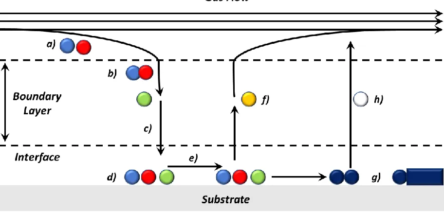
The sequence for CVD reaction involves several steps, beginning with vapor phase deliver to the
reaction chamber, proceeded by a series of quasi steady-state processes occurring at the substrate
the substrate called the “boundary layer” [15]. This sequence is schematically illustrated in Figure
1.4.
Figure 1.4. Schematic outline of a MOCVD process.
a) Precursor introduction: Precursor is introduced into the reaction chamber by an inert gas as a vapor.
b) Gas phase reactions: Depending on the precursor employed, reactions may occur in the gas phase, resulting in non-uniform nucleation and formation of powder on the surface.
The occurrence of this process should be reduced as much as possible to maintain film
uniformity.
c) Transfer of precursor to substrate: As the precursor crosses the boundary layer, the carrier gas transfers precursor vapor to the substrate surface. The gaseous layer between the
substrate and the position where the gas flow velocity is maximum, is called the boundary
layer. The rate of diffusion here depends on the total reactor pressure, temperature, and
concentration of precursor molecules in the gas phase present above the boundary layer.
e) Surface diffusion: Adsorbed precursor particles do not necessarily have to be static on the surface and have been shown to be mobile on the substrate surface. This is a factor that
may contribute to the growth of islands and particles during CVD.
f) Desorption of Precursor: Desorption and mass transport of decomposed precursor may occur on the surface and is dependent on surface functionality as well as precursor
reactivity.
g) Nucleation, island growth, and film growth: Surface chemical reaction leading to growth of islands and particles or film depending on surface reaction sites. Precursors either react
with neighboring molecules, with the substrate or with molecules in the gas phase to form
a film.
h) Desorption of volatile surface reaction products: Volatile reaction by-products and unreacted precursor molecules are pushed out from the reactor by carrier gas.
Growth of films by thermal CVD is determined by several different parameters including,
substrate temperature, reactor pressure, and gas-phase chemistry. The growth rate of films
produced using CVD can be limited by either surface reaction kinetics, or mass transport of
precursor to the substrate. Figure 1.5 presents an Arrhenius plot outlining the influence of
temperature on growth rate. Three different regions can describe this reaction process. The first
region is characterized by low temperatures and low pressures and is known as the precursor
depletion region and film growth is determined by surface reaction kinetics. With a lower reactor
pressure, a thin boundary layer is formed, and reactants can easily reach the surface. As
temperature increases film growth enters a diffusion controlled region where almost all precursor
molecules react to the substrate to form a film. This region is said to be independent of substrate
temperature and is a key component to achieving highly uniform and conformal films. Further
increasing the temperature results in a region controlled by reaction kinetics. As temperature and
pressure increases, a thicker boundary layer is formed and precursor diffusion to the surface
becomes difficult. Furthermore, diffusion of by-products produced at the surface becomes difficult
due to increased thickness of the boundary layer. Therefore, the rate of film growth is limited by
kinetic processes such as precursor adsorption, surface reactions and desorption of reaction
Figure 1.5. Arrhenius plot outlining the influence of temperature on growth rate of CVD films
[17].
1.4.4
Atomic Layer Deposition
Atomic layer deposition is an analogue of CVD but allows for increased control over film
thickness and provides enhanced film conformality over high aspect-ratio surfaces. In CVD, two
or more precursors are introduced simultaneously into a reaction chamber. ALD separates
introduction of precursor so each can react as two half reactions. By sequentially introducing
precursors into the reaction chamber, each precursor can chemisorb onto the substrate surface until
all reaction sites are consumed in a self-saturation process. Once all surface sites are saturated,
excess precursor and reaction by-products are removed with an inert gas using a purge step. This
is followed by introduction of a second reactant which can react to the chemisorbed precursor
initially introduced. This process continues until all reaction sites are consumed and self-saturation
is achieved. Another purge step is then performed to remove excess reactant and reaction
by-products, thus completing one ALD cycle. This pulse-purge-pulse-purge process, coupled with
self-saturating behavior, allows ALD to deposit thin film with angstrom level control. However,
in practicality, it is unlikely that a fully formed monolayer is deposited with each half cycle. For
this to happen several conditions need to be fulfilled, including ensuring precursor stability
throughout its introduction to the substrate and complete homogeneity of surface functionality. A
more accurate description of film morphology would be the deposition and nucleation of
nanoparticles or a partial coating which eventually stitches together over subsequent cycles [18].
number of ALD cycles employed. This is commonly referred to as growth per cycle (GPC). Figure
1.6 provides a schematic outline of a typical ALD process.
Figure 1.6. a) Flow process of ALD cycle consisting of two half steps with alternating cycles of precursor and reactant dosing separated by a purge step. b) Practical growth conditions for ALD of particles and thin films. c) Saturating pulse conditions to achieve self-limiting growth.
The reaction scheme outlined above is dependent on several physical properties including
precursor stability, reactivity, volatility, and reactor temperature. Precursor chemistry is crucial to
achieving good ALD of thin films and several precursor requirements need to be met. ALD
precursors must be thermally stable in the gas phase and not react with surrounding precursor
molecules, but still be reactive enough to undergo chemisorption on the surface. The precursor
must also be volatile and have a low melting point to allow for sufficient vapor to be drawn by the
vacuum during a pulse step. This can be achieved by choosing compounds that have a low
molecular weight and ligands with branching asymmetry that are coordinatively saturated to the
central atom. Another important for achieving a self-limiting monolayer by an ALD precursor is
steric protection of the central atom. This reduces chances for reaction to occur with other
precursor molecules in the gas phase [19]. The range of temperatures for which these properties
are favorable is known as the ALD window, as shown in Figure 1.7. If these stringent requirements
are not met decomposition of precursor in the gas phase may occur and result in higher than
Figure 1.7. Temperature dependence for the growth of ALD films.
The linear growth observed for ALD processes stem from self-limiting characteristics.
However, as mentioned earlier, the initial stages of ALD film growth is likely to occur in a
non-linear fashion. This is dependent on surface adsorption and reaction of precursor to the substrate
and is related to surface chemistry. With continued deposition, the effect of the original substrate
is lost and steady state growth can be achieved [20]. If GPC is higher for the first few cycles, this
growth is referred to as substrate-enhanced growth. If growth is initially impeded the GPC is
referred to as being substrate-inhibited. Finally, if the substrate has an insignificant effect on GPC,
then ALD proceeds in a linear fashion [21]. Nucleation of ALD is important for the deposition of
continuous pin-hole free films. A lack of uniform nucleation sites results in island like growth and
results in the deposition of nanoparticles (NPs) that follow a Volmer-Weber growth pattern [22].
This can be advantages for the deposition of NPs by ALD and fine tuning of this feature can allow
for NP growth on high aspect ratio structures. This is especially useful for the deposition of noble
Figure 1.8. Demonstration of substrate effect on growth rate.
Three chemisorption mechanisms can occur in an ALD reaction to achieve self-limiting
characteristics. This first is a ligand exchange reaction mechanism where the precursor molecules
(MLn) splits on the surface. The ligand (L) combines with a surface group ||-a to form a volatile
compound that can be purged away as by-product, aL. The remaining part of the molecule then
chemisorbs to the surface as a MLn-1 species. Ligand-exchange reactions can proceed for more than
one ligand and can also occur for adsorbed MLz species and surface groups. These reactions release
ligands as aL and consume additional ||-a groups, thereby reducing available sites for metals to
bond. The second type of self-limiting reaction is a dissociation reaction. This involves a splitting
of the reactant molecule between two reaction sites on the surface. Similar to the ligand exchange
reaction, dissociation may continue on the surface, but it does not affect the number of bonded M
atoms and the number of bonded ligands. The third type of reaction mechanism that can occur is
the association reaction. This reaction proceeds by forming coordinate bonds with reactive surface
sites. In association reactions there is no release of ligands [21].
Ligand Exchange: ||-a + MLn(g) ---> ||-MLn-1 + aL(g)
Dissociation Reaction: ||-a + ||-b + MLn(g) ---> ||-a- MLn-1 + ||-b- L
The growth mechanism in ALD is unique and different from both CVD and PVD. By
splitting the introduction of precursor into two separate self-saturating half reactions, film
conformality is greatly improved. Compared to PVD and CVD, which are considered line-of-sight
techniques, ALD is a non-line of sight technique that can conformally coat high aspect ratio
structures. Conformal step coverage occurs when reactants migrate rapidly after adsorption on step
surfaces. However, this comes with a penalty to deposition time. ALD deposition can range from
0.01nm/cycle to 1 nm/cycle, with cycle time being up to 2 min/cycle depending on ALD reactor,
substrate, and precursor used. ALD processes are typically used for the deposition of solid
inorganic materials. Materials by ALD are grown as oxides, nitrides, sulphides, selenides,
tellurides, pure elements, and others. Figure 1.10 presents an overview of all the inorganic
materials deposited using ALD.
Figure 1.9.Schematic diagram demonstrating film deposition using ALD on a structured substrate where deposition occurs uniformly across the surface.
1.4.5
Molecular Layer Deposition
Molecular layer deposition (MLD) is an extension of ALD and is used to deposit organic
materials. Similar to ALD, an MLD cycle is comprised of two precursor doses separated by
purge/evacuation step between each dose to remove excess precursor molecules as well as reaction
by-products. During each dose, a bifunctional precursor molecule reacts with the appropriate
surface groups. A key difference between ALD and MLD is the linking chemistry used. During
ALD, a metal precursor is reacted with another compound to remove ligands and regenerate
surface functionality. MLD utilizes various linking chemistries and is dependent on precursor
bifunctionality, which can be represented in an A-L-A and B-M-B format. In these precursors, “A”
and “B” are chemical functional groups, such as chlorides, amines, hydroxyls, carboxylic acids, and/or acid chlorides, while “L” and “M” are organic carbon-based fragments. Some of the first
organic MLD processes involved condensation polymerization reactions to form surface bonded
polymeric materials [23]. This versatile chemistry can be used to deposit thin conformal organic
polymers such as polyamides[24], polyimides[25], and polyureas[26]. Furthermore, some of these
organic precursors can also be mixed with the inorganic precursors from ALD to define a new
class of hybrid organic-inorganic material. For example, a metal alkyl, such as trimethylaluminum
(TMA), can react with a diol, such as ethylene glycol to produce an aluminum alkoxide species.
The metal alkyl molecule is described as MRx, while the diol is represented as HOR’OH. The
general MLD reaction can be written as, with * denoting a surface species [27]:
MR* + HOR’OH M-OR’OH* + RH
R’OH* + MR
x R’O-MR x-1* +RH
Hybrid organic-inorganic materials can provide precisely turned mechanical, optical, chemical and
electrical properties [28]. Development of new hybrid organic-inorganic materials is dependent on
the methods used to prepare these materials. Relatively simple inorganic-organic composite
materials may be used to create complex hybrid frameworks such as superlattices and
nanolaminates from alternating inorganic and organic layers [29]. Furthermore, these hybrid
organic-inorganic films have properties that range between pure organic and inorganic films and
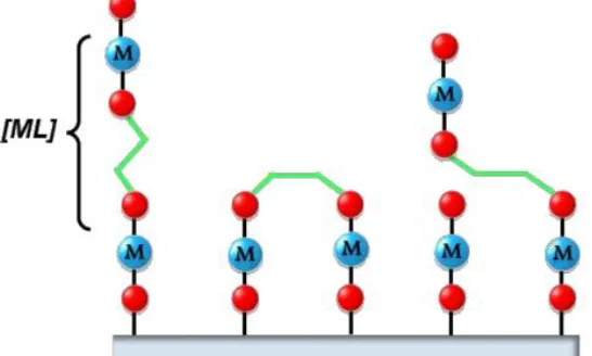
Figure 1.11.Schematic of MLD using bifunctional monomers with “triangular” or “square” functional groups [23].
Although the reaction schematic above presents the growth of MLD films as occurring linearly,
this is highly unlikely to be the case. The ideal growth rate of MLD films should then be equal to
the combined length of each organic precursor molecule. One reason for deviation from this
behavior is that organic precursor molecules with long chains are likely to tilt, resulting in film
growth that is not ideally perpendicular to the surface. Furthermore, steric hindrance of large
organic molecules results in decreased packing density and blocking of surface nucleation sites
[32]. Bifunctional precursor molecules, such as ethylene glycol, may bend and react twice with the
surface, reducing the number of reactive sites and resulting in decreased growth rate. Figure 1.12
Figure 1.12. Ideally, organic precursor molecules should react with only one surface site with film growth occurring vertically. However, molecules may react twice and polymer chain may
have tilt perpendicular to the surface [32].
MLD reactions have also been shown to have decreasing growth rate with increasing temperature
[33]–[35]. This temperature dependent behavior is attributed to the sticking coefficient (S0) of
precursors adsorbed on the surface. Additionally, diffusion out of the film is enhanced at higher
temperatures, resulting in a lower growth rate. The following equation can be used to describe this
phenomenon [36]:
S0 = a
[1 +kkd
r{exp(
Ed− Er
kT )}]
a =Trapping coefficient of the precursor kd = Rate of desorption of precursor
kr =Rate of reaction of precursor to substrate Ed= Activation energy for desorption
![Figure 1.1. Family tree diagram of common thin film deposition techniques [4]. Processes central to this thesis are highlighted in red](https://thumb-us.123doks.com/thumbv2/123dok_us/1932221.1253799/31.612.115.497.121.497/figure-family-diagram-deposition-techniques-processes-central-highlighted.webp)

![Figure 1.10. Table summarizing materials grown by ALD [21].](https://thumb-us.123doks.com/thumbv2/123dok_us/1932221.1253799/40.612.224.394.313.395/figure-table-summarizing-materials-grown-ald.webp)
![Figure 1.11. Schematic of MLD using bifunctional monomers with “triangular” or “square” functional groups [23]](https://thumb-us.123doks.com/thumbv2/123dok_us/1932221.1253799/42.612.145.467.68.269/figure-schematic-bifunctional-monomers-triangular-square-functional-groups.webp)