Available online: https://edupediapublications.org/journals/index.php/IJR/ P a g e | 1115 ABSTRACT: This paper presents the
design of a Hybrid logic level [H.L.L] multiplier for 32*32bit number multiplication. Modern computer system is a dedicated and very high speed unique multiplier. Therefore, this paper presents the design a Hybrid logic level multiplier. The proposed system generates M, N and interconnected blocks. By extending bit of the operands and generating an additional product the Hybrid logic level multiplier is obtained. Multiplication operation is performed by the Hybrid logic level is efficient with the less area and it reduces delay i.e., speed is increased.
Keywords: H.L.L, partial products, Hybrid level logic unit.
I.INTRODUCTION
In most signal processing algorithms multiplication is the fundamental operation. Multipliers have large area, long latency and consume considerable power. The important part in low-power VLSI system design is low power multiplier design. There has been extensive work on low-power multipliers at technology, physical, circuit and logic levels. A system’s performance is generally determined by the performance of the multiplier because the multiplier is generally the slowest element in the system.
Furthermore, it is generally the most area consuming .Hence, optimizing the speed and area of the multiplier is a major design issue. However, conflicting constraints are usually area and speed so that improving speed results mostly in larger areas. As a result, a whole spectrum of multipliers with different area-speed constraints has been designed with fully parallel.
For digital signal processing (DSP) applications such as for multimedia and communication systems the high speed multipliers and pipelined multipliers are used. High speed DSP computation applications such as Fast Fourier transform (FFT) require additions and multiplications.
II.LITERATURE SURVEY
An irregular partial product array is generated by the conventional modified encoding(MBE) Booth because of the extra partial product bit at the least significant bit position of each partial product row. A simple approach in paper [4] is presented to generate a regular partial product array with fewer partial product rows and negligible overhead, thereby reducing the area, lowering the complexity of partial product reduction delay, and power of MBE multipliers. But the drawback of this multiplier is that it function only for signed
Design an Aging Aware Hybrid Logic Level Multiplier
CHINTA JYOTHI PADMAVATHI
PG – SCHOLAR – VLSI Design Dept. of E.C.E
MALINENI LAKSHMAIAH WOMENS ENGENERING COLLEGE
GUNTUR DT.
KUNDURTHI RAVI KUMAR ASSOCIATE PROFESSOR
Dept. of E.C.E
MALINENI LAKSHMAIAH WOMENS ENGENERING COLLEGE
Available online: https://edupediapublications.org/journals/index.php/IJR/ P a g e | 1116 number operands.
FIG. 1: EXISTED SYSTEM
…….. ……. ….
The improvement on the normal array multiplier (AM) is by column-by passing multiplier. The multiplier array consists of (n−1) rows of carry save adder (CSA), in
which each row contains (n − 1) full adder
(FA) cells. Each FA in the CSA array has two outputs: 1) the sum bit goes down and 2) the carry bit goes to the lower left FA. The last row is a ripple adder for carry propagation.
N(31) N(30) N2 N1 N0
M0
M2 M1
M(16)
M(30)
M(31)
p
INPUTS
OUTPUTS
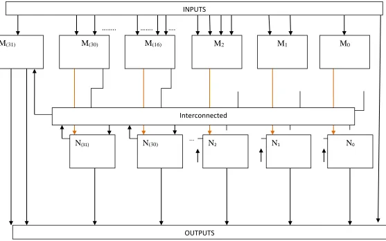
Fig. 2 32*32 HIGH PERFORMANCE HYBRID LOGIC
LEVEL MULTIPLIER Interconnected
Available online: https://edupediapublications.org/journals/index.php/IJR/ P a g e | 1117 III.PROPOSED SYSTEM
The gates in the Hybrid logic level [H.L.L] multiplier are always active regard of input logics. In, Hybrid logic level [H.L.L] multiplier design is proposed in which the operations are disabled if the corresponding bit in the multiplicand is 0. Fig. 2 shows a 32*32Hybrid logic level [H.L.L] multiplier, it can be seen that the M0, M1,…Mn done their operations and the outputs are passed to interconnected
FIG. 3 PROPOSED SYSTEM [4*4 D.L.L]
Block and N-Block simultaneously. Depends on the preference of operation the Hybrid level logic gives the N-block output to interconnected block and vice versa.
Therefore, the output of the adders in both diagonals is 0, and the output sum bit is simply equal to the third bit.The above fig. 3 shows the 4*4 high performance Hybrid logic level multiplierreduced the timing waste occurring in traditional circuits that use the critical path cycle as an execution cycle period. The basic concept is to execute a shorter path using Hybrid logic. Since
most paths execute in a cycle period that is much smaller than the critical path delay.
IV.RESULTS
To reduce the number of partial product rows to be added hybrid logic level has been adopted in multipliers, thus reducing the size and enhancing the speed of the reduction tree. The least significant bit position of each partial product row encoding, leading to an irregular partial product array and a complex reduction tree. Therefore, the Hybrid logic level multipliers with partial product array produce a very high speed.
The above fig. 4 shows the R.T.L schematic of high performance Hybrid logic level multiplier and fig. 5 shows the technical schematic one of the LUT block of high performance Hybrid logic level multiplier.
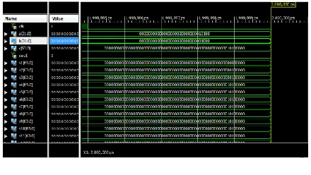
Available online: https://edupediapublications.org/journals/index.php/IJR/ P a g e | 1118 The below figure 6 shows the output
waveform of 32*32 bit Hybrid logic level multiplier.
The below table 1 shows the comparison of existed system 32*32 and proposed system 32*32 with area and delay
System/parameter Area[kb] Delay[ns]
Existed System 316352 126.865
Proposed system 272000 110.363
The above comparison table shows that area of the proposed system is less than existed system and delay is also efficient.
V.CONCLUSION
The proposed system generates M, N and interconnected block. The each block consists of gates and the row in the architecture is lesser than existed multiplier.
By generating a product with Hybrid logic level multiplier 32*32 is obtained. Multiplication operation is performed by the Hybrid logic level unit is better performance than existed multiplier. The required hardware and the chip memory reduces and it reduces delay i.e., speed is increased.
VI.REFERENCES
[1] R. Vattikonda, W. Wang, and Y. Cao, “Modeling and minimization of pMOS NBTI effect for robust nanometre design,”
in Proc. ACM/IEEEDAC, Jun. 2004, pp.
1047–1052.
[2] H. Abrishami, S. Hatami, B. Amelifard, and M. Pedram, “NBTI-aware flip-flop characterization and design,” in Proc. 44th
ACM GLSVLSI,2008, pp. 29–34
[3] S. V. Kumar, C. H. Kim, and S. S. Sapatnekar, “NBTI-aware synthesis of digital circuits,” in Proc. ACM/IEEE DAC, Jun. 2007, pp. 370–375.
[4] A. Calimera, E. Macii, and M. Poncino, “Design techniques for NBTItolerantpower-gating architecture,” IEEE Trans. Circuits Syst., Exp.Briefs, vol. 59, no. 4, pp. 249– 253, Apr. 2012.
[5] K.-C. Wu and D. Marculescu, “Joint logic restructuring and pin reordering
against NBTI-induced performance
degradation,” in Proc. DATE,2009, pp. 75– 80.
[6] Y. Lee and T. Kim, “A fine-grained technique of NBTI-aware voltage scaling and body biasing for standard cell based designs,” in Proc. ASPDAC,2011, pp. 603– 608.
FIG. 5 LUT IN TECHNICAL SCHEMATIC
Available online: https://edupediapublications.org/journals/index.php/IJR/ P a g e | 1119 [7] M. Basoglu, M. Orshansky, and M. Erez,
“NBTI-aware DVFS: A new approach to saving energy and increasing processor lifetime,” in Proc.ACM/IEEE ISLPED, Aug. 2010, pp. 253–258.
[8] K.-C. Wu and D. Marculescu, “Aging-aware timing analysis and optimization considering path sensitization,” in Proc. DATE, 2011, pp. 1–6.
[9] K. Du, P. Varman, and K. Mohanram, “High performance reliable variable latency carry select addition,” in Proc. DATE, 2012, pp. 1257–1262.
[10] A. K. Verma, P. Brisk, and P. Ienne, “Variable latency speculative addition: A new paradigm for arithmetic circuit design,”
in Proc. DATE,2008, pp. 1250–1255.
CHINTA JYOTHIPADMAVATHI studied B.Tech at Malineni
Lakshmaiah Women's Engineering College during (2010-2014). At present, she is pursuing M.Tech at Malineni Lakshmaiah Women's Engineering college . Her area of Interest is VLSI and Communications.
KUNDURTHI RAVI KUMAR studied B.Tech at Koneru
![FIG. 3 PROPOSED SYSTEM [4*4 D.L.L]](https://thumb-us.123doks.com/thumbv2/123dok_us/7771418.1279750/3.612.86.282.309.460/fig-proposed-system-d-l-l.webp)