Efficient FPGA implementations of volterra DFES for
optical systems
EMERETLIS, Andreas, KELEFOURAS, Vasileios
<http://orcid.org/0000-0001-9591-913X>, THEODORIDIS, George and GLENTIS, Othon
Available from Sheffield Hallam University Research Archive (SHURA) at:
http://shura.shu.ac.uk/18375/
This document is the author deposited version. You are advised to consult the
publisher's version if you wish to cite from it.
Published version
EMERETLIS, Andreas, KELEFOURAS, Vasileios, THEODORIDIS, George and
GLENTIS, Othon (2014). Efficient FPGA implementations of volterra DFES for
optical systems. In: 2014 IEEE Dallas Circuits and Systems Conference (DCAS
2014) : Conference theme: Enabling an internet of things – from sensors to servers.
Piscataway, NJ, IEEE.
Copyright and re-use policy
See
http://shura.shu.ac.uk/information.html
EF F ICIENT F PGA IMPLEMENTATIONS OF
VOLTERRA DF ES F OR OPTICAL SYSTEMS
A. Emeretlis, V. Kelefouras, G. Theodoridis
Department of Electrical and Computer Engineering, University of Patras,
Patras, Greece
{emeretlis, kelefouras, theodor}@ece.upatras.gr
G-O. Glentis
Department of Informatics and Telecommunications, University of Peloponnese,
Tripolis, Greece, [email protected]
Abstract— In this work suitable architectures and high-throughput FPGA implementations of Volterra Decision Feedback Equalizers (VDFEs) for optical communication links are presented. Two VDFE configurations were selected based on the available resources of the employed FPGA devices, and two multiplexer-based architectures were developed for each of them in order to achieve the target throughput. The comparison of the
experimental results with respect to different VDFE
configurations, throughput, and FPGA devices points out the
platform-specific design characteristics. The introduced
architectures meet the desired 10Gb/s throughput, so it is demonstrated that the FPGA is a suitable platform for high-speed optical fiber communication systems.
Keywords— Decision F eedback Equalizer, Volterra F ilters, F PGA, F iber Optical Communication Links.
I. INTRODUCTION
The use of optical communication systems is able to meet the growing demand for bandwidth as the data transmission rates increase. Thus, optical communication systems based on the Intensity Modulation/Direct Detection (IM/DD) have been used extensively for optical links. Although coherent optical systems achieve higher transmission rates, direct detection offers low-cost and simple receiver design, since the optical to electrical conversion is realized via a photo-detector, [1], [2].
Nevertheless, the limited capacity of the optical fibers causes important channel impairments that need to be overcome. The advance of the semiconductor technology has provided a means to electronically compensate all or a part of the Chromatic Dispersion (CD), thus reducing or even eliminating the costly optical compensation modules. This enables the use of high-capacity channels over long distances [1]-[3].
A widely used structure to suppress signal distortion in high-speed communication systems is the Decision Feedback Equalizer (DFE) [4]. It uses a Feed-Forward Filter (FFF) and a Feed-Back Filter (FBF) in order to cancel precursor and postcursor InterSymbol Interference (ISI), respectively (i.e. the overlapping between the current received symbol with previous and subsequent ones). However, in IM/DD systems, the conventional DFE, consisting of linear filters, is not able to efficiently mitigate the ISI, because the CD has a nonlinear
effect. In order to face the nonlinearities, the use of second order Volterra filters as FFF and FBF has been proposed [5], [6].
In hardware implementations of DFEs, the feedback loop limits the achievable frequency imposing an upper bound on the throughput [7]. To avoid this limitation, a multiplexer-based approach was proposed in [9], where the recursive scheme was reformulated eliminating the computational units from the feedback loop. Alternative approaches trying to reduce the hardware cost of the multiplexer-based method were presented in [10] and [11]. However, as they maintain all or a part of the computational units inside the feedback loop, which cannot be pipelined, they are not suitable for high-throughput FPGA implementations.
In this paper efficient pipelined and parallel architectures and high-throughput FPGA implementations of Volterra-based DFEs (VDFEs) are presented. Two particular VDFE configurations were implemented taking into account the FPGA-specific characteristics. For the design of the feedback loop the multiplexer-based approach was employed and adapted to the Votlerra filter. The introduced architectures fully exploit the platform-specific resources to produce high-speed implementations. Both of the architectures meet the target throughput of 10Gb/s, and they are able to achieve rates of 11Gb/s and 17Gb/s. Despite the significant increase of the complexity by the use of the Volterra filters, it is demonstrated that the FPGA technology can be used as a candidate platform to achieve high-speed implementations amenable for optical communication links.
The paper is organized as follows. In Section II the hardware architecture is presented. The algorithmic transformations are demonstrated and the employed FPGA-specific features are highlighted. In Section III the experimental results are provided and discussed. Finally, Section IV concludes the paper.
II. HARDWARE ARCHITECTURE
Let I(n) ∈ {0,1} be the transmitted binary sequence, Ts the
symbol period and y(t) the electrical signal produced at the receiver. In order the equalizer to be less sensitive to the
receiver’s sampling phase, fractional spacing is used, that is
two samples per symbol are processed. The Ts /2 Fractionally
Spaced (FS) Volterra equalizer aiming at recovering the transmitted information in the Non-return to Zero On/Off Keying (NRZ-OOK) optical communications system is described by the following equation.
1 2
1 2 1
1 2
1 2 1
1 2
1 0 1 1 2
, 1 2
1 0
, 1 2
1
( ) ( )
( ) ( )
ˆ( ) (ˆ )
f f f b b M i m i i m M M i
m m i i
i m m m M M
m m m m m
u n f y n m
f y n m y n m
b I n m I n m
(1)where y1(n) ≡ y(nTs+ Ts/4) and y2(n) ≡ y(nTs+3Ts/4) denote the
received FS signals, and Î(n) = Q(u(n)) is the received symbol, with Q(.) representing a decision device that maps the signal
u(n) into either “1” or “0”. Throughout this paper, the pair of
integers (Mf, Mb) is used to denote the orders of the the
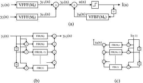
Feed-Forward (FF) and Feed-Back (FB) filters, respectively. The Signal Flow Graph (SFG) of the VDFE is depicted in Fig. 1a.
The FF part of the equalizer consists of two linear filters, with coefficients denoted by f 1m and f2m, and two second order
Volterra kernels, with coefficients denoted by f 1m1,m2andf
2 m1,m2
(Fig. 1b). The FB part comprises a second order Volterra kernel, with coefficients denoted by bm1,m2 (Fig. 1c). The linear part of the FB filter is incorporated in the diagonal of the corresponding second order Volterra kernel, because in this case Î2(n) = Î(n). This equalizer is denoted hereafter as VDFE(Mf, Mb).
To meet the high-throughput requirements of the optical communication systems, the application of the techniques of pipelining and parallelism is compulsory. However, due to the recursive nature of the equalizer, different approaches must be employed for the FF and FB sections.
A. FF Transformations
The FF part can be easily pipelined by inserting registers
between the filters’ components (adders, multipliers). The
synchronization between the parallel data-paths from the input to the output is guaranteed if the same amount of delays is inserted in all data-paths [8]. The parallel structure of the FF Volterra filter can be derived by unrolling the first two terms of (1) so that all the parallel outputs are described. Alternatively, the parallel FIR filters can be developed
separately and then connected properly to form the parallel Volterra filters.
B. FB Transformations
The application of pipelining is not straightforward in the case of the FB loop of the equalizer, since the direct insertion of pipeline registers in the loop alters the implemented algorithm by changing the transfer function of the system. Moreover, due to the quantization of the summed output u(n) of the FF and FB filters, the output Î(n) of the equalizer cannot be directly expressed as a function of the previous outputs, generating a loop with large computational delay after unrolling the equation that describes it.
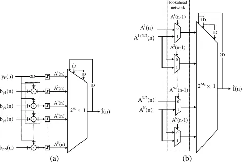
To overcome the above limitations, a multiplexer-based approach is employed [9]. This approach exploits the specific property of the DFE that the output value of the quantizer
equals to one of a set of predetermined values (“0”, “1”). As
the output of the quantizer is fed to the FBF, all the possible output values of the FBF can be precomputed. This assumes that the equalizer is not adaptive, which means that the values of the coefficients of the FBF are fixed and known. In the case of the Volterra filter, the inputs of the FIR filters also have binary values, since the multiplication of the fed-back binary outputs correspond to the operation of logical AND.
After the addition of the precomputed values with the output of the FF part and the quantization of the result, the possible output values of the equalizer become available. Then, the proper one is selected based on the previous equalizer outputs using a multiplexer (Fig. 2a). In this structure, the components that perform arithmetic operations are not included in the feedback loop, which contains only a 1-bit 2Mb-to-1 multiplexer; thus, they can be easily pipelined. The values bpi, i=1, 2, …, N, where N=2Mb, correspond to all
the possible values of the output yB(n) of the FBF. In the case
of the Volterra filter they involve coefficients from all the FIR filters of the FB Volterra kernel. Also, the dashed blocks correspond to FPGA specific blocks and are discussed in the following subsection.
The parallel architecture of the reformulated feedback structure is derived by applying the lookahead transformation [9]. This transformation adds registers inside the multiplexer loop at the expense of lookahead stages consisting of 2-to-1 multiplexers (Fig. 2b). After unrolling the pipelined structure, the inner delays are distributed inside the parallel multiplexer loop. Hence, if the number of delays inside the initial loop equals to the applied parallelism, the unfolding results in a fully pipelined loop, having one register between the parallel multiplexers. So, the amount of lookahead stages corresponds to the number of the required parallelism.
When the number of the parallel data-paths is greater than the order of the FBF, a low-complexity DFE architecture based on incremental block processing can be employed [12]. According to this approach, for a parallel ×L architecture of a Mb-th order filter, the first Mb outputs are produced in parallel
while the L-Mb outputs are calculated directly from the
previous ones, eliminating the lookahead stages and resulting in area reduction. In this work both the straightforward and the incremental approaches are considered.
y1(n) VFFF(Mf)
VFBF(Mb)
+ Î(n)
yF(n)
yB(n)
u(n)
D
+
y2(n) VFFF(Mf)
yF1(n)
yF2(n)
(a)
FIR(Mf) FIR(Mf)
FIR(Mf -1)
×
y2(n)
×
D
yF2(n)
+ + + FIR(1) × D + + + × × D
Î(n-1)
yB(n)
×
D
+
FIR(Mb) FIR(Mb-1)
FIR(1)
[image:3.612.56.288.56.191.2](b) (c)
C. FPGA Design Particularities
To achieve a high-performance implementation the specific DSP-oriented features of the Xilinx FPGA devices were fully exploited. The dedicated hardware block for performing arithmetic operations in Xilinx FPGAs is the DSP48E1 slice [13]. It mainly consists of a 25×18 bits two’s complement multiplier followed by a 48-bit accumulator, which can be used separately, along with internal pipeline registers. To operate at full speed, the use of the adder requires two pipeline registers, placed in the adder’s input and output. However, as the adder cannot be bypassed, the multiply or multiply-add operations require additionally one register between the multiplier and the adder.
When the adder is used separately, it is able to operate in Single Instruction Multiple Data (SIMD) mode, as dual 24-bit or quad 12-bit adder. In our case the required wordlength to satisfy the system specification in terms of BER is 14 bits, which was derived after extensive simulations. So, in the precomputation stage, one DSP slice is used to perform three 14-bit additions, as depicted by the dashed block in Fig. 2a. The management of the finite arithmetic was done manually by properly aligning the operands and deriving the result.
The DSP slices are located in columns across the device and dedicated high-speed interconnections exist in each column for cascading two DSP slices. Also, to operate at high-speed, only one register can be used between two cascaded DSPs [13]. Thus, this scheme was used for implementing the FIR filters.
On the other hand, the multipliers and adders, which
provide the filter’s inputs and sum their outputs (Fig. 1), are
also implemented in DSP slices but they use fabric interconnections. This happens because the second input of the DSPs of these components is provided by fabric interconnection. Hence, to improve the delay, this input must be registered, while one or more extra registers are needed on the routing line. However, in that way, the first input of the DSP slice is coming through the high-speed interconnection line having one register in this line, while the second input is provided via the fabric interconnection employing more than
one registers making the correct synchronization of these inputs impossible.
III. EXPERIMENTAL RESULTS AND DISCUSSION
The presented architectures were described through a parametric VHDL model. The correct functionality was verified through extensive Post Place & Route simulations and comparisons with a reference fixed-point MATLAB model using various input vectors produced by the simulation model of the optical transmission channel. The devices chosen for the implementation of the designs were the Xilinx FPGAs XC6VSX475T and XC7VX485T. As it is the first time that such systems are implemented on a FPGA, any comparison with other similar designs cannot be performed.
According to the available DSP resources, two VDFE configurations among the efficient VDFEs proposed in [6] were selected, namely the VDFE(5,3) and VDFE(7,4). Also, three throughput targets (5, 7, and 10Gb/s) were set in order to study the scalability of the designed architectures, which correspond to the first column of TABLE I for both FPGA devices (Virtex-6 – V6, Virtex-7 – V7). The second column corresponds to the employed parallelism and the total latency in clock cycles, while the other two columns present the utilized area by means of fabric resources and DSP slices.
From the implementation results it can be observed that the majority of cases achieves the target throughput with the same number of parallel data-paths. Consequently, the achievable frequency is the same for all the counterpart designs. This is caused by the inability of the designed architectures to fully exploit the dedicated DSP interconnection resources, even though all the components that perform arithmetic operations were mapped on DSP slices, as discussed in subsection II.C.
Moreover, the DSP interconnection delay is affected by the amount of logic implemented in fabric. When this amount is small, the placement of the fabric components and the fabric pipeline registers between the DSP slices is more efficient. Thus, the design achieves the target throughput with smaller parallelism. On the other hand, for larger designs, further pipelining the interconnection lines of the incoming and outgoing signals of the DSP slice makes the design more complex, leading to even larger routing delay.
Comparing the straightforward and the incremental approaches, it is derived that the parallelism and thus the frequency is the same for the majority of cases. As a result, the number of utilized DSP slices is equal in both approaches for those cases. However, because of the large computational delay of the incremental computation block, this approach requires more pipeline registers to operate at the same frequency as the straightforward one. In other words, the area cost of the pipelining compensates for the lower complexity of the incremental approach, resulting in designs of similar fabric area utilization. Nevertheless, for large parallelism, the use of incremental processing reduces the occupied slices at the expense of larger latency. The above is a specific feature of FPGAs. In contrast, in ASICs, less registers are needed as the
+
+ +
+
2D
yF(n) bp1(n) bp2(n) bp3(n)
bpN(n)
Î(n) 1D 1D
1D
2Mb1 A1(n)
A2(n)
A3(n) A4
(n)
AN (n)
0 1
0 1 A1
(n)
A1+N/2
(n)
A1(n-1)
A2(n-1)
0 1
0 1 AN/2
(n)
AN
(n)
AN-1(n-1)
AN(n-1) 2Mb 1
Î(n)
2D 1D
1D lookahead
network
[image:4.612.49.289.59.219.2](a) (b)
routing delay is not so important and the incremental approach always outperforms the straightforward one in terms of area.
In the case of the VDFE(5,3) implemented on Virtex-7 for the targets of 5 and 7Gb/s, the area reduction due to the use of incremental computation facilitates the placement and routing of the architecture’s components, allowing to achieve the target throughput with smaller parallelism. However, for the case of 10Gb/s, the reduction is not sufficient to decrease the routing delay. The same holds for the implementation of the VDFE(5,3) on Virtex-6, since the area reduction is not enough to influence the mapping procedure on a smaller device. On the contrary, comparing the straightforward parallel approach of VDFE(5,3), the Virtex-7 implementation achieves 5Gb/s with lower parallelism than the Virtex-6 one.
As the design grows either due to the increase of the
parallelism or the filters’ orders, the use of a larger device
cannot provide better performance in terms of frequency. Thus, the occupied area by the counterpart designs on different platforms is owing to the difference in the amount of pipeline registers, since the parallelism is the same. Nevertheless, the increase of the available DSP resources makes the Virtex-7 FPGA a suitable platform for the implementation of the VDFE(7,4) for 10Gb/s, which cannot be achieved on the Virtex-6 device. Furthermore, after occupying almost all the available DSP slices of the Virtex-7 device, the achieved throughput of the VDFE(5,3) and VDFE(7,4) was 17Gb/s and 11Gb/s, respectively.
IV. CONCLUSION
In this paper efficient FPGA implementations of two Volterra-based DFEs have been presented. The architectures were implemented in different FPGA devices and the design and platform particularities were demonstrated. Based on the
experimental results, it is proved that the introduced architectures are suitable for optical communications systems with data rates of 10Gb/s and beyond.
REFERENCES
[1] G. Agrawal, Fiber Optic Communication Systems, Wiley, 2012. [2] I. Papagianakis et al, Electronic channel equalization techniques,
Towards Digital Optical Networks, pp. 23-47, Springer, 2009. [3] A. Singer, N. Shanbag, and H. Bae, “Electronic dispersion
compensation,” IEEE Signal Proc. Magazine, pp. 110–130, Nov. 2008. [4] C. A. Belfiore and J. John H. Park, “Decision feedback equalizer,” IEEE
Trans. Commun. Technol., vol. 67, no. 8, pp. 1143–1156, 1979. [5] C. Xia and W. Rosenkranz, “Nonlinear electrical equalization for
different modulation formats with optical filtering,” J. Lightwave Tech., vol. 25, no. 4, pp. 996–1001, April 2007.
[6] G. O. Glentis, K. Georgoulakis, C. Matrakidis, “Performance evaluation of Decision Feedback Equalizers in fiber communication links” Int. Symp. on Communications, Control and Signal Processing, 2014. [7] M. Renfors and Y. Neuvo, “The maximum sampling rate of digital
filters under hardware speed constraints,” IEEE Trans. Circuits Syst. II, vol. 28, pp. 196–202, 1981.
[8] K. K. Parhi, VLSI Digital Signal Processing Systems: Design and Implementation, Wiltey, 1999.
[9] K. K. Parhi, “Design of multigigabit multiplexer-loop-based decision
feedback equalizers,” IEEE Trans. VLSI Syst., vol. 13, no. 4, pp. 489– 493, 2005.
[10] C.-H. Lin, A.-Y. Wu, and F.-M. Li, “High-performance VLSI
architecture of decision feedback equalizer for gigabit systems,” IEEE
Trans. Circuits Syst. II, vol. 53, pp. 911–915, 2006.
[11] Yu-Chun Lin; Muh-Tian Shiue; Shyh-Jye Jou,, "10Gbps decision feedback equalizer with dynamic lookahead decision loop," in Int Symp. on Circuits and Systems (ISCAS),pp.1839,1842, 2009.
[12] D. Oh and K. K. Parhi, “Low complexity design of high speed parallel
decision feedback equalizers,” IEEE Conf. on Application-Specific Systems, Architectures and Processors (ASAP), pp. 118–124, Sep. 2006 [13] Xilinx Inc., “7 Series DSP48E1 Slice”, User Guide, Available:
http://www.xilinx.com/support/documentation/user_guides/ug479_7Seri es_DSP48E1.pdf. Accessed: August 2014
TABLE I. IMPLEMENTATION RESULTS FOR VDFE(5,3)WITH
STRAIGHTFORWARD PARALLELISM
TABLE II. IMPLEMENTATION RESULTS FOR VDFE(5,3)WITH
INCREMENTAL PROCESSING
Throughput [Gb/s]
Parallelism/ Latency
Area
Slices DSPs
5 12/37 3,781 744 V6
7 16/44 7,629 992
10 24/52 12,787 1,488
5 11/27 3,021 682 V7
7 16/45 6,889 992
10 24/54 13,023 1,488
Throughput [Gb/s]
Parallelism/ Latency
Area
Slices DSPs
5 12/35 3,537 744 V6
7 16/58 7,022 992
10 24/62 9,996 1,488
5 10/42 3,068 620 V7
7 15/56 4,543 930
10 24/62 10,200 1,488
TABLE III. IMPLEMENTATION RESULTS FOR VDFE(7,4)WITH
STRAIGHTFORWARD PARALLELISM
TABLE IV. IMPLEMENTATION RESULTS FOR VDFE(7,4)WITH
INCREMENTAL PROCESSING
Throughput [Gb/s]
Parallelism/ Latency
Area
Slices DSPs
5 12/42 9,538 1,224 V6
7 16/44 12,528 1,632
10 N/A1 N/A1 N/A1
5 12/41 8,878 1,224 V7
7 16/43 12,461 1,632
10 24/60 22,743 2,448
Throughput [Gb/s]
Parallelism/ Latency
Area
Slices DSPs
5 12/50 9,134 1,224 V6
7 16/64 13,243 1,632
10 N/A1 N/A1 N/A1
5 12/50 9,022 1,224 V7
7 16/56 12,162 1,632
10 24/69 18,555 2,448
1.