Concurrent Dual-Band Power Amplifier Using Coupling
Matching Network for 60 GHz WPAN Applications
Hanieh Aliakbari1,*, Abdolali Abdipour1, Rashid Mirzavand2
1Microwave/mm-Wave & Wireless Communication Research Lab, Radio Communication Center of Excellence,
Electrical Engineering Department, Amirkabir University of Technology (Tehran Polytechnic), Tehran, Iran
2Intelligent Wireless Technology Lab, University of Alberta, Edmonton, Canada
Abstract
A new fully-integrated concurrent dual band CMOS power amplifier (PA) which covers the first and third channels of IEEE 802.15.3c standard is presented. In order to achieve concurrent operation of the 60 GHz PA in two desired narrow frequency bands, the multi-frequency passive coupling matching networks design is proposed. The full wave electromagnetic analysis (by the conventional Method of Moments (MOM)) and circuit analysis (using Circuit Envelope (CE)) are performed for the passive and active parts, respectively, in order to completely characterize the PA structure. This PA model has also been used in system level simulations. The results have shown two fractional bandwidths of 5% and 3%,P1dB of 8.8 dBm and 7.9 dBm at 58.32 and 62.64 GHz, respectively. Maximum power added efficiency (PAE) of 13% is
achieved in both targeted bands. Performance of this PA shows promising availability in the future dual band WPAN applications.
Keywords
Dual band, Nonlinearity, Power amplifier (PA), 60 GHz1. Introduction
The federal communications commission (FCC) allocates 7 GHz frequency band from 57 GHz to 64 GHz for unlicensed use over the United States which covers the three channels of the IEEE 802.15.3c standard. In the context of high data rate wireless personal area networks (WPANs), which is the class of networks with a range below 10 m [1]; new consumer-oriented applications are emerging. Some radio frequency component design according to dual band scenarios have been suggested in 60 GHz frequency band. One of these dual band approaches is to operate the 60 GHz system in combination with a system that works at a lower [2] or higher frequencies [3]. Due to the minimum bandwidth requirement of about 2 GHz for 60GHz devices [1], allocation of two carrier channels using different classes for two WPAN high data rate arbitrary scenarios, in one transmitter architecture, is suggested. Our dual-band design, which is within 60 GHz band (Figure 1), is primarily motivated by future applications in indoor home and office networks.
Power Amplifiers (PAs) are the most important blocks in RF front ends. Recently, several 60 GHz CMOS power amplifiers, which cover more than the three defined channels in 60 GHz band, are reported [4- 8]. By the way, the
* Corresponding author:
[email protected] (Hanieh Aliakbari) Published online at http://journal.sapub.org/msse
Copyright © 2015 Scientific & Academic Publishing. All Rights Reserved
In order to improve the accuracy of the passive models in this frequency and evaluate the nonlinearity behavior of the PA the hybrid analysis consisting of full wave electromagnetic analysis (MOM) and circuit analysis (CE) is performed [13]. In circuit envelope analysis the circuit model of the PA has been used instead of behavior models in order to obtain more accurate results [14]. The PA non-linearity impact is assessed by the maximum transmit power that can be maintained by the communication system while simultaneously meeting both the error vector magnitude (EVM) and transmit spectrum mask (TSM) requirements which are based on IEEE 802.15.3c standard. To the best of the author’s knowledge, this is the first reported dual band CMOS power amplifier that works concurrently within the 60 GHz standard band.
Figure 1. Frequency band allocation
2. 60 GHz Dual Band PA Design Method
Figure 2 shows the block diagram of the proposed concurrent dual band 60 GHz PA. It consists of both passive and active sections. Two stage active portions have a role of providing power gain in the desired frequency band and passive portion provide matching and multi-band requirements, simultaneously. The design of the passive sections is based on input, inter stage and output matching networks which combine the conventional and coupling structures for providing dual band characteristic. Cascode topology is employed in active portion since it has better isolation and stability rather than common source stage [4]. Limited maximum available gain (MAG) is one of the problems of power amplifiers at 60 GHz which could be solved by choosing proper classes like A or AB. On the other hand, the transistor current density bias of about 0.3 mA/μm could help the transistor to operate in optimal linearity and peak fmax [5]. These considerations resulted in the single transistor bias at Vdd=1.2V and Vgs= 0.7V. The nonlinear transistor model used in this paper is based on 90nm CMOS BSIM which is modified to consider the high frequency parasitic effects of the device.
2.1. Output Stage
The output matching network has a role of providing the optimum load for the second cascode stage in two desired
frequency bands. In order to achieve the maximum output power in two desired bands finding optimum output impedance is essential. For this purpose the load pull simulation which is consisting of third order harmonic balance (HB) analysis (K=4), is employed for one stage cascode. Actually in this load pull simulation the passive losses have not been considered. Simulation results shows that due to the close middle channel frequencies optimum loading conditions for each band is almost similar (ZL1=21.49 +j21.49 Ohm and ZL2=16.76+j22.91 Ohm at the first and second bands, respectively). So the output matching network which consists of two series and parallel 50 Ohm lines and one structure for selecting two bands will be evident.
Figure 2. Block diagram of the proposed concurrent dual band 60 GHz PA
Because of the small fractional bandwidth in each band (3%) coupling structure is utilized instead of conventional dual band matching network structures which are usually designed to achieve moderate-wide stop bands [16, 17]. By the idea of a coupled line structure, which is suitable for narrow band stop behavior, the output matching network can be optimized for realizing optimum load impedance in two frequency bands, simultaneously. The utilized structure is a half wave-length (λ/2) resonator edge-coupled to a 50 Ohm transmission line with a stepped-impedance distribution, as shown in Figure 3. The weak coupling between adjacent resonators at center provides flexible tuning of the narrow bandwidth. Stop-band behavior is obtained because of impedance mismatch over the middle frequency band. In order to improve the band stop behavior, four transmission zeros can be generated in middle band by cascading four unit-cells together. Furthermore, transmission zeros are created because of destructive interference of the signals propagating through the two paths and, as a result, sharp rejection characteristics are obtained.
To prevent currents from injecting into the substrate and, hence, reduce the transmission loss, a ground plane is placed above the Si substrate. Ground plane is placed at the bottom metal (M1) to prevent external loss of close proximity of the ground plane to the signal line.
Full wave simulation results show four transmission zeros in 59.63, 60.23, 60.68, 61.25 GHz frequencies. The final results will be demonstrated in section 2.3.
57 58 59 60 61 62 63 64
(GHz)
1st Band 2nd Band
57.24-59.4 GHz 61.56-63.72 GHz
Active Section
Dual Band 60 GHz Concurrent
PA
Channel1 Channel3
Active Section
Passive Section (Dual Band Matching
Network)
Figure 3. Half wave-length (λ/2) resonators edge coupled to a through 50
Ohm line utilizing in an output stage
2.2. Input Stage
In order to match the power amplifier to an input 50 Ohms and increase the power gain, an input stage is added to the power amplifier structure. Furthermore to keep away the interferences and isolate out band signals, adequate selectivity of about 7 GHz is needed for 60 GHz power amplifiers. From this point of view, matching to the 50 Ohm and narrow band pass filtering (~0.12) will be the defined role for input matching network.
In the same way as output matching network, the coupling structure is utilized in an input matching network. In order to
provide better performance the simple square patch on M7
layer is considered as a resonator due to the advantage of lower insertion loss in narrowband operation and higher power handling capability in comparison with line based resonators [18], which is in high importance in millimeter wave region. As illustrated in Figure 4 coupling to and from the resonator is facilitated by capacitive microstrip gaps. The axes of coupling to the resonator are orthogonal, so each couples energy independently to and from only one of the two orthogonal modes. Coupling to the resonator can be tuned for achieving narrowband operation of about 10%. By cutting away the corner geometry of the patch resonator two degenerate modes will be coupled. The initial dimension of the square patch will be:
reff L
c F
F
ε
2 01
10 = = (1)
As can be seen in Figure 4 the current distribution of the
fundamental modes (TMz
10 and TMz01) are orthogonal, so vertical and horizontal slots affect these degenerate modes, respectively.
By utilizing this technique, the coupling coefficient between two orthogonal modes can be tuned and the resonance frequencies will be separated. By optimizing W1,2
and L1,2 the trade-off will be done between lower 3 dB
bandwidth and higher insertion loss in the pass band.
Impedance matching between 50 Ohm feeding port and
coupling resonator structure has been achieved by a simple LC network.
Figure 4. Example of an image with acceptable resolution
This procedure results in the dual-mode input matching network which can generate two transmission zeros near the side of the pass band within 52 and 70 GHz. Finally, the interstage matching network is added to deliver maximum power from the output of the first stage to the input of the second stage:
. 1 *
1 in out =Γ
Γ (2)
2.3. Final Circuit (Harmonic Balance and Small Signal Characterization)
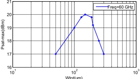
In this work, the proposed dual band matching network design technique was applied to the two stage power amplifier.Due to the parasitics in 60 GHz achieving a higher maximum output power by increasing the transistor width is not accessible (Figure 5). Therefore, by considering the technology limitations, the width and number of fingers in the output stage transistors have been fixed at Wg=3μm and Nf2=32, respectively. In order to have a better PAE, the number of fingers in the input stage transistors have been selected as Nf1=26.
Figure 5. Output power versus transistor width obtained by load pull simulations
Resonator
50 ohm-line Weak Coupling
Sg
50 Ohm Line 1st Coupled
Resonator
2nd Coupled Resonator
TMZ1,0,0
TMZ0,1,0
L
Coupled Resonator
port1
port2
W1
W2
L2
L1
Coupling excitation Matching Net
101 102 103
16 17 18 19 20 21
Wtot(um)
P
sa
t-m
ax
(d
B
m)
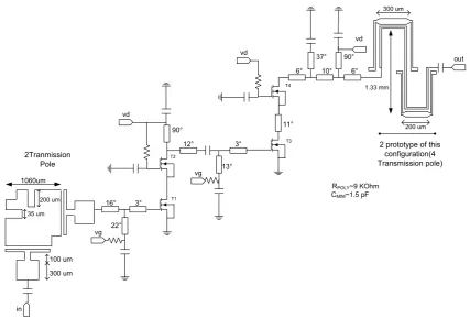
Figure 6. Concurrent dual band PA structure
Finally, the realized concurrent dual band PA is reported in Figure 6. By the circuit and layout co-simulation the small and large signal characterization will be done. Dual-band performance is clearly visible with insertion gain peaks around the two bands of interest and attenuation in between (Figure 7). The resulting S-parameter data show that the PA could work in 58.32 and 62.64 GHz bands with the insertion gain of 17 and 15.5 dB respectively. This structure produced six transmission zeros located in 52, 59.63, 60.23, 60.68, 61.25 and 69.60 GHz frequencies. Over all of the frequency range, the PA realizes input return loss S11 of smaller than -10 dB and the S12 results shows the unilateral behavior of the PA in the desired bands.
Figure 7. The simulated scattering parameters of the dual band PA
The nonlinear single tone results were achieved by 3rd
order harmonic balance (HB) simulation. The simulated
behavior of the nonlinear figure of merits (FOMs) as a function of frequency is reported in Figure 8 at 4dBm input power. If a variation of 1 dB is accepted on the output power, the two fractional bandwidths around 58.32 and 62.64 GHz result in 5% and 3%, respectively.
Figure 8. The simulated behavior of the nonlinear figure of merits (FOMs) versus frequency at 4dBm input power
The comparison between output power, gain, and efficiency behavior as a function of input power in two bands is reported in Figure 9 which shows almost little difference. Figure 9 shows PAEmax of 13%, P1dB of 8.8 dBm and PAEmax in
vd
vg
vg
vd
16°
22° 3°
90° 12°
13° 3°
11° 6°
37° 10°
90° 6°
out vd
RPOLY~9 KOhm
CMIM~1.5 pF T1
T2
T3 T4
1060um
300 um 100 um
200 um
35 um
1.33 mm 300 um
200 um
2 prototype of this configuration(4 Transmission pole) 2Tranmission
Pole
50 55 60 65 70 75 80
0 20 50
Pout
(d
B
m
) &
G
ai
n(d
B
)
50 55 60 65 70 75 80-20
0 20
Frequency(GHz)
PAE(
%
)
of 13%, P1dB of 7.9 dBm at 58.32 and 62.64 GHz, respectively.
Figure 9. FOMs as a function of frequency in two bands
The two tone harmonic balance (HB) simulation results reveal 17 and 18dBm of OIP3for center frequencies of 58.32 and 62.64 GHz respectively and a tone-spacing of 40 MHz.
3. Single Carrier Characterization
As indicated in IEEE 802.15.3c standard draft [1], a total of three Physical layers (PHYs) are defined for the mmWave PHY. They are as follows:
a) Single Carrier mode (SC PHY) b) High Speed Interface mode (HIS PHY) c) Audio/Visual mode (AV PHY)
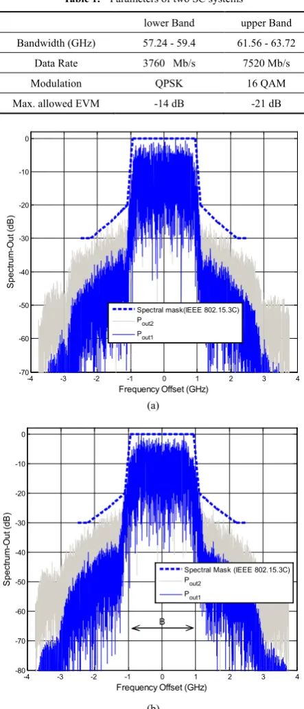
The HSI PHY and AV PHY (HRP, LRP) modes use orthogonal frequency domain multiplexing (OFDM). OFDM systems have higher peak-to-average power ratio (PAPR) than single carrier (SC) systems, thus power amplifier (PA) back off required to keep signal distortions due to PA non-linearity below the maximum allowed level in SC systems are typically lower, which results in higher PAE [19]. This section presents results of the PA non-linearity investigation for SC system in dual band 60 GHz WPAN scenarios. The single carrier mode in mm wave PHY (SC PHY) provides three classes of modulation and coding schemes (MCSs) targeting different wireless connectivity applications which occupy at least one channel bandwidth (~1.88 GHz) [1]. In this work the second and third SC class which support more than 1.5 Gb/s data rate has been used for driving 60 GHz power amplifier in each of the desired bands, respectively. This evaluation can be used for various data rate, dual band WPAN applications. A summary of SC systems parameters and requirement used in this work for PA non-linearity impact analyses are given in Table 1.
In order to analyze PA nonlinearity at system level the circuit model of the PA in addition to full wave electromagnetic model of passive section has been utilized
instead of behavioral models which can be result in more accurate results. Furthermore, circuit envelope method is used to analyze the nonlinear behavior of dual band 60 GHz PA in CMOS technology when driven by non-constant envelope signals. Circuit envelope technique can be named dynamic harmonic balance (HB) analysis, since handles the high-frequency dynamic of a modulated signal by steady-state CAD techniques such as harmonic balance (HB) simulation, and the low-frequency dynamic by time domain approaches.
Table 1. Parameters of two SC systems
lower Band upper Band Bandwidth (GHz) 57.24 - 59.4 61.56 - 63.72
Data Rate 3760 Mb/s 7520 Mb/s
Modulation QPSK 16 QAM
Max. allowed EVM -14 dB -21 dB
(a)
(b)
Figure 10. Spectral regrowth phenomenon (Pout2>Pout1) in (a) first and (b)
second band
-30 -25 -20 -15 -10 -5 0 5 10
-15 -10 -5 0 5 10 15 20
Pin(dBm)
Pout
(d
B
m
) &
G
ai
n(d
B
)
Channel 1 Channel 3
-30 -25 -20 -15 -10 -5 0 5 100
2 4 6 8 10 12 14
P
A
E
(%
)
-30 -25 -20 -15 -10 -5 0 5 100
2 4 6 8 10 12 14
Pout Gain
-4 -3 -2 -1 0 1 2 3 4
-70 -60 -50 -40 -30 -20 -10 0
Frequency Offset (GHz)
S
pec
trum
-O
ut
(dB
)
Spectral mask(IEEE 802.15.3C) Pout2
Pout1
-4 -3 -2 -1 0 1 2 3 4
-80 -70 -60 -50 -40 -30 -20 -10 0
Frequency Offset (GHz)
S
pec
trum
-O
ut
(dB
)
Spectral Mask (IEEE 802.15.3C) Pout2
Pout1
Figure 10(a), (b) shows the spectral regrowth phenomenon originating in nonlinear PA under two different OBOs in each band. It can clearly be seen that the spectral regrowth in out-of-band regions is below the TSM defined in the IEEE 802.15.3c standard. The estimated values of the power
amplifier OBOmin needed to meet the requirements on the
transmit spectrum mask are 4 and 3.8 dB, in each band, respectively which corresponds to Pout2.
It is well known that the EVM and TSM requirements have to be met by the communication system simultaneously. The requirements for maximum allowable EVM level depend on the class type used by the communication system (Table 1). The constellation of QPSK and 16-QAM signal after nonlinear amplification in each band under 4 and 3.8 dB OBO are shown in Figure 11(a), (b). It can also be seen that the outer points appear in a ring shape, which arises from the nonlinearity effects of a power amplifier. The average EVM is about 8% and 9%, which is under the standard limit of standard.
(a)
(b)
Figure 11. The constellation diagrams of (a) QPSK signal in first band under 4dB OBO, (b) 16-QAM signal in second band under 3.8dB OBO
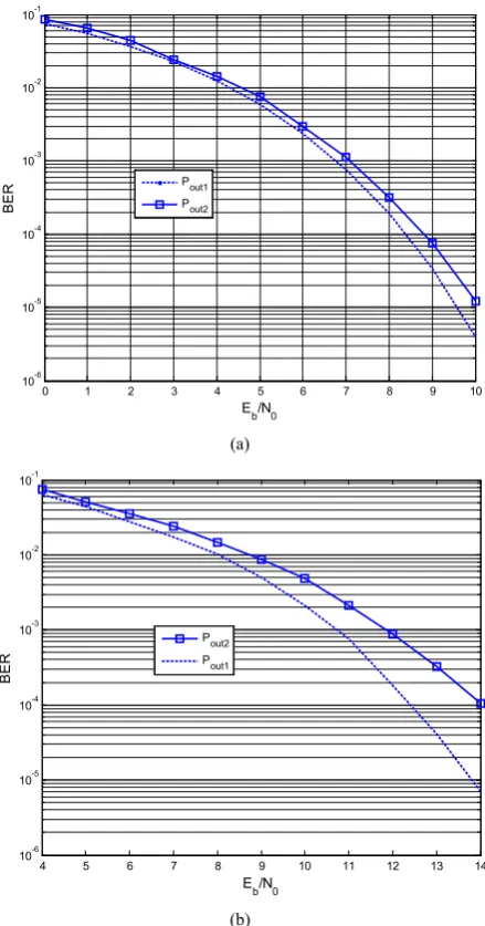
Another conventional performance measure for a digital communication system is the bit error rate (BER), which is usually a decreasing function of Eb/N0. The co-simulation for investigating the PA non-linearity effects on BER results is done by passing the modulated signal through the nonlinear
amplifier and an additive white gaussian noise (AWGN) channel. The same as before two different input levels have been tested for PA in each band which shows the degradation performance due to the PA nonlinearity (Figure 12).
(a)
(b)
Figure 12. BER results of two different Pout level in the (a) first and (b)
second band
4. Conclusions
In this paper, design and analysis of a 60 GHz two-stage dual band PA is presented
.
For the realization of narrowband operation in both bands the dual band coupling structure in matching networks was utilized. Standard 90 nm-CMOS process was used for the analysis and design of the PA operating concurrently at the first and third channels in the IEEE 802.15.3c standard definition. The small signal and single carrier (SC) characterization of a dual-band 60 GHz PA based on IEEE 802.15.3c standard was described. The PA modeling is benefited from full wave electromagnetic and circuit analysis simultaneously in circuit and system level simulations. Two bands were evaluated by different-0.6 -0.4 -0.2 0.0 0.2 0.4 0.6
-0.8 0.8
-0.6 -0.4 -0.2 0.0 0.2 0.4 0.6
-0.8
0.8 g
-1
.0 -0.8 -0.6 -0.4 -0.2 0.0 0.2 0.4 0.6 0.8 1.0
-1
.2 1.2
-1.0 -0.8 -0.6 -0.4 -0.2 0.0 0.2 0.4 0.6 0.8 1.0
-1.2
1.2 g
0 1 2 3 4 5 6 7 8 9 10
10-6 10-5 10-4 10-3 10-2 10-1
Eb/N0
B
E
R Pout1
Pout2
4 5 6 7 8 9 10 11 12 13 14
10-6 10-5 10-4 10-3 10-2 10-1
Eb/N0
B
E
R
standard modulated signals for various data rates dual band WPAN applications, in the future. It is believed that this is the first time proposing 60 GHz dual band PA structure which works concurrently at the first and third standard channels.
ACKNOWLEDGEMENTS
The authors would like to thank Iran Telecommunication Research Center (ITRC) for supporting this work.
REFERENCES
[1] IEEE, IEEE 802.15WPAN Task Group 3c (TG3c) Sept. 2009 [Online]. Available:http://www.ieee802.org/15/pub/TG3c.ht ml.
[2] L. W. Chu, C. Y. Lin and M. D. Ker, “Design of dual-Band ESD protection for 24-/60-GHz millimeter-wave circuits,”
IEEE Trans. Device and Materials Reliability, vol. 13, no. 1, pp. 110–118, 2012.
[3] H. L. Kao, X. Dai, X. Y. Zhang and C.L. Cho, “On-chip dual-band bandpass filter on a GaAs substrate,” Electron. Lett., vol. 49, no. 18, pp. 1157–1159, 2013.
[4] J. Y. C. Liu, Q. J. Gu, A. Tang, N. Y. Wang and M. C. F. Chang, “A 60 GHz tunable output profile power amplifier in 65 nm CMOS,” IEEE Microw. WirelessCompon. Lett., vol. 21, no. 7, pp. 377–379, 2011.
[5] A. Niknejad, D. Chowdhury and J. Chen, “Design of CMOS power amplifiers,” IEEE Trans. Microw. Theory & Tech., vol. 60, no. 6, pp. 1784-1796, 2012.
[6] J. N. Chang and Y. S. Lin, “60 GHz CMOS power amplifier with Psat of 11.4 dBm and PAE of 15.8% ,”Electron. Lett., vol.
48, no. 17, pp. 1038–1039, 2012.
[7] D. Zhao, and P. Reynaert, “A 60-GHz dual-mode class AB power amplifier in 40-nm CMOS,” IEEE J. Solid-State Circuits, vol. 48, no. 10, pp. 2323-2337, 2013.
[8] B. Leite, E. Kerhervé, A. Ghiotto, A. Larie, B. Martineau and D. Belot, “60 GHz 28 nm CMOS transformer-coupled power amplifier for WiGig applications,” Electron. Lett., vol. 50, no. 20, pp. 1451–1453, 2014.
[9] S. Zhang, J. Madic, P. Bretchko, J. Mokoro, R. Shumovich, and R. McMorrow, “A novel power-amplifier module for quad-band wireless handset applications,” IEEE Trans. Microw. Theory Tech., vol. 51, no. 11, pp. 2203–2210, 2003. [10] B. Xiaojun, G. Yongxin , J. Brinkhoff, J. Lin, W. Lei, X.
Yong , L. Leong and L. Fujiang, “A 60-GHz 1-V supply band-tunable power amplifier in 65-nm CMOS ,” IEEE Trans. Circuits and Systems, vol. 58, no. 11, pp. 719–723, 2011. [11] B. Chi, K. Zohoor, Z. Wang and S. Wong, “A 65 nm CMOS
fully-integrated dynamic reconfigurable differential power amplifier with high gain in both bands,” Microelectron.J., vol. 42, no. 6, pp. 855–862, 2011.
[12] P. Saad, P. Colantonio, L. Piazzon, F. Giannini, K. Andersson,
and C. Fager, “Design of a concurrent dual-band 1.8-2.4-GHz GaN-HEMT doherty power amplifier,” IEEE Trans. Microw. Theory Tech., vol. 60, no. 6, pp. 1840–1849, 2012.
[13] A. Mariano, B. Leite, T. Taris and J. Begueret, “Co-design of a wideband double-balanced active mixer and transformer-based baluns for 77 GHz radar applications,”
Microelectron.J., vol. 45, no. 11, pp. 1566–1574, 2014. [14] F. Giuppi, A. Georgiadis, M. Bozzi, S. Via, A. Collado, and L.
Perregrini, “Hybrid electromagnetic and non-linear modeling and design of SIW cavity-backed active antennas,” Appl. Comput. Electrom., vol. 25, no. 8, pp. 682-689, 2010 [15] L. Yan, T. Johansen, “Design of InP DHBT power amplifiers
at millimeter-wave frequencies using interstage matched cascode technique,” Microelectron. J., vol. 44, no. 12, pp. 1231–1237, 2013.
[16] M. K Mandal and S. Sanyal, “Compact bandstop filter using signal interference technique,” IET Electron. Lett., vol. 43, no. 2, pp. 110–111, 2007.
[17] M. K. Mandal, K. Divyabramham, and V. K. Velidi, “Compact wideband bandstop filter with five transmission zeros,” IEEE Microw. Wireless Compon. Lett., vol. 22, no. 1, 2012.
[18] C.Y. Hsu, C.Y. Chen, and H.R. Chuang, “A 60-GHz millimeter-wave bandpass filter using 0.18-μm CMOS technology,” IEEE Elect. Device Lett., vol. 29, no. 3, 2008. [19] Z. Ren, K. Zhang, L. Liu, X. Chen, D. Liu,Z. Liu and X. Zou,
“A 2.45-GHz W-level output power CMOS power amplifier with adaptive bias and integrated diode linearizer,”