[Gomez* 6(2): February, 2019] ISSN 2349-4506
Impact Factor: 3.799
G
lobal
J
ournal of
E
ngineering
S
cience and
R
esearch
M
anagement
CURRENT-MODE INSTRUMENTATION AMPLIFIERS USING 0.25µM CMOS
PROCESS FOR ECG SIGNALS
Frederick Ray Gomez*, Lendl Israel Alunan, Sherwin Paul Almazan, John Martin Jarillas,
Maria Theresa De Leon, Marc Rosales
*
New Product Introduction Department, Back-End Manufacturing & Technology, STMicroelectronics,
Inc.
9 Mountain Drive, Light Industry & Science Park II, Brgy. La Mesa, Calamba City, Laguna, Philippines
4027
Microelectronics and Microprocessors Laboratory, Electrical and Electronics Engineering Institute
University of the Philippines, Diliman, Quezon City, Philippines 1101
DOI: 10.5281/zenodo.2562032
KEYWORDS
:
Instrumentation Amplifiers, Current-Mode, Rail-to-Rail Op-Amps, Current Conveyors, ECG.ABSTRACT
Four monolithic current-mode instrumentation amplifier (in-amp) topologies implemented in a standard 0.25µm complementary metal-oxide semiconductor (CMOS) process, with positive second-generation current conveyors (CCII+) as building blocks are presented in this paper. The in-amp topologies are designed to handle biomedical signals, specifically that of the electrocardiogram (ECG). Four types of CCII+ are characterized and realized using a rail-to-rail operational amplifier (op-amp) and different types of current mirrors. The Op-Amp with Simple Current Mirror exhibits the highest current swing and the lowest power consumption, and is thus chosen as the optimum CCII+ block to be used in all four in-amps. All current-mode in-amps yield excellent common-mode rejection ratio (CMRR) greater than 150dB for a differential gain of 100. The in-amps consume less than 2.5mW of power for a single voltage supply of 2.5V. However, the 2-Current Conveyor with Op-Amp at the Output (2-CC with Op-Amp) has adjustable output reference voltage and provides the lowest output impedance among the four in-amps.
INTRODUCTION
The measurement of low-energy bio-potential signals such as the electrocardiogram (ECG) makes the instrumentation amplifier (hereinafter referred to as in-amp) a significant signal-conditioning block for biomedical systems. With the use of in-amps, it is possible to accurately amplify these weak electric body signals even in the presence of high-amplitude common-mode noise that may tend to corrupt the desired signal. Having this critical application, in-amps are particularly designed to achieve high common-mode rejection ratio (CMRR) to correctly extract and amplify low-amplitude differential signals, and to block unwanted noise potentials that are usually common to the in-amp inputs [1], [2].
Recent works have explored alternative ways to implement in-amps using the current-mode approach to overcome the requirement for matched resistors [3]. One approach is through the use of current conveyors.
Vital parameters for characterization and analysis of in-amps include CMRR, input and output impedance, input and output swing, and power consumption. A simulated ECG signal with common-mode noise is used in simulating these different in-amp circuits to determine which in-amp configuration could best extract these biomedical signals.
CURRENT CONVEYORS
[Gomez* 6(2): February, 2019] ISSN 2349-4506
Impact Factor: 3.799
G
lobal
J
ournal of
E
ngineering
S
cience and
R
esearch
M
anagement
Fig. 1. CCII+ block diagram.
Current conveyor performance relies on its ability to act as a voltage buffer between inputs, and to convey current between two ports that have extremely different impedance levels. To realize this, a complementary metal-oxide semiconductor (CMOS) second-generation current conveyor (hereinafter referred to as CCII+) can be implemented by a high gain operational amplifier (hereinafter referred to as op-amp) with a class AB output buffer stage, and connected with a negative-feedback loop, followed by a current mirror [4], as shown in Fig. 2.
Fig. 2. CCII+ block with series-RC compensation.
Op-amp block
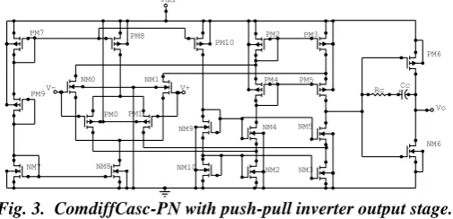
To implement a CCII+, the Complementary Differential Pair with NMOS Cascode Load (ComdiffCasc-PN) with
Push-Pull Inverter Output Stage [5] shown in Fig. 3, is the topology used as the op-amp block.
Fig. 3. ComdiffCasc-PN with push-pull inverter output stage.
The amp has rail-to-rail swing at both the input and output and has fewer stages than the other rail-to-rail op-amp configurations in [4], which makes it more stable. Also, its push-pull output stage further improves the differential gain and provides higher output voltage swing.
Setting all the transistor lengths (L) to 1.2µm, the initial op-amp transistor widths (W) may be solved using the current equation, given in Eq. 1, for a MOSFET in saturation. The reason for choosing the 1.2µm transistor length, instead of the minimum length of 0.25µm, is that short-channel effects are more significant at channel lengths less than 1um. Furthermore, submicron lengths for differential input pairs tend to introduce large offset voltage [6]. The tail current (Ibias) is set to be 20µm to minimize the total current and to meet the power consumption limits.
+Cc
Vo PM6
NM6
V- V+
Vdd
PM9
NM8
NM4
NM2 NM9
NM10 NM7
PM10
NM3 NM5 PM3 PM2
PM4 PM5 PM8
PM7
PM0 PM1 NM1 NM0
[Gomez* 6(2): February, 2019] ISSN 2349-4506
Impact Factor: 3.799
G
lobal
J
ournal of
E
ngineering
S
cience and
R
esearch
M
anagement
'
22
D GS T
k W
I V V
L
(1)
A width of 5µm/20µm is used for NMOS/PMOS transistors with Ibias/2 current. Plugging these values into the
schematic produced an op-amp differential voltage gain of less than 10,000, which is below the target gain of at least 1x10⁶. The transistor widths are then resized to increase the gain. A series of simulations aimed at
characterizing the op-amp were carried out. The effects of varying the width of each transistor on the op-amp parameters such as differential gain, common-mode gain, 3-dB bandwidth, unity-gain bandwidth and phase margin were studied and plotted. Finally, transistor sizes were assumed to be multiples of 6, to aid in the layout implementation. The compensation resistor (RC) and capacitor (CC) used were 10KΩ and 500fF, respectively.
Due to parasitics introduced by metal layers, the total output resistance in the layout simulations increased, as compared to schematic simulations – thus increasing the differential gain. However, slight mismatches in the layout and the lack of symmetry in routing also increased the common-mode gain, hence decreasing the CMRR.
Furthermore, these parasitics introduce more poles, thusdecreasing the bandwidth of the op-amp. It was also observed that the phase margin of the layout implementation is 20º lower than that of schematic simulations. As such, it is suggested that the phase margin be set at a relatively high value early in the schematic design stage to ensure stability in the layout stage.
Current conveyor block
The designed rail-to-rail op-amp is then connected to an output buffer stage before being paired with four types
of current mirrors, which are: Simple Current Mirror, Cascode Current Mirror, High-Swing Cascode Current
Mirror and Wilson Current Mirror. The requirements for the current mirrors to be used for the CCII+ are high output impedance, wide output voltage swing, small input bias voltage, and good high frequency response [7].
Even though the Op-Amp with Simple Current Mirror displayed the lowest output impedance among the four CCII+ implementations, it provided the highest current swing and had the least layout area and power consumption (having the least number of transistors) among all designs.
The positive input signal swing is determined by the state of transistor M1 while the negative input signal swing is determined by M2, as shown in Fig. 2. To have a functional output buffer stage, transistors M1 and M2 in Fig. 2 must remain saturated [7]. Therefore, the positive and negative input signal swing is restricted by Eq. 2-3.
1
IN DD T DSAT DSAT
V V V V V (2)
2
IN DSAT T DSAT
V V V V (3)
To minimize the voltage drop across the mirrors, the width of the transistors comprising the current mirrors is increased. This decreases the required VGS for saturation. Hence, decreasing the input bias voltage requirements
of the current mirrors increases the input swing at node X in Fig. 2. For uniformity and ease of layout, the widths of all the NMOS and PMOS transistors for the simple current mirrors are set to be 48µm and 192µm respectively.
CURRENT-MODE INSTRUMENTATION AMPLIFIERS
Initial simulations on the Improved 2-Current Conveyor (Improved 2-CC) in-amp, shown in Fig. 4, verified the
functionality of the Op-Amp with Simple Current Mirror. The in-amp produced a very high CMRR. However, it
[Gomez* 6(2): February, 2019] ISSN 2349-4506
Impact Factor: 3.799
G
lobal
J
ournal of
E
ngineering
S
cience and
R
esearch
M
anagement
Fig. 4. Improved 2-CC schematic design [8].
Stability was compromised due to the multiple stages employed in the CCII+ implementation. A series-RC compensation was placed between the buffer stage output and the current conveyor output node Z for all the CCII+ blocks used in all the in-amp circuits. The compensating resistor was set to 1KΩ while the compensating capacitor was limited to 2pF due to lay-out area considerations.
The 2-Current Conveyor (2-CC) is the most basic current-mode implementation of the in-amp. Any voltage difference applied between the in-amp inputs V+ and V- will also be reflected across RIN, forcing a current through
it.
Fig. 5. 2-CC schematic design [3].
By the operation of the CCII+, this same current will be conveyed and will then flow through RL. It can be derived
that the differential voltage gain of this topology is
( ) ( )
OUT L
VD
IN
V R
A
V V R
(4)
The resistors chosen for this circuit were 50KΩ for RL (as in the other topologies) and 500Ω for RIN to achieve a gain of 100. A large value of RL was needed to make the output voltage swing approach the supply rail despite the low current being passed at the output.
The configuration in Fig. 6 is an improvement to the 2-CC in-amp. As seen, an op-amp is added as an output stage to decrease the output impedance of the in-amp circuit. This op-amp, A3, is chosen to be tied at the output of the
conveyor A2 to produce a positive gain. As in the previous topology, the differential gain is given in Eq. 4.
The cascaded op-amp A3 is the same op-amp used in the CCII+ implementation, with the same sizing and biasing.
However, it was necessary to increase the compensation of the op-amp to make the 2-Current Conveyor with
Op-Amp at the Output (2-CC with Op-Op-Amp) stable. The op-amp’s CC was increased from 500fF to 2pF, while RC was
[Gomez* 6(2): February, 2019] ISSN 2349-4506
Impact Factor: 3.799
G
lobal
J
ournal of
E
ngineering
S
cience and
R
esearch
M
anagement
Fig. 6. 2-CC with op-amp at the output schematic design [4].
The positive terminal of A3 must bebiased to at least VDSAT, instead of just being grounded. This is to ensure that
the output current mirrors of the conveyor A2 have enough drain-source bias to maintain saturation, and thus
enables the conveyor A2 to properly mirror current iR1. In this design, a 1.25V-bias serves two purposes – aside from ensuring that conveyor A2 effectively mirrors the current iR1, it also raises the in-amp’s output reference
voltage to 1.25V, placing the output reference exactly between the rails. The 1.25V could be derived from the 2.5 VDD through voltage dividers.
The Improved 2-CC, shown in Fig. 4, is typified by a feedback loop from the unloaded output of A2 to the X
terminal of A1. Effectively, the voltages V- and V+ are imposed on the opposite ends of RIN and determines the value of the current i. This same current is forced to flow into the Z terminal of A2. Therefore, the total current
leaving the X and Z terminals of A1 is 2i. AVD can be calculated to be,
2
( ) ( )
OUT L
VD
IN
V R
A
V V R
(5)
The 3-Current Conveyor (3-CC) topology consists of three CCII+’s and two resistors, with current conveyors B and C cascaded. As seen in Fig. 7, the current entering RLis twice the current entering RIN, so AVD can be shown
in Eq. 5.
Fig. 7. 3-CC schematic design [9].
The CCII+ labeled as C, has VBIAS at its Y terminal instead of being directly grounded. Again, this is to ensure
that there is enough VDS at the output current mirrors of conveyor B. As done previously, VBIAS was set to 1.25V.
REPRESENTATION OF THE ECG SIGNAL
A representation of an ECG waveform using a piece-wise linear voltage source file is employed to verify the capability of the in-amps to accurately amplify ECG signals amidst common-mode noise. The model used in plotting the signal is adapted from related literature on biomedical signals. In addition, the simulated ECG signal was made to last for only 3 periods, so that simulations would not take much time.
[Gomez* 6(2): February, 2019] ISSN 2349-4506
Impact Factor: 3.799
G
lobal
J
ournal of
E
ngineering
S
cience and
R
esearch
M
anagement
RESULTS AND ANALYSIS
All the current-mode in-amp topologies achieved the fixed differential gain of 100, a superior CMRR of at least 150dB, and very high input impedance in the GΩ-range. However, the in-amps failed to provide a rail-to-rail input voltage signal swing because of the input signal constraints of the current conveyors. Hence, to allow the µV-range signal level of the ECG as input to the in-amps, the 1.25V DC input common-mode voltage was necessary.
No significant difference is observed between the 2-CC and the Improved 2-CC in-amps. Both topologies consume less power because they have fewer components compared to the other two topologies. The only difference between them is that the 2-CC has a greater tendency to suffer crosstalk due to the unused output of one of its conveyor blocks. The 3-CC in-amp, on the other hand, also produces the same performance despite the additional conveyor. Simulations have shown that aside from failing to produce an evident improvement in results, the third conveyor also degrades the bandwidth of the circuit and consumes more power.
The 2-CC with Op-Amp in-amp provides the smallest output impedance because of the addition of an op-amp as an output stage. Furthermore, this topology has an easily adjustable output reference voltage.
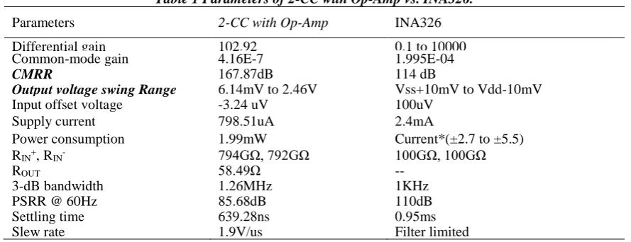
Shown in Table 1 is the comparison between the achieved parameters of the 2-CC with Op-Amp and the specifications of the INA326 [10], which is also a current-mode in-amp.
Table 1 Parameters of 2-CC with Op-Amp vs. INA326.
Parameters 2-CC with Op-Amp INA326
Differential gain 102.92 0.1 to 10000
Common-mode gain 4.16E-7 1.995E-04
CMRR 167.87dB 114 dB
Output voltage swing Range 6.14mV to 2.46V Vss+10mV to Vdd-10mV
Input offset voltage -3.24 uV 100uV
Supply current 798.51uA 2.4mA
Power consumption 1.99mW Current*(±2.7 to ±5.5)
RIN+, RIN- 794GΩ, 792GΩ 100GΩ, 100GΩ
ROUT 58.49Ω --
3-dB bandwidth 1.26MHz 1KHz
PSRR @ 60Hz 85.68dB 110dB
Settling time 639.28ns 0.95ms
Slew rate 1.9V/us Filter limited
Meanwhile, shown in Fig. 8 is the output plot obtained as the 2-CC with Op-Amp is applied with the simulated ECG signal and mode noise. Clearly, it can be seen that the in-amp has indeed rejected the common-mode signals incorporated in the simulated ECG signal.
[Gomez* 6(2): February, 2019] ISSN 2349-4506
Impact Factor: 3.799
G
lobal
J
ournal of
E
ngineering
S
cience and
R
esearch
M
anagement
CONCLUSION
In-amp designs should always take into account the trade-off between CMRR and stability. Simulations showed that a decrease in the common-mode gain increases the CMRR, thus compromising stability. Generally, cascading more stages to improve certain parameters, such as CMRR, worsens the stability of a system.
All the current-mode in-amp topologies achieve impressively high CMRR. Hence, any of the implemented current-mode circuits is an outstanding differential amplifier and thus, a potential ECG system block. However, the 2-CC with Op-Amp provides the lowest output impedance that is essential for connecting the in-amp into a larger system. It also has the advantage of being able to adjust its output reference voltage, allowing it to handle both negative and positive signals with respect to the reference voltage.
ACKNOWLEDGMENTS
The authors would like to express gratitude to Microelectronics and Microprocessors Laboratory of the University of the Philippines for the technical support during the course of the design and study. Author F. Gomez would like to extend appreciation to the STMicroelectronics Calamba NPI Team and the Management Team for the utmost support.
REFERENCES
1. J. G. Webster, Medical Instrumentation – Application and Design, 3rd ed., John Wiley and Sons, Inc.,
USA, 1998.
2. C. Kitchin, L. Counts, A Designer’s Guide to Instrumentation Amplifiers, 3rd ed. Analog Devices, Inc., 2006.
3. C. Toumazou, F. J. Lidgey, and C.A. Makris. “Current-mode instrumentation amplifier,” Short Run Press
Ltd., Exeter, 1993.
4. K. Koli and K. Halonen, “CMRR enhancement techniques for current-mode instrumentation amplifiers,”
IEEE Transactions on Circuits and Systems-I: Fundamental Theory and Applications, vol. 47, no. 5, May 2000.
5. M. Lorenzo and A. Manzano, “Design and implementation of CMOS rail-to-rail operational amplifiers,”
Department of Electrical and Electronics Engineering, University of the Philippines, October 2006.
6. P.R. Gray, P.J. Hurst, S.H. Lewis, and R.G. Meyer, Analysis and Design of Analog Integrated Circuits,
4th ed., John Wiley and Sons, Inc., USA, 2001.
7. A. Sedra and G. Roberts, “Current conveyor theory and practice,” Analogue IC Design: The
Current-mode Approach, Short Run Press Ltd., Exeter, 1993.
8. S. J. Azhari and H. Fazlalipoor, “A novel current mode instrumentation amplifier (CMIA) topology,”
IEEE Transactions on Instrumentation and Measurement, vol. 49, no. 6, December 2000.
9. A. A. Khan, M. A. Al-Turiagi and M. A. El-Ela, “An improved current-mode instrumentation amplifier
with bandwidth independent of Gain,” IEEE Transactions on Instrumentation and Measurement, vol. 44, no. 4, August 1995.
![Fig. 7. 3-CC schematic design [9].](https://thumb-us.123doks.com/thumbv2/123dok_us/8886477.1822801/5.595.217.384.509.608/fig-cc-schematic-design.webp)