Iranian Journal of Electrical & Electronic Engineering, Vol. 14, No. 2, June 2018 137
A Power Efficient Gain Enhancing Technique for Current
Mirror
T. Azadmousavi*, H. Faraji Baghtash*(C.A.) and E. Najafi Aghdam*
Abstract: This work introduces a new and simple method for adjusting the gain of current mirror. The major advantage of the proposed architecture is that, unlike the conventional variable gain current mirror, it does not need the change of the biasing current to adjust current gain. Therefore, the power dissipation remains constant in all of the gain settings. In addition, the proposed variable gain current mirror have linear-in-dB gain control characteristic, simple structure, and small occupied area. The gain of the current mirror can be simply varied from 1.3dB to 21dB while the 3-dB bandwidth of the circuit remains around 12.3MHz or 33.6MHz at operation frequency range of 1.9MHz-14.2MHz and 6.6MHz-40.2MHz respectively. The proposed circuit draws negligible power of 6.9µW from 1.8V supply voltage. The simulation results of designed variable gain current mirror in 0.18μm standard CMOS technology confirms the effectiveness of the proposed circuit.
Keywords: Variable Gain Current Mirror, Constant Power Consumption, Relocating Pole-Zero, Linear-in-dB.
1 Introduction1
N the recent years, using current mode signal processing has received significant attention due to the low-power operation, wide dynamic range, high frequency operation and simple structure [1-4]. One of the most important and widely used building blocks of current mode signal processing is variable gain current mirror (VGCM). For instance, it is commonly used in applications such as tunable filters and adjustable gain amplifiers. It also find its application in circuits designed for biomedical applications [5-8]. So far, various techniques introduced to control the current gain of current mirrors [9-11]. Currently, the research on tunable current mirrors are mainly focused on the reduction power consumption and increment of gain tuning range, and operating speed [12-15] .For instance, the power consumption in [12] has been decreased,
Iranian Journal of Electrical & Electronic Engineering, 2018. Paper first received 26 February 2017 and accepted 26 December 2017.
* The authors are with the Department of Electrical Engineering, Sahand University of Technology, Tabriz, Iran.
E-mails: [email protected], [email protected] and
Corresponding Author: H. Faraji Baghtash.
however, its tuning range and frequency bandwidth are very limited. On the other hand, [13] can deliver wide tuning range and frequency bandwidth, but it has a relatively high power consumption that is not suitable for ultra-low power applications. In all of these circuits, the operating current or voltage of circuit is varied to adjust the gain. As a result, the power consumption will be different at various gain settings. This, however, may not suitable for specific high performance applications that require ultra-low and constant power consumption. In this work, a new low power, linear-in-dB VGCM structure is introduced which delivers constant power consumption profile all-over the gain range. The proposed technique enables the structure to deliver some ever interesting features of low power consumption, wide programmable gain range, and acceptable frequency bandwidth. The paper is organized in four subsequent sections. The structure of proposed VGCM is described in Section 2. In the next section, simulation results using 0.18µm standard CMOS technology is presented. Finally, Section 4 concludes this work.
2 Proposed Circuit 2.1 Operational Principle
The conceptual schematic of the gain adjusting
I
Iranian Journal of Electrical & Electronic Engineering, Vol. 14, No. 2, June 2018 138 technique, is shown in Fig. 1. The main idea is to
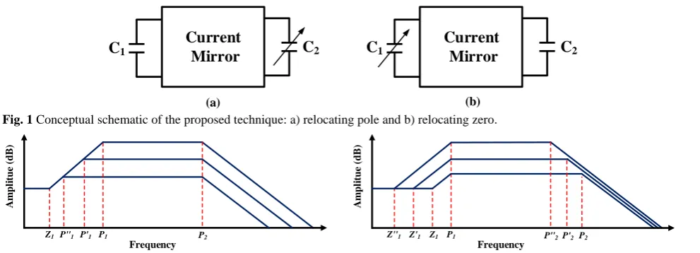
achieve the variable gain function through relocating the pole or zero of the circuit which originally proposed by authors in [16]. To better understand the operation of proposed technique, consider a current mirror with two dominate poles (P1, P2) and one zero (Z1), so that
Z1<P1<P2. Two distinct methods for tuning the gain of
current mirror can be introduced by relocating the pole or zero locations of current transfer function (see Fig. 2 and Fig. 3). The first method which we named it constant-zero variable gain current mirror (CZ-VGCM) is depicted in Fig. 2. As is depicted in this figure, in this method, our option to change the gain is to keep the values of Z1 and P2 constant, while relocating the P1 in frequency axis. This gives a constant 3-dB cutoff frequency at upper corner of frequency bandwidth that is very interesting in many automatic gain control (AGC) applications [17].
The second method to obtain variable gain function is to keep P1 constant while shifting both the P2and Z1 in the frequency axis. This method which we called it adjustable-zero variable gain current mirror (AZ-VGCM), in contrast with the first method, gives a frequency transfer function that has constant 3-dB cutoff frequency at lower corner while delivers different 3-dB cutoff frequency at higher corner of frequency bandwidth (see Fig. 3). The resulted VGCM, however finds its applications well in multi-standard transceiver structures [18]. Interestingly, in both cases of CZ-VGCM and AZ-CZ-VGCM, the current amplification is simply accomplished through varying the value of passive capacitors, which does not require extra power consumption. Thus, the resulted structure promised to be extremely low power. In other words, the proposed VGCM structure can interestingly works well with very low power consumption while, delivers high performance with acceptable gain control range. The transistor level realization of the proposed technique is described in the following section.
2.2Transistor level implementation of proposed VGCM
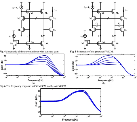
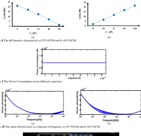
Figure 4 shows a current mirror with constant gain of I1/I2. In this circuit, the M1 and M8 form a source follower voltage buffer as well as M2 and M9 do. Through these two voltage followers, the gates of M3 and M4 follow the voltage of input node, constructing a current mirror circuit. There is an interesting feature with this structure, that is the capability of separately setting the gate voltage of M3 and M4 and consequently the mirroring ratio of current mirror by simply adjusting I1 and I2 (see Fig. 4). Transistors M5-M6 are cascade transistors which used to enhance the gain accuracy of current mirror. In order to add variable gain capability to the proposed CM, two adjustable capacitors are applied to the gate-drain nodes of M3 and M4. The final schematic of proposed VGCM is shown in Fig. 5. The proposed VGCM has two main poles and one zero. The capacitors C1 and C2 determine Z1, P2 and P1, respectively. By selecting the appropriate amount for C1
and C2, the zero can be located at lower frequencies
compared to the poles. Therefore, as described in previous section, the gain of the VGCM can be changed by relocating either zero and second pole or first pole.
3 Simulation Results
The proposed structure is simulated in TSMC 0.18µm standard CMOS technology. As the two versions of proposed VGCM (CZ-VGCM, AZ-VGCM) find very different applications, thus we examined the performance of each structure at different operating frequencies.
Therefore, in the circuit of CZ-VGCM, C1 is 29fF and
C2 varied from 6fF to 96fF and for AZ-VGCM, C2 is
29fF and C1 varied from 8fF to128fF. Fig. 6 shows the frequency response of the CZ-VGCM and AZ-VGCM at various gain settings. Fig. 6 (a) illustrates that the
Current
Mirror C2
Current Mirror
C1 C2
(a) (b)
C1
Fig. 1 Conceptual schematic of the proposed technique: a) relocating pole and b) relocating zero.
Z1 P"1 P'1 P1 P2
A
m
pl
itue
(
dB
)
Frequency
Z"1 Z'1 Z1 P1 P"2P'2 P2
A
m
pl
itue
(
dB
)
Frequency
Fig. 2 The frequency response of CZ-VGCM. Fig. 3 The frequency response of AZ-VGCM.
Iranian Journal of Electrical & Electronic Engineering, Vol. 14, No. 2, June 2018 139 current gain can be changed from 1.3dB to 21dB by
varying of C2, while its 3-dB bandwidth well-remains constant around 33.6MHz. Also, by changing of C1 the current gain of the AZ-VGCM ranges from 1.8dB to 21.6dB while its 3-dB bandwidth remains around 12.3MHz.
The Monte-Carlo simulation are done on the threshold voltage of the CZ-VGCM in the case of C1 is 6fF. The results are depicted in Fig. 7 and it shows that for the 15mv deviation of threshold voltage, the gain of the CZ-VGCM varied only 2.4dB. The current gain versus capacitor for CZ-VGCM and AZ-VGCM are plotted in Fig. 8, illustrating the linear-in-dB characteristic of the proposed structure.
The Power Consumption versus different capacitors of the proposed CZ-VGCM is shown in Fig. 9 and it validated the constant power consumption during the gain settings.
The input referred noise characteristic of the both VGCMs are shown in Fig.10, demonstrating very low
input referred noise. Fig.10 (a) represents that the input referred noise value well remains less than 1.1pA/√Hz all over the interested frequency bandwidth for CZ-VGCM. Also as shown in Fig.10 (b), the input referred noise value of the AZ-VGCM at its entire frequency bandwidth is evaluated to be less than 5.2pA/√Hz. The layout of the proposed VGCM is shown in Fig. 11 and the occupied area is 58 x 20 μm2.
Table 1 compares performance of the two versions of VCGM with Pre-Layout and Post-Layout simulation results. It demonstrates that AZ-VGCM is appropriate choice for applications which their operation frequency falls at 1.9MHz-14.2MHz range. On the other hand, for applications with operation frequency range from 6.6MHz to 40.2MHz, CZ-VGCM would be a good candidate. The transistors aspect ratios are given in Table 2. The performance compassion between the proposed VGCM (CZ-VGCM) and some other published works is reported in Table 3.
M2
M1
M3
M4
Ib2 + Iac
M5 M6
Iout
Ib1
M8
M9
I1 I2
M7
M2
M1
M3
M4
Ib2 + Iac
M5 M6
Iout
Ib1
M7 M8 M9
I1 I2
C1 C2
Fig. 4 Schematic of the current mirror with constant gain. Fig. 5 Schematic of the proposed VGCM.
104 105 106 107 108 109
-20 -10 0 10 20
Frequency(Hz)
G
a
in
(
d
B)
104 105 106 107 108 109
-20 -10 0 10 20
Frequency(Hz)
G
a
in
(
d
B)
(a) (b)
Fig. 6 The frequency response a) CZ-VGCM and b) AZ-VGCM.
104 105 106 107 108 109
-20 -10 0 10 20
Frequency(Hz)
G
a
in
(
d
B)
Fig. 7 The Monte-Carlo simulation results of 15mv deviation of threshold voltage.
Iranian Journal of Electrical & Electronic Engineering, Vol. 14, No. 2, June 2018 140
(a) (b)
Fig. 8 The dB-linearity characteristic a) CZ-VGCM and b) AZ-VGCM.
1 2 3 4 5 6 7 8 9
x 10-14 6
6.5 7 7.5
8x 10
-6
Capacitor (F)
P
o
w
e
r
Co
n
s
u
m
p
ti
o
n
(
W
)
Fig. 9 The Power Consumption versus different capacitors.
104 105 106 107 108 109
0 1 2 3 4
x 10-11
Frequency(Hz)
No
is
e
(
A/s
q
r(
Hz
))
1004 105 106 107 108 109
1 2 3 4
x 10-11
Frequency(Hz)
No
is
e
(
A/s
q
r(
Hz
))
(a) (b)
Fig. 10 The input referred noise as a function of frequency a) CZ-VGCM and b) AZ-VGCM.
Fig. 11 The layout of the proposed CZ and AZ VGCM.
Table 1 Comparison between two methods of tuning gain.
C1
(fF)
C2
(fF)
Gain range (dB)
Bandwidth 3-dB (MHz)
Frequency Operation (MHz)
Input Referred Noise (IRN)
pA/√ Hz
CZ-VGCMa 29 6-96 0-20.7 45 6.46-51.5 < 1
CZ-VGCMb 29 6-96 1.3-21 33.6 6.6-40.2 < 1.1
AZ-VGCMa 8-128 29 0-21 12 1.77-13.8 < 5
AZ-VGCMb 8-128 29 1.8-21.6 12.3 1.9-14.2 < 5.2
Iranian Journal of Electrical & Electronic Engineering, Vol. 14, No. 2, June 2018 141
Table 2 Transistors aspect ratios.
Transistor W/L (µm/µm) Transistor W/L (µm/µm)
M1,M2, M3,M4,M5,M7 0.4/0.18 M8 1/0.9
M6 5*×2/0.18 M9 1/0.18
* Number of Fingers
Table 3 Performance Comparison.
Works [12]* [13] [14] [15] This work
CMOS Process (µm) 0.35 0.18 0.5 0.18 0.18
Power Consumption (µW) 61 900 2.05 41.1 6.9
Supply Voltage (V) 1.5 1.5 ±1.2 1 1.8
3-dB Bandwidth (MHz) 1.708 100 0.189 93.7 33.6
Gain range (dB) -1.9 to 1.58 0 to 20 0 to 16 -4.3 to 14.9 1.3 to 21
IRN (pA/√Hz) - - - 4.33 < 1.1
*Measurement Results
4 Conclusion
In this paper a power efficient current gain adjustment technique is described. The operating principle of proposed structure is discussed. The proposed structure majorly enjoys from very low and constant power consumption all over the entire gain range. The proposed structure draws only 6.9µW from 1.8V power supply. Interestingly, the gain varies linear-in-dB with control signal and the structure presents constant bandwidth characteristic, both of which are very interesting parameters in variable gain structures. Simulation results in TSMC 0.18μm standard CMOS technology, confirm the proper function of the proposed design.
References
[1] J. K. Fidler, “Analogue IC design: The current-mode approach,” IEE Review, Vol. 37, No. 1, 33– 33, 1991.
[2] M. B. Ara and S. J. Azhari, “A low-voltage fully differential pure current mode current operational amplifier,” Circuits, Systems, and Signal
Processing,Vol. 35, No. 7, pp. 2626–2639, 2016.
[3] H. F. Baghtash, K. Monfaredi and A. Ayatollahi, “A novel±0.5 V, high current drive, and rail to rail current operational amplifier,” Analog Integrated
Circuits Signal Process., Vol. 70, No. 1, pp. 103–
112, 2012.
[4] A. Roohavar and S. J. Azhari, “An ultra high CMRR low voltage low power fully differential current operational amplifier (COA),” Iranian
Journal of Electrical and Electronic Engineering,
Vol. 11, No. 4, pp. 294–300, 2015.
[5] G. Tsirimokou, C. Psychalinos and A. S. Elwakil, “Digitally programmed fractional-order Chebyshev filters realizations using current-mirrors,” in IEEE International Symposium on Circuits and Systems
(ISCAS), pp. 2337–2340, 2015.
[6] M. Altun and H. Kuntman, “Design of a fully differential current mode operational amplifier with improved input–output impedances and its filter applications,” AEU-International Journal of
Electronics and Communications, Vol. 62, No. 3,
pp. 239–244, 2008.
[7] M. A. Youssef and A. M. Soliman, “A novel CMOS realization of the differential input balanced output current operational amplifier and its applications,” Analog Integrated Circuits and Signal
Processing, Vol. 44, No. 1, pp. 37–53, 2005.
[8] C. Laoudias and C. Psychalinos, “Applications of current mirrors in analog signal processing,” Physics Department, Electronics Laboratory, University of
Patras, Rio Patras, Greece, 2012.
[9] M. Tikyani and R. Pandey, “A new low-voltage current mirror circuit with enhanced bandwidth,” in
International Conference on Computational
Intelligence and Communication Networks (CICN),
pp. 42–46, 2011.
[10]M. Siripruchyanun, “A low-voltage, low-power current-mode automatic gain control (AGC) for battery-powered equipment,” in Third IEEE International Workshop on Electronic Design, Test
and Applications, 2006.
[11]A. Zeki and A. Toker, “Tunable linear CMOS current mirror,” Analog Integrated Circuits and
Signal Processing, Vol. 50, No. 3, pp. 261–269,
2007.
[12]C. Laoudias and C. Psychalinos, “Low-voltage CMOS adjustable current mirror,” Electronics
letters, Vol. 46, No. 2, pp. 124–126, 2010.
[13]B. Sedighi and M. S. Bakhtiar, “Variable gain current mirror for high-speed applications,” IEICE
Electronics Express, Vol. 4, No. 8, pp. 277–281,
2007.
Iranian Journal of Electrical & Electronic Engineering, Vol. 14, No. 2, June 2018 142 [14]M. Kumngern, F. Khateb and T. Kulej, “A digitally
programmable gain amplifier for ultra-low-power applications,” Analog Integrated Circuits and Signal
Processing, Vol. 85, No. 3, pp. 433–443, 2015.
[15]H. F. Baghtash, “Body controlled threshold voltage shifting variable gain current mirror,” Analog
Integrated Circuits and Signal Processing, Vol. 93,
No. 1, pp. 115–121, 2017.
[16]H. F. Baghtash and A. Ayatollahi, “A zero-pole reposition based, 0.95-mW, 68-dB, linear-in-dB, constant-bandwidth variable gain amplifier,”
Circuits, Systems, and Signal Processing, Vol. 33,
No. 5, pp. 1353–1368, 2014.
[17]E. Sobotta, R. Wolf, N. Joram and F. Ellinger, “RF variable gain amplifier with linear control and automatic matching in 28 nm CMOS,” in IEEE
International Conference on Microwaves,
Communications, Antennas and Electronic Systems
(COMCAS), pp. 1–5, 2015.
[18]K. Bao, X. Fan, L. Tang, Z. Hua and Z. Wang, “A programmable gain amplifier for mode multi-standard wireless receivers,” in 12th IEEE
International Conference on Solid-State and
Integrated Circuit Technology (ICSICT), pp. 1–3,
2014.
T. Azadmousavi was born in Urmia, Iran,
in 1989. She received her B.Sc. degree in Electronic Engineering from Urmia University, Urmia, Iran in 2011. Immediately after that, she started her M.Sc studies in Microelectronic Research Laboratory at Urmia University. She is currently Ph.D. student of Electronic Engineering at Sahand University of Technology. Her current research interests include, low power analog and digital integrated circuit, wireless RFIC design and frequency synthesizer.
H. Faraji Baghtash was born in
Miandoab, Iran, in 1985. He received the B.Sc. degree from Urmia University in 2007, and M.Sc. and Ph.D. degrees both from Iran University of Science and Technology (IUST), Tehran, Iran in 2009, and 2014 in respectively, all in electronics engineering. He was with IUST Electronic Research Center Group, from 2007 to 2010 as a Researcher, and Science and Research Branch, Islamic Azad University from 2011 to 2015, as a Fellow Lecturer. He joined Sahand University of Technology, Tabriz, Iran as an Assistant Professor in 2015. He is the author or coauthor of more than 30 national and international papers and also collaborated in several research projects and has a registered Iranian patent. Dr. Faraji Baghtash was selected as distinguished researcher of the IUST in 2011. His current research interests include current mode/voltage mode analog integrated circuit design, low voltage, low power circuit and systems, analog microelectronics and digital system design.
E. Najafi Aghdam was born in Zonouz,
Iran, in 1964. He received the B.E. degree from University of Sistan and Baluchestan, Zahedan, Iran, in 1990, and the M.Sc. degree from Amir-Kabir University of Technology, Tehran, Iran, in 1994, both in electronic engineering. In 1995, he joined the Department of Electric Engineering at Sahand University of Technology, Tabriz, Iran, as a Lecturer. In 2002, he started his Ph.D. program dealing with a high-performance bandpass Delta Sigma ADC. The research program is directed by Prof. P. Benabes at SUPELEC, France. Dr. Najafi Aghdam is now an Associate Professor at Sahand University of Technology. His current research interests include mixed mode electronic circuits, Delta Sigma Converters, RFIC design, Ultrasonic circuits and Electronic measurement.