PTMAC BASED ON RAZOR FOR ENERGY
REDUCTION IN DSP
Karthika.M
1, Gayathri.R
2, Mahalakshmi.K
31,2,3
ME VLSI Design, Thenni Kammavar Sangam College of Technology, (India)
ABSTRACT
The power optimization is achievable by dynamic voltage scaling using the fault tolerant technique by
improving the accuracy and/or timing performance against power. Energy improvements have a strong
dependency on the delay distribution of the circuit and the characteristics of the input signal. The fault tolerant
technique is implemented using Razor approach. The target power is also obtain by using the programmable
truncated multiplier (PTMAC) at the expense of degradation of the output signal to noise ratio. In the DSP
architecture the combination of PTMAC and fault tolerant technique are used to reduce the supply voltage
below the critical level. Truncated multiplication timing modulation properties are analysed and demonstrated
using Xilinx 12.1. Finally the two techniques are upgrade the energy saving beyond that expected in the DSP
architecture.
Keywords: DSP, Dynamic voltage scaling, Fault tolerant, PTMAC.
I. INTRODUCTION
Less power, area with high speed is the main theme in the VLSI based circuit design. Several techniques are
exists to reduce the energy consumption.
Voltage scaling is an effective method to minimize the energy consumption in CMOS integrated circuits. The
(DSP) digital signal processing system may possibly leverage unconventional voltage overscaling (VOS) to
decrease energy consumption while maintaining the satisfactory signal processing performance. Scaling the
supply voltage by a factor of K results in reduction in the dominating dynamic power consumption by a factor of
K2 and yields static power benefits [1].
In conventional practice, voltage scaling is lower bounded by Vdd-crit (critical supply voltage) under which
critical path delay equals the target clock period, voltage overscaling (VOS) (ie), overscaling the supply voltage
below Vdd-crit. Digital signal processing systems by applying unconventional voltage overscaling levels to further
improve the energy consumption levels while maintaining signal processing performance. The major
disadvantage of VOS is the latches or flip-flop on the critical path need a long execution time [3]-[5].
Fault tolerant is a property that enables a system operating properly in the event of failure. This technique can be
used to achieve power saving. It is dependent on process voltage temperature (PVT) and the circuit physical
design.
The ultimate aim is to design a multiplier of which possess less area usage and power that is possible with the
truncated multiplier [6]-[12]. The PTM mentions a full precision multiplier in which the elements of the partial
dynamic power consumption. The advantages are including dynamic power reduction and Flexibility in
accuracy selection.
The (Manuel de la Guia Solaz and Richard Conway) proposed a novel voltage management technique for
dynamic voltage scaled (DVS) processor, based on it situ error detection and correction, called Razor [4]. In this
technique, we use a delay-error tolerant flip-flop on the critical path to scale the supply voltage.
The PTMAC and the fault tolerant techniques are applied to a custom-designed fixed point multiply and
accumulate (MAC) in the DSP structure.
The work of this paper is organised as follows. A voltage scaling, fault tolerant and truncated multiplication
concept is deals in section II. Section III briefly explains the programmable truncated multiply and accumulate
(PTMAC) architecture. The combined process of the PTMAC and the fault tolerance using Razor technique are
analysed in section IV. Simulation result for power and energy reductions are reported in section V. Finally in
section VI conclusion and scope for future work on this paper are presented.
II. BACKGROUND
2.1
Voltage Scaling Beyond V
dd-critDynamic power consumption is the main component in many arithmetic unit circuits because of the high
toggling profile of such structures. The switching activity of the energy consumed by a digital gate is defined as
Pavg = α0→1CLV2 dd fclk in [13], where α0→1 is defined as the average number of times in each clock cycle
(at a frequency fclk) that a node with capacitance CL provide a power consuming transition. Reducing the
supply voltage by a factor of K results in a quadratic developement in the power consumption rate of CMOS
logic.
Scaling of Vdd results in timing penalties which increase as Vdd approaches the threshold voltages of the
devices [14]. relationship between the circuit delay (τd ) and the supply voltage Vdd is given by τd =
CLVdd/β(Vdd − Vt )α, where CL is the load capacitance, β ( gate transconductance), Vt (device threshold
voltage), and α ( velocity saturation index). We prefer to the critical supply voltage of a given architecture
Vdd−crit, as the minimum supply voltage where timing on the critical path is reached for any expected PVT
variations.
Scaling the supply voltage to Vdd = K ·Vdd−crit, where 0 < K < 1 is referred to as VOS; although this technique
results in further energy reduction almost proportional to K2, scaling Vdd below the critical supply voltage
results in critical timing failure for certain input combinations under certain PVT conditions. This is impractical
for use with designs that do not apply fault tolerant schemes.
2.2
Truncated Multiplication
Multipliers have become inevitable with the advancement of communication. In order to enable the
implementation of critical algorithms in DSP architectures the advancing VLSI play a significant role. A
truncated multiplier is an n × n multiplier with n bits output. In a truncated multiplier has n less significant bits
of the full-width product are discarded, some part of the partial products are removed and replaced by a suitable
compensation function, to trade- off accuracy with hardware cost. As a more columns are eliminated, the area
and power consumption of the arithmetic unit are significantly reduced, and in most cases the delay also
most commonly used in systems where least significant part of partial product can be skipped which leads to
low power consumption, area and timing. Here the partial product is split into two sections namely the (LSP)
and (MSP). The LSP is disabled or avoided to get the truncated output.
Truncated multiplications have been widely studied as a means of achieving both power and area improvements
in the field of arithmetic design, at the expense of signal degradation. As the truncated multipliers are smaller
than full-precision ones, they not only achieves improvements in power consumption and area, but result in
different timing distributions. The existence of synergic benefits derived from the combination of truncated
multiplication and VOS using a fault tolerance strategy is presented in brief where both techniques are applied
to a custom-designed fixed point multiply and accumulate (MAC) structure.
III. PTMAC-A FLEXIBLE LOW-POWER DSP WITH PTM
To develop the usage of PTM to general DSP architectures, the PTMAC was introduced and analyzed in [12]
and [19]. PTMAC, designed to exercise PTM in low-power biomedical applications with a need for modest
DSP such as ECG filtering or fall detection, to utilize in this brief as a platform to combine the benefits of
programmable truncation and fault tolerance.
Fig.1. PTMAC top level diagram.
The proposed DSP, as depicted in Fig. 1, includes a control unit operating in a five-stage pipeline, program and
memory blocks in a multibus Harvard configuration, some I/O connectivity and an arithmetic unit consisting of
a MAC structure with 16-bit PTM, 40-bit accumulator, and a 40-bit barrel shifter for scaling and rotating the
accumulated value.
The following gives the description of the important components of the DSP architecture.
3.1 Control unit
The control unit is simple 5 stage pipelines which fetch and decodes the instruction also controls the data flow,
of the internal block other than the arithmetic block. it allows the access of two data memory blocks and the
program memory block during the instruction read operation.
3.2 Custom Instruction Set
A custom instruction set was implement for the DSP so as to maximize the utilization of the ALU. This will
help in optimizing the power reductions Offer by the programmable truncated multiplier. All the Instructions
designed are 32 bits wide. The set of instructions include
3.2.1 Arithmetic and logic instructions
The arithmetic instruction includes addition operation, subtraction, multiplication with and without truncation
and also other operations such as multiply and accumulate operation, shifting,rotation of the accumulator output
also squaring of the accumulated value. All the arithmetic instructions utilize the arithmetic unit effectively. A
logic instruction performs all the logic operations.
3.2.2 Flow control instructions
The flow control instructions include instructions for jump operation, loop operations.
3.3.3 Dataflow instructions
It includes instruction for storing and loading data to and from different memory blocks.
3.3 Memory block
The memory block include two data memory blocks a program memory block. Each data memory has size 512
x 16 bits and the program memory size is 1024 x 32 bit, the data memory is store and load data,and program
memory is helpful to store the instructions. It is possible to access 3 memory blocks in a single clock cycle.
3.4 Arithmetic and logic unit
The ALU consists of the 16 bit programmable truncated multiplier,40 bit carry select adder,40 bit barrel
shifter/rotator and 40 bit accumulator. The ALU has a multiply and accumulate structure.A block diagram of the
Arithmetic Unit is displayed in Fig. The arithmetic unit consists of
3.4.1. PTM
The PTM is designed to operate as standard 16x16 bit multipliers that enable a programmable truncation. It
includes an additional control input for enabling and disabling the columns in the partial product matrix. Thus
the addition control input “truncation control” is used to control the truncation level of the multiplier.
3.4.2. Barrel shifter
A 40 bit barrel shifter/rotator is the main for shifting and rotating the accumulated output. The shifter process
left shifting, right shifting, left rotation and right rotation on the output of 40 bit accumulator.
3.4.3. Accumulator
A 40 -bit accumulator save the final result of the arithmetic operations. It is implemented from D flip-flops.
3.4.4. Carry select Adder
A 40- bit carry select adder is used for addition as well as subtraction operations. The carry select adder is a
IV. RAZOR IMPLEMENTATION
To goal the fault tolerance, the accumulator of the PTMAC was replaced by a fault tolerant version named
Razor Accumulator. The original flip-flops were substitute by a version of the Razor registers presented in [3].
In order to detect an error in the circuit level, each flip-flop is augmented by a shadow flip-flop. This flip-flop
was clocked by a delayed clock. If the combinational logic met the setup time of the main flip-flop, then the
main and delayed flop will latch the same value. In this case, the error signal remains low. If the main
flip-flop setup time is not met, then the main flip-flip-flop will latch a value that is different from the shadow flip-flip-flop.
The proposed augmented cells were design and stored as library cells for post synthesis insertion. Such a cell
obey the original implementation is Razor implementation, replacing the shadow latch within the Razor registers
with a shadow-flip-flop is used to avoid synthesis issues. The metastability detector required in Razor
implementations was modelled as the delay of an inverter .It added as a constraint to the hold time of the Razor
accumulator. In this method, all timing violations potentially causing metastability are then detected as timing
errors, providing a lower bound for the performance of Razor.The Razor technique was implemented using NI
multisim suite 12.0 software.
V. RESULTS
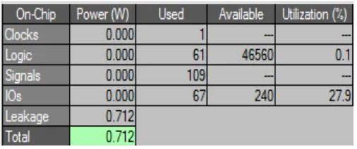
Fig .2. Power value of normal multiplier
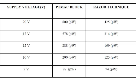
Table .1. Power of PT and Razor technique
VI. CONCLUSION
Fault tolerance was provided by implementing a conservative approach to the Razor I technique, and achieved
energy reductions over the original DSP implementation by enabling the reduction of Vdd beyond the original
critical supply level. Truncated multiplication was achieved by implementing a PTM, and resulted in energy
savings of the full design. Energy reductions achieved by fault tolerant techniques are limited by the overheads
required to provide error resilience and the amount of operations that need correction, therefore, they are highly
influenced by the delay distribution and maximum value of the system critical paths. The truncated
multiplication is achieved by interfacing them effectively with respect to the conditions after checking and
monitoring than the previous method. The use of Razor on a PTMAC structure has been tested at a post
synthesis simulation level to study the effect and interactions of both energy reducing techniques on a
previously tested DSP design. The timing and power effects of VOS with error correction and the application of
programmable truncated multiplication resulted in significant power reductions. The power consumption of
Razor on a PTMAC structure is also implemented in Multisim software. Thus, we have analyzed and compared
the performance results better than the conventional approach in terms of area, power and speed.
In the future work, delay- modulation properties of truncated multiplication and BIST using testable circuits
can be exploited to improve the energy.
REFERENCES
[1] Anantha P. Chandrakasan, Miodrag Potkonjak, Renu Mehra, Jan Rabaey, and Robert W. Brodersen
(1995) „Optimizing Power Using Transformations‟, IEEETrans. Comput.-Aided Design Integr. Circuits
[2] Byonghyo Shim, Srinivasa R. Sridhara, Naresh R. Shanbhag (2004) „Reliable Low-Power Digital Signal
Processing via Reduced Precision Redundancy‟,IEEETrans.Very Large Scale Integr. (VLSI) Syst., vol.
12, no. 5, pp. 497–510.
[3] D. Ernst, S. Das, S. Lee, D. Blaauw, T. Austin, T. Mudge (2004) „Razor: Circuit-level correction of
timing errors for low-power operation‟, IEEE Micro, vol. 24, no. 6, pp. 10–20.
[4] D. Ernst, N. S. Kim, S. Das, S. Pant, R. Rao, T. Pham (2003) „Razor: A low-power pipeline based on
circuit-level timing speculation‟ in Proc.36th Annu. IEEE/ACM Int. Symp.Microarch, pp. 7–18.
[5] Jiun-Ping Wang, Shiann-Rong Kuang, and Yuan-Chih Chuang (2006) „ Design of reconfigurable
low-power pipelined array multiplier‟ in Proc. Int.Conf.Commun.,Circuits Syst., vol. 4, pp. 2277–2281.
[6] Jin-Hao Tu and Lan-Da Van (2009) Power-efficient pipelined reconfigurable fixed-width Baugh-Wooley
multipliers,” IEEE Trans. Comput., vol. 58,no. 10, pp. 1346–1355
[7] Manuel de la Guia Solaz and Richard Conway (2012) „A flexible low power DSP with a programmable
truncated multiplier‟ IEEE Trans.Circuits Syst.I, Reg. Papers, vol. 59, no. 11, pp. 2555–2568.
[8] Matthew Fojtik, David Fick, Yejoong Kim, Nathaniel Pinckney, David Money Harris,David Blaauwand
Dennis Sylvester (2012) „Bubble Razor: An architecture-independent approach to timing-error detection and correction‟, in IEEE Int. Solid-State Circuits Conf.Dig.Tech.Papers,Feb. 2012, pp. 488–490.
[9] M. de la Guia Solaz and R. Conway (2010) „Comparative study on wordlength reduction and truncation
for low power multipliers‟, in Proc. 33rd Int. Conven., pp. 84–88.
[10] M. de la Guia Solaz, A. Bourke, R. Conway, J. Nelson, and G. OLaighin (2010) „Real-time low-energy
fall detection algorithm with a programmable truncated MAC‟, in Proc. IEEEAnnu. Int. Conf. Eng. Med.
Biol. Soc, pp. 2423–2426.
[11] Nicola Petra, Davide De Caro, Valeria Garofalo, Ettore Napoli, and Antonio G. M. Strollo (2010)
Truncated binary multipliers with variable correction and minimum mean square error IEEE
Trans.Circuits Syst.I, Reg. Papers, vol. 57, no. 6, pp. 1312–1325.
[12] Paul N. Whatmough, Shidhartha Das and David M. Bull (2013) „A low-power 1 GHz razor FIR
accelerator with time-borrow tracking pipeline and approximate error correction in 65 nm CMOS‟ in
IEEEInt. Solid-State Circuits Conf. Dig.Tech. Papers, pp. 428–429.
[13] Rajamohana Hegde, Naresh R. Shanbhag (2001) „Soft digital signal processing‟,IEEE Trans.Very Large
Scale Integr.(VLSI) Syst., vol. 9, no. 6, pp. 813–823.
[14] Shen-Fu Hsiao, Jun-Hong Zhang Jian, and Ming-Chih Chen (2013) „ Low-cost FIR filter designs based
on faithfully rounded truncated multiple constant multiplication/accumulation‟, IEEE Trans. Circuits Syst. II, Exp. Briefs, vol. 60, no. 5, pp. 287–291.
[15] Shiann-Rong Kuang and Jiun-Ping Wang (2010) „Design of power-efficient configurable booth
multiplier‟, IEEE Trans. Circuits Syst. I, Reg. Papers, vol. 57,no. 3, pp. 568–580.
[16] Shidhartha Das, Carlos Tokunaga, Sanjay Pant, Sanjay Pant, Sudherssen Kalaiselvan, Kevin Lai, David
[17] Sunder S . Kidambi, Fayez El-Guibaly, and Andreas Antoniou (1996) „Area-efficient multipliers for
digital signal processing applications‟, IEEE Trans. Circuits Syst. II, Analog Digit. Signal Process., vol.
43, no. 2, pp. 90–95.
[18] T. Sakurai and A. Newton (1990 ) „Alpha-power law MOSFET model and its applications to CMOS