INTRODUCTION
One of the most promising new developments in the field of solar research is thin film technologies. Due to using simpler deposition processes as compared with conventional techniques, thin film solar cells are much cheaper to manufacture. Polycrystalline CdTe thin films are
www.orientjchem.org
An International Open Free Access, Peer Reviewed Research Journal CODEN: OJCHEG 2015, Vol. 31, No. (2): Pg. 891-896
Optimization of High-Efficiency CdS/CdTe Thin Film
Solar Cell Using Step Doping Grading and Thickness
of the Absorption Layer
MASOUD SABAGHI
1, ABBAS MAJDABADI
1,
SAEID MARJANI
1,2* and SAEED KHOSROABADI
31Laser and Optics Research School, Nuclear Science and Technology Research Institute (NSTRI),
Tehran, Iran.
2Department of Electrical Engineering, Ferdowsi University of Mashhad, Mashhad, Iran. 3Department of Electrical Engineering, Imam Reza International University, Mashhad, Iran.
*Corresponding author E-mail: [email protected], [email protected] http://dx.doi.org/10.13005/ojc/310232
(Received: March 12, 2015; Accepted: April 04, 2015) ABSTRACT
In this paper, the influence of stepped doping of the absorber layer on performance of Cadmium Sulfide/Cadmium Telluride (CdS/CdTe) solar cell has been investigated. At first, the electrical characteristics of conventional CdS/CdTe solar cell is validated with fabricated CdS/CdTe solar cell. To improve the maximum efficiency of CdS/CdTe solar cell, the doping and thickness of the absorption layer are optimized. By step doping concentration within the absorber layer using buffer layer back contact and the increase in stepping gradient of the doping of CdTe layer, improved the conversion efficiency about 2.4% were obtained. The open-circuit voltage, short-circuit current density, fill factor and total area conversion efficiency of optimized solar cell structure are 952 mV, 25.97 mA/cm2,
78.5% and 18.7% under global AM 1.5 conditions, respectively.
Key words: Optimization, High efficiency, Step doping grading, Cadmium Sulfide/Cadmium Telluride (CdS/CdTe), Thin film solar cell.
normally used in a CdS/CdTe heterojunction configuration due to the high optical absorption coefficient. N. Amin et al proposed a ZnTe buffer layer as a back surface reflector in order to form an ohmic contact which improves the efficiency1. The
current densities2. The maximum efficiency for CdS/
CdTe solar cells were 28–30%3, 4 that have
increased by only 1.5% during the last 17 years [5-9]. Previous researchers reported 16% and 16.5% for maximum cell efficiency of CdS/CdTe solar cells10-13. The best CdS/CdTe solar cells
demonstrated the NREL show 17.3% and 18.7% for cell efficiency; and 12.8% and 13.1% for module efficiency at the lab condition14, 15. Consequently,
today major challenge is increasing the efficiency of CdTe thin film solar cells.
Structure, Model and its validation
When modeling thin film solar cells, it is essential to take into account the interaction of optical and electrical that occur during the solar cells operation. The fundamental equations are electrostatic potential and carrier densities, which link together. The primary equations are Poisson’s Equation, the continuity equations and transport equations that derived from Maxwell’s laws. Furthermore, The Concentration-Dependent Low Field Mobility model, Shockley-Read-Hall recombination model and SRH Concentration-Dependent Lifetime were used to model the doping-dependent low-field mobility, recombination model and carrier lifetimes, respectively. These equations are solved self-consistently with Silvaco ATLAS software16.
In this paper, we were used an experimentally-fabricated CdS/CdTe cell as a reference cell12, and our simulation results are very
close to the previous experimental results12.
Therefore, the results can be basically valid for an actual cell with the proposed configuration. Figure 1 shows the reference cell structure where glass is used as the substrate. Its layers were consisted of 200 nm indium-tin-oxide (ITO), 50nm CdS, 3.5µm CdTe. Table 1 listed all parameters used for simulation. It shows an open-circuit voltage of 840 mV, a short-circuit current density of 26.08 mA/cm2, a fill
factor of 0.731, and a conversion efficiency of 16.0% under AM 1.5 conditions. Table 2 compares the experimental results of JSC, VOC, fill factor, and cell efficiency with the simulated ones. As seen, the simulated results quite close to the actual experimental data.
RESULTS AND DISCUSSION
The step doping profile increases the efficiency of the CdS/CdTe cell due to formation of built-in electrical field that assists carrier migration and reduces the charge storage time and series resistance of the absorbing layer. The step doping profile can be form with divination of the absorption layer into two layers with different doping levels. The thickness and doping coefficients of the top
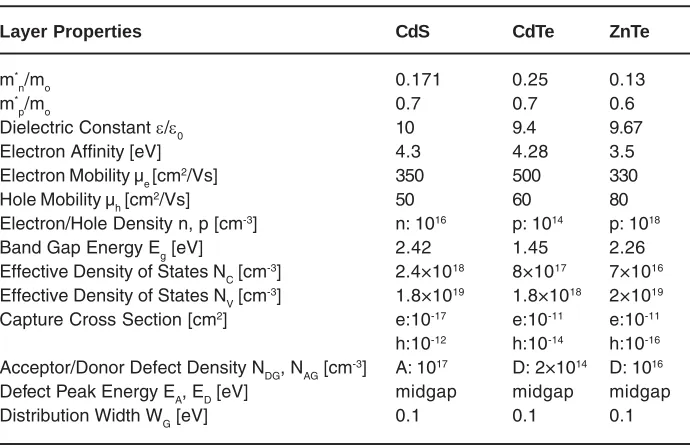
Table 1: Best Physical Parameters1
Layer Properties CdS CdTe ZnTe
m*
n/mo 0.171 0.25 0.13
m*
p/mo 0.7 0.7 0.6
Dielectric Constant /0 10 9.4 9.67
Electron Affinity [eV] 4.3 4.28 3.5
Electron Mobility µe [cm2/Vs] 350 500 330
Hole Mobility µh [cm2/Vs] 50 60 80
Electron/Hole Density n, p [cm-3] n: 1016 p: 1014 p: 1018
Band Gap Energy Eg [eV] 2.42 1.45 2.26
Effective Density of States NC [cm-3] 2.4×10¹⁸ 8×10¹⁷ 7×10¹⁶
Effective Density of States NV [cm-3] 1.8×10¹⁹ 1.8×10¹⁸ 2×10¹⁹
Capture Cross Section [cm2] e:10-17 e:10-11 e:10-11
h:10-12 h:10-14 h:10-16
Acceptor/Donor Defect Density NDG, NAG [cm-3] A: 1017 D: 2×10¹⁴ D: 1016
Defect Peak Energy EA, ED [eV] midgap midgap midgap
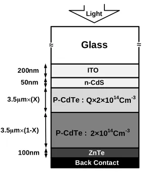
layer of CdTe layer have defined with X and Q parameters, respectively. The thickness of the top and the bottom layer were set as 3.5×X (µm) and 3.5× (1-X) (µm), respectively. The top and bottom layer doping concentrations were set as Q×2×1014cm-3 and fixed 2×1014 cm-3 value,
respectively. Figure 2 shows this cell configuration schematically.
In addition to optimizing the doping levels, various structures by using step doping grading of the CdTe layer were also investigated in order to achieve best device performance. Therefore, the both doping and thickness of the top CdTe layer were optimized. An increase in the step doping gradient causes the decrease of charge storage time considerably. As compared with the uniformly doped reference cell, all step graded doping structures exhibited higher efficiency.
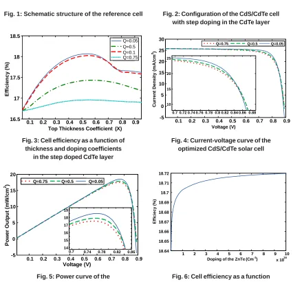
Figure 3 shows the effect of varying X and Q in cell efficiency of the new structure. As can be seen, the efficiency is the maximum (18.07%) for X=0.64 and Q=0.05. The fill factor of 0.818 obtained for the best step graded doping structure.
Figures 4 and 5 show characteristics of the proposed structure for various values of Q (Q=0.75, 0.5 and 0.05). As seen these figures, the efficiency is maximum at the value of Q=0.05.
One of the major challenges associated for the fabrication of efficient and long-term stable CdS/CdTe solar cell is the formation of a stable, low resistance, non-rectifying contact to p-CdTe thin film. A high work function metal is required to make good ohmic contact to CdTe since CdTe is a p-type semiconductor with high electron affinity while most metals do not have sufficiently high work
functions. Therefore, Schottky-barrier contacts to p-CdTe absorber layers are normally used. The presence of a back contact barrier can significantly affect the current–voltage characteristics of a CdTe cell, primarily by impeding hole transport. Furthermore, it causes the current-limiting effect referred to as “rollover” causing form Schottky, or blocking barriers. The use of heavily doping extra buffer layer between the CdTe and metal back contact interface is a typical approach to overcome this problem. Moreover, the buffer layers are essential for achieving highly efficient solar cells. Figure 6 shows the resulted structure with the optimized CdTe thickness.
In order to form an ohmic contact, the 100 nm of Zinc Telluride (ZnTe) with a direct band gap of 2.28 eV was used as a back contact buffer layer in this work. Since ZnTe can dope highly p-type, the efficiency of our structure as a function of its doping was plotted. Figure 7 shows impact of increasing in impurity of the ZnTe layer on the J-V characteristics. As seen, due to increasing the open-circuit voltage, the efficiency increase.
Another attractive quality of the ZnTe is the low valence band discontinuity with CdTe. Table 2: Comparison between the characteristics
of the reference cell and the simulated cell
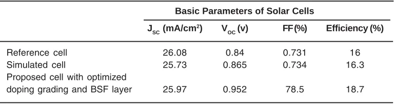
Parameters Reference Simulated
cell cell
VOC (mV) 840 865
JSC (mA/cm2) 26.08 25.73
Fill factor 0.731 0.734
Efficiency (%) 16 16.3
Table 3: Output Parameters of Different Cells Basic Parameters of Solar Cells JSC (mA/cm2) V
OC (v) FF (%) Efficiency (%)
Reference cell 26.08 0.84 0.731 16
Simulated cell 25.73 0.865 0.734 16.3
Proposed cell with optimized
n-CdS ZnTe Back Contact Light ITO
≈
≈
Glass
50nm 200nm3.5µm×(1-X)
P-CdTe :
3.5µm×(X) Q×2×10¹⁴Cm-3
P-CdTe : 2×10¹⁴Cm-3
E ffi cien cy ( % )
0.1 0.2 0.3 0.4 0.5 0.6 0.7 0.8 0.9
16.5 17 17.5 18 18.5 Q=0.05 Q=0.5 Q=0.1 Q=0.75
Top Thickness Coefficient (X)
1 2 3 4 5 6 7 8 9 10 x 1016 18.64 18.65 18.66 18.67 18.68 18.69 18.7 18.71 18.72
Doping of the ZnTe (Cm-3 ) E ff iciecy ( % ) n-CdS ZnTe Back Contact Light ITO
≈
≈
≈
≈
Glass
50nm 200nm3.5µm P-CdTe : 2×10¹⁴
Cm-3
Fig. 1: Schematic structure of the reference cell Fig. 2: Configuration of the CdS/CdTe cell with step doping in the CdTe layer
Fig. 3: Cell efficiency as a function of thickness and doping coefficients
in the step doped CdTe layer
Fig. 6: Cell efficiency as a function of doping in the ZnTe layer
0.1 0.2 0.3 0.4 0.5 0.6 0.7 0.8 0.9
-5 0 5 10 15 20 25 30
Q=0.75 Q=0.5 Q=0.05
0.7 0.72 0.74 0.76 0.78 0.8 0.82 0.84 0.86 0.88 10 15 20 25 Voltage (V) C u rr en t D en s it y (m A/ c m 2)
Fig. 4: Current-voltage curve of the optimized CdS/CdTe solar cell
0.1 0.2 0.3 0.4 0.5 0.6 0.7 0.8 0.9
-5 0 5 10 15 20
0.7 0.74 0.78 0.82 0.86 14 15 16 17 18 19
Q=0.75 Q=0.5 Q=0.05
Voltage (V) Pow e r Ou tp u t (m W /c m 2 )
Therefore, it provides no drawback to the flow of holes towards the contact. The efficiency of new structure was 18.7%. Figure 8 shows calculated J-V data for following three structures:
A) Uniform doping of CdTe layer B) Stepped doping of the CdTe layer
C) Stepped doping of the CdTe layer with the ZnTe buffer layer.
The results show that the structure C has the best efficiency. The open-circuit voltage, short-circuit current, fill factor and conversion efficiency for reference cell, simulated cell and proposed cell with optimized doping grading and BSF layer are given in Table 3.
CONCLUSIONS
In this paper, we evaluated several step doping profiles in the absorber layer of CdS/CdTe cells. The conversion efficiency of 18.7% was obtained by optimization of the homo-junction location, doping concentrations and using ZnTe buffer layer that showed a noticeable improvement over the 16.3% efficiency of the reference cell with uniform doping profile of absorber layer. In addition, the modifications can be easily implemented during the fabrication process. The results show the conventional structure with ZnTe as a buffer back contact is the best structure. The open-circuit voltage, short-circuit current density, fill factor and total area conversion efficiency of the optimized solar cell structure are 952 mV, 25.97 mA/cm2, 78.5% and
18.7%, respectively under global AM 1.5 conditions.
REFERENCES
1. Amin, N.; Sopianb, K.; Konagai, M.; Solar Energy Materials and Solar Cells 2007, 91, 1202–1208
2. Kr ishnakumar, L.; Han, J.; Klein, A.; Jaegermann, W.; Thin Solid Films 2011, 519, 7138-7141
3. Meyers, P.V.; Albright, S.P.; Progress in Photovoltaics: Research and Applications
2000, 161-168
4. Bonnet, D.; CdTe thin-film PV modules, In Practical Handbook of Photovoltaic: Fundamentals and Applications, Elsevier,
0.1 0.2 0.3 0.4 0.5 0.6 0.7 0.8 0.9 -5
0 5 10 15 20 25 30
Volatge (V)
C
u
rr
en
t D
e
n
s
it
y
(mA
/cm
2) Structure A
Structure B Structure C
-5 0 5 10 15 20 25 30
P
o
we
r Ou
tp
u
t (
m
A
/c
m
2
)
n-CdS
ZnTeZnTe
Light
ITO
≈
≈ Glass
50nm 200nm
3.5µm×(1-X)
P-CdTe :
3.5µm×(X) Q×2×10¹⁴Cm-3
P-CdTe : 2×10¹⁴
Cm-3
ZnTe Back Contact
100nm
Fig. 7: Cell structure with optimized absorption layer and BSF layer
Fig. 8: Current-voltage curve of the optimized CdS/CdTe solar cell for three structures. A)
Uniform doping of CdTe layer. B) Stepped doping of the CdTe layer. C) Stepped doping of
Oxford, (2003)
5. M.A. Green, K. Emery, Y. Hishikawa, W. Warta, E.D. Dunlop, Progress in Photovoltaics: Research and Applications 2011, 19, 84-92 6. Kosyachenko, L.A.; Savchuk, A.I.; Grushko, E.V.; Thin Solid Films 2009, 517, 2386–2391 7. Britt, J.; Ferekides, C.; Applied Physics Letters
1993, 62, 2851-2852
8. Pena, J. L.; Ares, O.; Rejon, V.; Rios-Flores, A.; Camacho, J. M.; Romeo, N.; Bosio, A.; Thin Solid Films 2011, 520, 680-683
9. Colegrove, E.; Banai, R.; Blissett, C.; Buurma, C.; Ellsworth, J.; Morley, M.; Barnes, S.; Gilmore, C.; Bergeson, J. D.; Dhere, R.; Scott, M.; Gessert, T.; Sivananthan, S.; Journal of Electronic Materials 2012, 41, 2833-2837 10. Razykov, T.M.; Ferekides, C.S.; Morel, D.;
Stefanakos, E.; Ullal, H.S.; Upadhyaya, H.M.;
Solar Energy 2011, 85, 1580–1608 11. Rios-Flores, A.; Ares, O.; Camacho, J. M.;
Rejon, V.; Pena, J.L.; Solar Energy 2012, 86, 780–785
12. Aramoto, T.; Ohyama, H.; Kumazawa, S.;
Japanese Journal of Applied Physics 1997,
36, 6304-6305
13. Wu, X.; Keane, J.C.; Dhere, R.G.; DeHart, C.; Albin, D.S.; Duda, A.; Gessert, T.A.; Asher, S.; Levi, D.H.; Sheldon, P.; in Proc. 17th Conf. IEEE
European Photovoltaic Solar Energy, 2001, Munich, Germany, 995–1000.
14. First Solar, Press Release: First Solar Sets World Record for CdTe Solar PV Efficiency, 2011, http://investor.firstsolar.com/ releasedetail.com.
15. First Solar Inc., 2013, http://www.firstsolar. com/en/Innovation/Advanced-Thin-Film-Modules.