Design of Low Voltage CMOS OTA Using Bulk - Driven Technique
Siddharth Bhat SRM University India
Shubham Choudhary SRM University India
[email protected] Jayakumar Selvakumar
SRM University India
ABSTRACT: In this paper, we have a designed a low voltage CMOS operational transconductance amplifier (OTA) for high
speed transmission with an operating voltage 0.5 V. The transistors are operating in the sub-threshold region with source degeneration for transconducatnce improvement. The OTA achieves a DC gain (Ao) of 26 dB, a gain-bandwidth product (GBW) of 750 MHz, slew rate (SR) of of 3.7 V μ s, a phase margin (PM) of 98º, DC offset of 2.2 mV and a power dissipation of 250 μ W under no load condition The proposed OTA is simulated in 90-nm CMOS technology using Cadence EDA software.
Keywords: Operational transconductance amplifier; low voltage; sub-threshold; source degeneration.
Received: 17 April 2016, Revised 26 April 2016, Accepted 12 May 2016
1. Introduction
inversion) region. There are various approaches like floating gate approach, selfcascode structures and bulk-driven transistors. The utilization of bulk-driven differential pair might beat a few requirements forced by supply voltages in situations where its power supply is of the same request as the threshold voltages [2]. Recent publications which are using this technique has provided dependable low voltage and low power amplifiers [1][3]-[7]. Although one of the huge difficulties for the bulk-driven technique is the reduction in gmb / gm ratio in the CMOS technologies there are some drawbacks of the bulk-driven technique like the value of gmb will be 5-8 times smaller than the value of gm and very large parasitic capacitance on the bulk and high input referred noise. Therefore, we represent a differential pair operating in sub-threshold region using bulkdriven technique as one possible solution to contend with the gmb= gm ratio reduction by upgrading the transconductance and enhancing the unity gain frequency (fT) as well as the open loop gain without increasing the power consumption. The principle of the bulk-driven technique is that the input signal is given at the bulk terminal which is less than the threshold voltage and a voltage is being set on the gate terminal so as to form a channel. The thickness of the depletion zone i.e. the conduction channel is affected by the bulk voltage. A bulkdriven symmetrical OTA operating in weak inversion can result in both reduced power consumption and high linearity. For a standard CMOS technology only PMOS can be bulk driven due to the fabrication process. The utilization of the bulk-driven technique makes it conceivable to design lowvoltage OpAmps with very large value of input CMRR and low power dissipation on the CMOS technologies.
In this paper we have used conventional transistors as compared to the halo implanted transistors [1]. Finally , a low voltage OTA using bulk driven technique is simulated with improved various parameters such as slew rate, the effective transconductance, input referred noise, phase margin, as well as improvement in other OpAmp performance parameters.
In section 2, a brief on the basic theory of the bulk driven technique and weak inversion operation is mentioned. In section 3 details of the proposed OTA are described and simulation results are shown and discussed in section 4 of the proposed OTA. In section V, an application approach is simulated using the proposed OTA. Section 6 concludes the paper.
2. Basic Theory of The Bulk - Driven Technique And Weak Inversion Operation
Bulk-driven MOSFET was first adopted in [8]. While designing an OTA while adopting the bulk-driven technique the most significant stage is the input stage. In this technique, the gate terminal is tied to a fixed bias voltage and the input is given into the bulk terminal as shown in fig. 1. With the zerobias voltage on the bulk terminal the transistors are in the subthreshold region. The two fundamental favorable circumstances of utilizing the bulk-driven system are that the bulk- driven differential sets in an OpAmp and incredibly enhances the transconductance and the threshold voltage of the transistor vanishes and both negative and positive bias voltages (VBS) are conceivable. For a standard n-well CMOS process, only PMOS devices can be used as a bulk-driven transistor because of the twin tub fabrication process. Whereas there are a couple of downsides to the bulk-driven technique when contrasted with the gate driven method, for example, little transconductance due to the less input capacitance of the depletion layer and larger parasitic capacitance to the mass which diminishes the fT. Due to the smaller transconductane
the device will have high input referred noise. By setting the input signals on the substrate instead of gate terminals the input differential pair will results in large input CMRR of the OpAmp. The enhancement in the transconductance is determined by the positive feedback.
The drain current IDS of the MOS transistor operating in weak inversion is based on a channel diffusion current that can be expressed [2] as
IDS a exp (qVGS / nkT) exp[ q(n-1) VBS / nkT]
Where n is the slope factor in sub-threshold, which can be defined as 1+gmb /gm it is in fact not a consistent variable but rather a component of the process parameters and substrate biasing [9]. The effect of VBS on the current IDS is lower by the component (n-1) contrasted with the VGS. This gives fundamental further point in expected transconductance in the bulk-driven circuits. The transistor will be operating in weak inversion when VDS > 3kT/q [9]. This paper presents simulated results only ofan improvement in the transconductance for input bulk-driven differential pair. The transconductance of the differential pair is defined as
Gm = dIo / dVin
(1)
Figure 1. Bulk-driven nMOS
Where Io is the output current and V in is the input voltage. As the CMOS scaling is done, the ratio of gmb and gm decreases, however the improvement element (n+1)/(n-1) ratio increments demonstrating the overall transconductance will increment with scaling.
3. Proposed - Bulk Driven Ota Circuit
Fig. 2 shows the circuit diagram of the proposed bulk-driven OTA circuit. The proposed OTA consists of two differential pairs. The input signal is given on the bulk terminal of the ptype transistors in the first differential pair. It consists of four p-type transistors. The four transistors are represented as M1a , M1b , M2a ,M2b. The transistors M1a and M2a are identical, whereas the M1b and M2b are also identical. The drains of the M1b and M2b are connected to the other differential pair. The reference current (IREF) is given as 500 μA. Moreover, the slew rate to the amplifier is determined by the reference current. The main objective of the proposed OTA is that the all the transistors should work in sub-threshold region or the weak inversion region. The circuit has a operating voltage of 0.4 V. The PMOS transistors are used as active load of differential pair is given by two identical transistors M3 and M4 , they are split into four transistors, the active loads M3a and M4a and the common gate (CG) amplifiers M3b and M4b.
There is an expansion in the DC shift for higher swing and high output impedance. The last stage comprises of transistor M6 as the input transistor and transistor M7 as its active load. The compensation circuit consists of a capacitor of 100fF. The capacitor Cc is placed inside the output stage to establish the dominant pole associated. The location of the dominant pole is pushed to a lesser value due to Miller effect of the capacitor Cc. It is basically an on-chip amplifier. The Bandwidth of the proposed OTA is significantly very large, which therefore leads to higher gain bandwidth product (GBW). The frequency should be high for the design of OTA such that the total phase margin of more than 60 f can be obtained.
4. Simulation Results
Fig. 3 represents the transient response of the proposed OTA with the operating frequency of 100 Hz, 10-mVpp input to only the inverting input terminal. The rise time is about 10 ns. Fig. 4 shows the simulated bode diagrams for the proposed bulk-driven OTA. The output impendence do not depend on the bulk-driven differential pair and change in open loop gain. The unity gain frequency is dependent to the change in transconductance. The gain of the proposed bulk driven OTA is less which is a disadvantage of the circuit. But there are other parameters which are having good value. The reference current is 500 μ A with the power supply of 0.4 V, allowing all the transistors operating in weak inversion. All nMOS and pMOS threshold voltages are 80 mV and 140 mV respectively.
Figure 4. Simulated bode diagrams for the proposed bulk-driven OTA
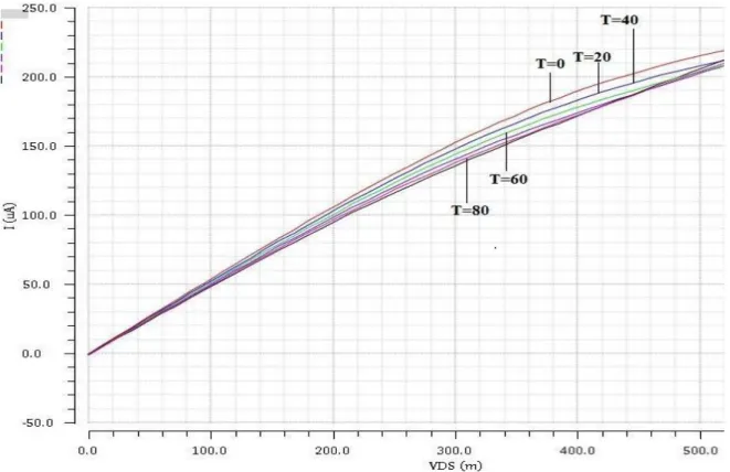
Fig. 5 demonstrates the change on the output current with change in the temperature. The simulated results verify that there is an increase in the output current as the temperature is increasing. At T=0
°
f the output current increases and becomes constant when the input voltage is 0.5 V. At T=20°
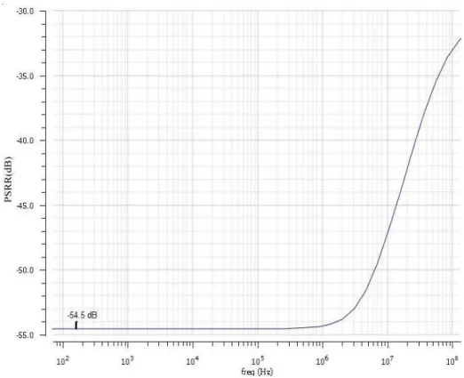
f the output current increases and decreases when voltage is 0.5 V. Current variation is shown with change in temperature. The PSRR performance is also simulated when the conditions are VDD = 0.5 V and no load condition. The simulated result is shown in Fig. 6. The proposed OTA with bulk driven technique achieves a PSRR of 54.5 dB at low frequencies whereas the roll-off frequency is ∼100 Hz.Table 1. lists the performance comparisons between the proposed OTA and several previous papers. The analysis is done by using Cadence tool. The PSRR of the proposed OTA is -54.5 dB at 100 Hz. The value of PSRR reduces at high frequencies. The circuit is having high PSRR due to the output capacitance. The value of the PSRR is directly proportional to the output capacitance. Due to the value of biasing current, high slew rate of the proposed bulk-driven OTA is achieved. The equation (3) shows the pole frequency expression fnd of the bulk-driven proposed OTA can be given by
fn d= gm6 /2πCL
(3)
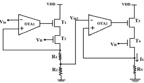
5. V-I Convertor By Using Bulk - Driven Ota CircuitFig. 7 shows the most simple configuration of a I converter. The design is made out of a buffered voltage divider before the V-I converter. Attenuation of the input voltage is done by a rail to rail input voltage divider before the V-V-I converter. The V- V-I converter is thereby essentially composed of two V-I converters in cascade. The functioning involves the input voltage Vin being buffered to the OTA voltage follower with the input-output voltage being rail to rail. A modular circuit can be set only with cascode configuration so that in the second phase the cascode transistors can enhance the current being copied and increaseoutput resistance. The voltage divider formed of resistors attenuates the voltage being buffered given by the formula.
α = R2 / (R1+R2)
Performance [1] [2] [3] [6] Parameters
Technology 350 nm 130 nm 350 nm 350 nm 90 nm
Power supply 0.5V 0.25V 0.5V 0.5V 0.5V
Transconductance n.a 9.3 nS n.a n.a 440 S
Maximum input current < 10 nA < 3 nA 2.15 nA < 10 nA < 1 nA
DC gain 88 dB 60 dB 76 dB 64 dB 26 dB
Phase margin 66.1° 52.5° n.a 44° 98°
Slew rate 2.53 V/s 0.64 V/ms 2.74 V/s 0.7 V/s 3.70 V/s
DC offset voltage 8.4 mV 2.8 mV 1.3 mV 10 mV 2.2 mV
Input referred thermal noise 0.2 mV/HZ 3.3 mV/HZ 0.9mV/HZ 165nVHZ 180 nV/HZ
PSRR 40 dB n.a n.a n.a 54.5 dB
GBW n.a n.a n.a n.a 750 MHz
Power consumption 197 W 18 nW 358W 130 W 250W
This work2015
Table 1. Proposed Ota Performance Comparison
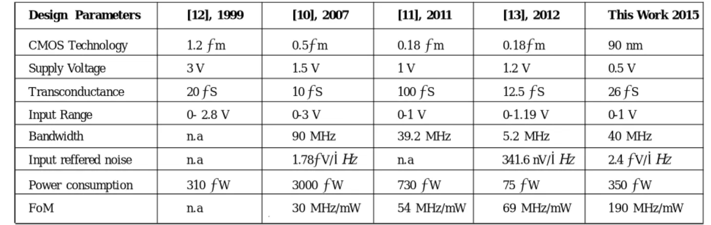
De sig n Paramete rs [12], 1999 [10], 2007 [11], 2011 [13], 2012 This Work 2015
CMOS Technology 1.2 m 0.5m 0.18 m 0.18m 90 nm
Supply Voltage 3 V 1.5 V 1 V 1.2 V 0.5 V
Tra nsconducta nce 20 S 10 S 100 S 12.5 S 26 S
Input Range 0- 2.8 V 0-3 V 0-1 V 0-1.19 V 0-1 V
Bandwidth n.a 90 MHz 39.2 MHz 5.2 MHz 40 MHz
Input reffered noise n.a 1.78V/HZ n.a 341.6 nV/HZ 2.4 V/HZ
Power consumption 310 W 3000 W 730 W 75 W 350 W
FoM n.a 30 MHz/mW 54 MHz/mW 69 MHz/mW 190 MHz/mW
Table 2. V-I Convertors Performances
The voltage is buffered to
V
A=V
in2= Vout1= Vin.Then, the generated current I1=Vin / Rs.
The FoM from [13] can be expressed as
FoM = [Vin / VDD ] * BW / power
Publications published recently which are linear rail-to-rail V-I converters derived by implementing passive resistors at the input terminals [10][11].
Figure 7. V-I convertor using bulk-driven OTA
6. Conclusion
In this paper a low voltage OTA using bulk-driven input differential pair is presented. The circuit is simulated in 90-nm standard CMOS process using Cadence EDA software. The methodology utilized a source degeneration of a positive feedback in a differential pair to enhance the transconductance and the slew rate. The change in the transconductance, the execution parameters of the OpAmp, for example, slew rate, UGBW, GBW are all upgraded. The GBW of the OpAmp is 750 MHz and the slew rate is 3.7 V/μ sec while achieving a PSR of ∼55 dB with a 0–100-kHz frequency range. The power consumption is 250 μW with a supply voltage of 0.5 V making this OpAmp very useful in high speed transmission and biomedical applications.
References
[1] Zuo, L., Islam, S.K (2013). Low-voltage bulkdriven operational amplifier with improved transconductance, IEEE Trans. Circuits Syst. I, Reg. Papers, 60 (8) 2084–2091, Aug. 2013.
[2] Ferreira, L. S. Sonkusale, R (2014). A 60-dB Gain OTA operating at 0.25 V power supply in 130 nm digital CMOS process, IEEE Trans. Circuits Syst. I, Reg. Papers,. 61 (6) June 2014.
[3] Carrillo, J. M., Torelli, G., Perez-Aloe, R., Duque-Carrillo, J.F (2007). 1-V rail-to-rail CMOS opamp with improved bulk-driven input stage, IEEE J. Solid-State Circuits, v.42, p. 508.
[4] Ferreira, L. H. C., Pimenta, T. C., Moreno, R. L. (2007). An ultra-low-voltage ultra-low-power CMOS miller OTA with rail-to-rail input/output swing, IEEE Trans. Circuits Syst. II, Exp. Briefs, 54 (10) 843–847, Oct. 2007.
[5] Cotrim, E.D., Ferreira, L. H. C.(2012). An ultralow- power CMOS symmetrical OTA for lowfrequency GM applications, Analog Integrated Circuits Signal Process, 71 (2) 275– 282.
[6] Chatterjee, S.,Y. Tsividis, Y., Kinget, P (2005). 0.5-V analog circuit techniques and their application in OTA and filter design, IEEE J. Solid- State Circuits, 40 (12) 2373–2387.
[7] Carrillo, J. M., Torelli, G., Pérez-Aloe, R., Duque-Carrillo, J.F (2007). 1-V rail-to-rail CMOS opamp with improved bulk-driven input stage, IEEE J. Solid-State Circuits, 42 (3) 508–517.
[8] Hga, Y., Zare-Hoseni, H., Berkovi, L., Kale, I (2005). Design of a 0.8 volt fully differential CMOS OTA using bulk-driventechnique, IEEE Int. Symp. On Circuits and Systems. p. 220- 223. May 2005.
[10] López-Martín, A. J., Ramírez-Angulo, J., Carvajal, R. G (2007). 1.5 V 3 mW CMOS V-I converter with 75 dB SFDR for 6 input swings, Electron. Lett., 43 (6) 31–32.
[11] Hassen, N., Gabbouj, H. B., Besbes, K (2011). Low-voltage, high-performance current mirrors: Application to linear voltage-tocurrent converters, Int. J. Circ. Theor. Appl., 39, 47–60.
[12] Hung, C.-C., Ismail, M., Halonen, K., Porra, V. (1999). A low-voltage rail-to-rail CMOS V-I converter, IEEE Trans. Circuits Syst. II, Exp. Briefs, 46 (6) 816–820.