Technology (IJRASET)
Interleaved Bridgeless Boost Converter Using
Predictive Control with PFC Technique
Mrs.T.Roubavathi1, D. Jasmine Susila2 1,2,3
PRIST University, Puducherry, India
Abstract: We deal with a three-level quasi-two-stage single-phase power factor correction (PFC) converter that has flexible output voltage and improved conversion efficiency. The proposed PFC converter features sinusoidal input current, three level output characteristic, and a wide range of output dc voltages. It will be very suitable for high-power applications where the output voltage can be either lower or higher than the peak ac input voltage, e.g., plug-in hybrid electric vehicle charging systems. The involved dc/dc buck conversion stage may only need to process partial input power rather than full scale of the input power, and therefore the system overall efficiency can be much improved. The Three-Level Quasi-Two-Stage Single-Phase PFC Converter with Flexible Output Voltage and Improved Conversion Efficiency is simulated using MATLAB/SIMULINK.
Index Terms: Power Factor Correction (PFC), Flexible Output Voltage, Improved Conversion Efficiency.
I. INTRODUCTION
Power Factor Correction (PFC) shapes the input current of the power supply to be in synchronization with the mains voltage, in order to maximize the real power drawn from the mains. In a perfect PFC circuit, the input current follows. The input voltage as would an equivalent resistor, with no added input current harmonics. This document is intended to discuss the topology and operational mode for high power PFC applications (>300W), and provide detailed design equations with examples. Power Factor Correction (PFC) shapes the input current of the power supply to be in synchronization with the mains voltage, in order to maximize the real power drawn from the mains. In a perfect PFC circuit, the input current follows the input voltage as a pure resistor, without any input current harmonics. This document is to introduce a design methodology for the CCM PFC Boost converter, including equations for power losses estimation, selection guide of semiconductor devices and passive components, and a design example with experimental results.. However, the main power switches in these bridgeless topologies are still under high-voltage stress and the DCM operation also implies that they are only suitable for relatively low-power applications because of the high peak current in the boost inductor
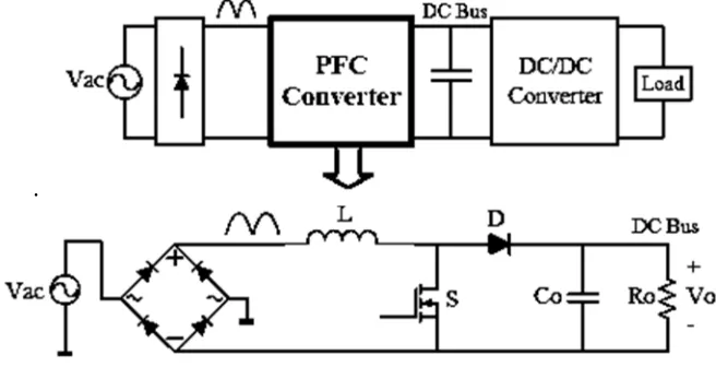
[image:2.612.131.459.466.634.2].
Figure 1: PFC converter
II. PFC MODES OF OPERATION
and also to CCM, without any performance advantage compared to CrCM. For that reason, CrCM is a more common practice design than DCM, therefore, this document will exclude the DCM design. CrCM may be considered a special case of CCM, where the operation is controlled to stay at the boundary between CCM and DCM. CrCM usually uses constant on-time control; the line voltage is changing across the 60 Hz line cycle, the reset time for the boost inductor is varying, and the operating frequency will change as well in order to maintain the boundary mode operation. CrCM dictates the controller to sense the inductor current zero crossing in order to trigger the start of the next switching cycle. The inductor current ripple (or the peak current) in CrCM is twice of the average value, which greatly increases the MOSFET RMS currents and turn-off current.
On the other side, CCM encounters the turn-on losses in the MOSFET, which can be exacerbated by the boost rectifier reverse recovery loss due to reverse recovery charge, Qrr. For this reason, ultra-fast recovery diodes or silicon carbide Schottky diodes with extreme low Qrr are needed for CCM mode. In conclusion, we can say that for low power applications, the CrCM boost has the advantages in power saving and improving power density. This advantage may extend to medium power ranges, however at some medium power level the low filtering ability and the high peak current starts to become severe disadvantages. At this point the CCM boost starts being a better choice for high power applications.
Since this document is intended to support high power PFC applications, therefore a CCM PFC boost converter has been chosen in the application note with detailed design discussions and design examples for demonstration.The current ripple (or the peak current) in CrCM is twice the average value, which greatly increases the RMS currents and turn off current. But since every switching cycle starts at zero current, and usually with ZVS operation, turn on loss is usually eliminated.
III. WORKING OF PFC
Single-phase AC/DC converters are one of the most common power conversion systems and can be found in many industrial as well as residential applications, e.g., variable speed drive, electric vehicle chargers, and power supplies for consumer electronics. In order to meet the ever more stringent grid codes like the IEC61000-3-2 harmonic limits, high-power factor and sinusoidal current regulation are required for basically all such applications as long as their power ratings exceed 75W.
Technology (IJRASET)
Figure.2 Circuit diagram of the proposed three-level PFC converter for single phase PHEV chargers.
However, most of the existing single-phase PFC converters are of boost type and can only provide an output voltage that is higher than the peak voltage of the ac input. Wide range of output voltage is indeed desired in some applications like in Plug-in Hybrid Electric Vehicle (PHEV) charging systems where the terminal voltage of battery packs may vary between 100V and 600V, depending on their configuration and state-of-charge. In this case, a second stage dc/dc buck converter has to be implemented to further step down the PFC output voltage, which undoubtedly decreases the system overall efficiency.
Figure.3 Idealized operating waveforms for the proposed three-level PFC Converter.
Is the root reason that why the dc/dc converter may only process partial input power and higher conversion efficiency can be obtained through the proposed topology. The idealized operating waveforms during these two modes are presented. In order to ensure smooth transition between the low- and high-voltage level commutations, an offset is injected into the carrier of the pulse-width modulation (PWM) for Q2.
Compared with the conventional boost PFC, the proposed converter will have slightly higher conduction losses because of the series connection of Q2 and D1. However, its switching losses can be greatly reduced due to its three-level output that splits the high dc bus voltage into two low voltage portions. Moreover, efficiency gain from the dc/dc converter is also significant because it only converts the input power that flow through D2. To estimate the percentage of input power λ that is converted by this buck stage, it is assumed that the power converter is lossless and harmonic free.
A. Simulation Study
Simulation study was carried out in MATLAB/Simulink environment and the circuit parameters are listed in. The steady-state operation waveforms are presented. It can be seen that Q1 and Q2 operate alternatively and may produce. The desired three-level converter pole voltage VAB. The high level bus voltage is not constant because the dc-link capacitor needs to absorb the system double line frequency harmonic.
Figure.5 Experimental steady-state waveforms under 230-V/2-kW operation,
C1: grid voltage, C2: converter pole voltage, C3: buck converter current, and C4: grid current.
Figure.6 Experimental load step-up waveforms, C1: input voltage, C2: high dc bus voltage, C3: load voltage, and C4: load current.
Mentioned previously, this is because the intermittent operation of the buck converter may impose disturbances to the system and affect the input current regulation under high-line operation. The proposed PFC converter is also compared with a conventional two-stage solution, i.e., a boost PFC cascaded with a dc/dc buck converter, and its circuitry is obtained by removing D1 and Q2. Therefore, the proposed three-level PFC will have higher cost than the conventional one, and it is complicated with one fast recovery diode (D1), one switch (Q2), and one isolated gate driver.
B. Control Technique
Technology (IJRASET)
Fig.4.2 Control technique
Fig.4.3 Input voltage
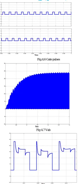
Fig.4.6 Gate pulses
Fig 4.7 Vab
Technology (IJRASET)
Fig.4.9 Output voltage
Fig.4.10 THD for input current
Fig.4.11 Power factor
V. CONCLUSION
[1] Electromagnetic Compatibility (EMC)—Part3: Limits—Section 2: Limits for Harmonic Current Emissions (Equipment Input Current < 16 A PerPhase), IEC Standard 61000-3-2, 1998.
[2] L. Huber, Y. Jang, and M. M. Jovanovic, “Performance evaluation of bridgeless PFC boost rectifiers,” IEEE Trans. Power Electron., vol. 23, no. 3, pp. 1381– 1390, May 2008.
[3] F. Musavi, W. Eberle, and W. G. Dunford, “A high-performance singlephase bridgeless interleaved PFC converter for plug-in hybrid electric vehicle battery chargers,” IEEE Trans. Ind. Appl., vol. 47, no. 4, pp. 1833– 1843, Jul./Aug. 2011.
[4] F. Musavi, M. Edington, W. Eberle, and W. G. Dunford, “Evaluation and efficiency comparison of front end AC–DC plug-in hybrid charger topologies,” IEEE Trans. Smart Grid, vol. 3, no. 1, pp. 413–421, Mar. 2012.
[5] M. Pahlevaninezhad, P. Das, J. Drobnik, P. K. Jain, and A. Bakhshai, “A ZVS interleaved boostAC/DC converter used in plug-in electric vehicles,” IEEE Trans. Power Electron., vol. 27, no. 8, pp. 3513–3529, Aug. 2012.
[6] C. Marxgut, F. Krismer, D. Bortis, and J. W. Kolar, “Ultraflat interleaved triangular current mode (TCM) single-phase PFC rectifier,” IEEE Trans. Power Electron., vol. 29, no. 2, pp. 873–882, Feb. 2014.
[7] D. Aggeler, F. Canales, H. Zelaya, D. L. Parra, A. Coccia, N. Butcher, and O. Apeldoorn, “Ultra-fast dc-charge infrastructures for EV-mobility and future smart grids,” in Proc. IEEE Power Energy Soc. Innovative Smart Grid Technol. Conf. Europe, Oct. 2010, pp. 1–8.
[8] C. S. Moo, K. H. Lee, H. L. Cheng, and W. M. Chen, “A single-stage high-power-factor electronic ballast with ZVS buck–boost conversion,” IEEE Trans. Ind. Electron., vol. 56, no. 4, pp. 1136–1146, Apr. 2009.
[9] R.Watson, G. C. Hua, and F. C. Lee, “Characterization of an active clamp flyback topology for power factor correction applications,” IEEE Trans. Power Electron., vol. 11, no. 1, pp. 191–198, Jan. 1996.
BIOGRAPHY
Mrs. T. Roubavathi, was born on 1990 at Pondicherry. She received her UG in Electrical and Electronics Engineering from Regency Institute of Technology, Yanam, Pondicherry university. She is currently perusing M.Tech Power Systems in PRIST University Pondicherry, Tamil Nadu. Her areas of interests are Power quality issues, and electrical machines.