N A N O E X P R E S S
Open Access
Ab initio
design of nanostructures for solar energy
conversion: a case study on silicon nitride
nanowire
Hui Pan
Abstract
Design of novel materials for efficient solar energy conversion is critical to the development of green energy technology. In this work, we present a first-principles study on the design of nanostructures for solar energy harvesting on the basis of the density functional theory. We show that the indirect band structure of bulk silicon nitride is transferred to direct bandgap in nanowire. We find that intermediate bands can be created by doping, leading to enhancement of sunlight absorption. We further show that codoping not only reduces the bandgap and introduces intermediate bands but also enhances the solubility of dopants in silicon nitride nanowires due to reduced formation energy of substitution. Importantly, the codoped nanowire is ferromagnetic, leading to the improvement of carrier mobility. The silicon nitride nanowires with direct bandgap, intermediate bands, and ferromagnetism may be applicable to solar energy harvesting.
Keywords:Silicon nitride nanowire; Solar energy harvesting; Doping; First-principles calculation
Background
As one of the green energy sources, solar energy has been widely investigated to replace the old forms of depletable energy, such as coal and oil, which are limited on earth and detrimental to global climate. It needs, therefore, to develop reliable technologies to efficiently convert solar energy to other usable energy forms, such as electricity and chemical energy. A few technologies have been devel-oped to harvest solar energy, including photovoltaic cells (PV; converting solar energy to electrical energy), photo-electrochemical cells (PEC; converting solar energy to chemical energy), and solar thermal systems (converting solar energy to thermal energy). In all of these technolo-gies, the fundamental element, materials, plays a dominant role to maximally utilize the sunlight. For photovoltaic cells, the optimum bandgap for the solar cell material is a compromise between a bandgap wide enough so that not too many electrons are wasted and yet narrow enough so that enough photons can be absorbed to cre-ate electron–hole pairs [1]. For photoelectrochemical
cells, the development of an efficient photocatalyst for water splitting requires (a) narrowing its bandgap that satisfies the visible light absorption and the band edge requirement of H2/H2O and O2/H2O levels [2,3] and (b) having high contacting surface area with the electrolyte to enhance the reaction and to increase the light absorption [4]. However, no semiconductor has a bandgap that can utilize the entire spectral distribution of sunlight. To enhance the light absorption efficiency, considerable effort has been conducted for the maximal absorption of sunlight, such as chemical doping [2-8], dye sensitization [9-11], material design [12-14], defect engineering [15-17], and structure engineering [18-20]. However, novel cell concepts are necessary for a huge increase in the effi-ciency. One of the concepts, hot-carrier solar cell, is to use semiconductor nanocrystals or quantum dots to capture all of the energy of hot carriers [21,22], where hot-carrier relaxation is only possible via slower multiphonon emis-sion because of the quantum confinement-induced discre-tized band states in the nanostructures [23]. Another important concept is the intermediate band (IB) solar cell, consisting of an IB material situated between two conven-tional semiconductors, n- and p-types [24-26], where the IB material has a band inside the bandgap. A full electron Correspondence:[email protected]
Institute of Applied Physics and Materials Engineering, Faculty of Science and Technology, University of Macau, Avenida da Universidade, Taipa, Macao SAR, People's Republic of China
transition from the valence band to the conduction band can be completed by means of two photons with energy below the bandgap, resulting in the increase in photocur-rent. The IB can arise from the quantum confinement effects in quantum dots [27-29] or impurity states by dop-ing bulk materials with a transition metal [30-33]. Recently, solar cells based on nanostructures have attracted consid-erable attention because of possible cost reduction and efficiency improvement [34-36]. Therefore, nanostructures possessing an intermediate band and quantum confine-ment effect may be able to enhance the efficiency and reduce the cost at the same time.
Silicon nitride (Si3N4) is a material of great techno-logical interest in a number of applications, such as high-temperature electronics, because of its chemical inertness, high dielectric constant, large electronic gap, high resistance against radiation, and strong resistance against thermal shock [37]. Importantly, Si3N4is a well-known antireflection coating material in the semicon-ductor industry to reduce the light reflection in Si-based solar cells [38]. Also, single-crystal Si3N4nanowires on a Si substrate can be easily synthesized by chemical vapor deposition [39]. It is expected that an energy-harvesting cell based on Si3N4nanowires and the present Si technol-ogy may make the Si3N4-based energy harvesting cell possibly produced on sustainable improved efficiency and cost reduction because of the easy integration of Si3N4 into the Si technology. In this work, we explore the electronic, magnetic, and optical properties of a Si3N4 nanowire for its possible application in solar energy conversion based on first-principles calculation. Our calcu-lations predict that the Si3N4 nanowire is a direct-band semiconductor with reduced bandgap, and IBs can be created by doping with carbon and transition metals. We further show that anion-cation codoping can improve the solubility of a transition metal in Si3N4and its crystallinity and enhance the magnetic moment. We further predict
that the ferromagnetic Si3N4 nanowire with IB is more efficient for solar energy conversion.
Methods
[image:2.595.59.540.547.704.2]To investigate the electronic, optical, and magnetic prop-erties of the Si3N4 nanowire, first-principles calculations are carried out based on the density functional theory (DFT) and the Perdew-Burke-Ernzerhof generalized gradi-ent approximation (PBE-GGA) [40-42]. The Vienna Ab initio Simulation Package (VASP) incorporated with the projector augmented wave (PAW) scheme is used [43,44]. The nanowire is created along theβ-Si3N4[001] direction (Figure 1). An energy cutoff of 450 eV is used for the plane wave expansion of the electronic wave function. The Monkhorst-Pack scheme is used to generate special k
points with a 1 × 1 × 3 grid [45]. Good convergence is obtained with these parameters. The total energy is converged to 2.0 × 10⁻⁵ eV/atom while the Hellmann-Feynman force is smaller than 5.0 × 10⁻² eV/Å in the optimized structure. A large hexagonal supercell with a shortest wall-wall distance of 10 Å in the plane perpen-dicular to the wire axis and four unit cells parallel to the wire axis is used to avoid interactions between the wire and its images in neighboring cells and between dopants. The nanowire has 96 nitrogen and 72 silicon atoms.
To study the optical property of the nanowire, we calculate the loss function, which is a direct probe of the collective excitation of the system under consider-ation. The imaginary part of the dielectric constant is calculated from:
ε2ðq→O⌢u;ℏωÞ ¼
2e2π Ωε0
X
k;v;c <Ψc
k
⌢
u⋅rjΨvk
>j2δ
Eck−Evk−E
ð1Þ
where⌢u is the vector defining the polarization of the in-cident electric field. This expression is similar to Fermi's
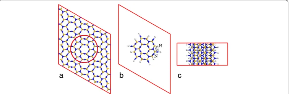
Figure 1Schematic drawings of the atomic structures ofβ-Si3N4bulk (a) and nanowire: (b) top and (c) side views.The red circle in
golden rule for time-dependent perturbations, and ε2(ω) can be thought of as detailing the real transitions between occupied and unoccupied electronic states. The real part,
ε1(ω), is obtained by the Kramers-Kronig relation. The loss function is calculated using Im(−1/ε(ω)) at zero momen-tum transfer from the macroscopic dielectric functionε(ω) (ε(ω) =ε1(ω) +iε2(ω)) for a periodic system.
Results and discussion
β-Si3N4bulk
The periodic unit cell ofβ-Si3N4is optimized first to obtain the lattice parameters. The lattice constants of the opti-mized structure (a =7.613 Å, c= 2.910 Å) within PBE-GGA are in good agreement with the experimental values (a =7.608 Å, c= 2.909 Å) [37]. β-Si3N4 is an indirect-bandgap semiconductor with the valence band top (VBT) at one third along the Γ-A axis and the conduction band bottom (CBB) at the Γpoint (Figure 2a). The calculated bandgap is 4.25 eV within PBE-GGA (Figure 2), which is consistent with the reported data (4.2 eV) [46], but less than the experimental value (5.3 eV) due to the underesti-mation of the bandgap by density functional theory. The analysis on the partial density of states (PDOS) reveals that the VBT states are mainly dominated by N_p electrons, while Si_p electrons mainly contribute to the CBB states (Figure 2b).
β-Si3N4nanowire
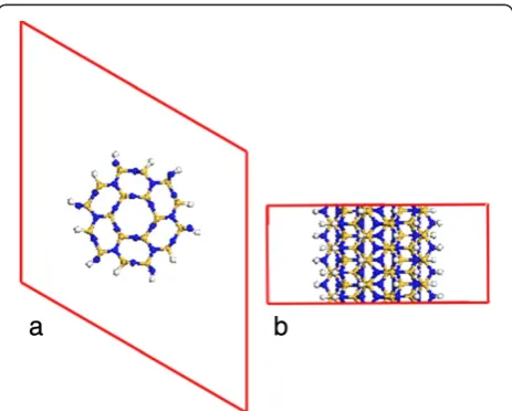
The β-Si3N4 nanowire is modeled by cutting the bulk supercell along the [001] direction (Figure 1a). The surface atoms are passivated by hydrogen atoms (totally 48 H atoms in the supercell) (Figure 1b,c). The structure of the optimized Si3N4 nanowire almost keeps unchanged, except the hydrogen atoms at the surface (Figure 3). The Si-N bond length is expanded by less than 1%. The Si-H and N-H bond lengths are 1.489 and 1.019 Å, respectively. The calculated electronic property of the nanowire shows a notable feature in its band structure (Figure 4).
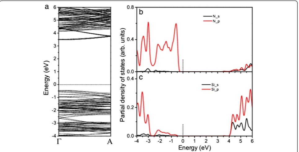
The nanowire is a direct-bandgap semiconductor with both the VBT and CBB at the Γ point. Compared with those in the band structure ofβ-Si3N4bulk along theΓ-A axis, the valence band top states in that of the nanowire are pushed up, especially the states at theΓpoint, leading to almost flat bands from theΓpoint to one third of the
Γ-A axis (VBT in the band structure of β-Si3N4 bulk) (Figures 2a and 4a) and the occurrence of VBT at the Γ point. The change of the VBT states is attributed to the confinement of charge carriers which results in the quasi-continuous energy bands of the bulk semiconductors becoming discretized. The VBT states are still dominated by N_pelectrons (Figure 4b). The CBB remains at theΓ point with the parts of the CBB states in the nanowire pulled down. In contrast to the β-Si3N4 bulk, the p
[image:3.595.59.541.89.254.2]electrons from both N and Si contribute to the CBB states in the nanowire (Figure 4b,c). The up-shift of VBT and down-shift of CBB lead to the reduction of bandgap Figure 2Calculated band structure (a) and partial density of states (b) ofβ-Si3N4bulk.
Figure 3The optimized atomic structures ofβ-Si3N4nanowire
[image:3.595.306.538.516.702.2](3.92 eV). The direct band structure in the nanowire may enhance the conversion efficiency due to the improvement of carrier transportation. However, the bandgap of the nanowire is still too larger to be efficient of the sunlight absorption. It is necessary to engineer the bandgap to im-prove the absorption.
Single-element-dopedβ-Si3N4nanowire
One of the important ways to engineer the bandgap of semiconductors is to create intermediate bands within the gap by doping. Three elements, oxygen, carbon, and chro-mium, are studied because the contamination of oxygen and carbon easily occurs in the growth of Si3N4and chro-mium is the most possible element for the creation of IB in the bandgap [31,32]. The doping is modeled by substitut-ing a cation atom with a chromium atom or an anion atom with an oxygen or carbon atom inside the nanowire. As an indication of the doping possibility and stability, the doping formation energy is estimated from [47]:
Ef ¼EtotðNWþdopingÞ−EtotðNWÞ−μdopantþμhost
ð2Þ
whereEtot(NW+doping) andEtot(NW) are the total en-ergies of the β-Si3N4nanowire (NW) with and without doping, respectively. μdopant and μhost are the energies of dopants (O, C, Cr, CrO, or CrC) and host atoms (Si, N, or SiN), respectively. μO¼1
2μð ÞO2 , μN¼12μð ÞN2 ,
μCr=μ(CrBulk), μSi=μ(SiBulk) and μC=μ(graphite). The
formation energies of single-element doping (Table 1) indicate that the Cr atoms prefer to take the cation po-sitions (Si sites), while the O and C atoms substitute the anion positions (N sites) more easily, because of the rela-tively lower formation energies. The formation energy for oxygen substituting nitrogen is only 0.75 eV, indicating that the doping of oxygen is much easier than that of other elements. The calculated bond lengths for the stable doping states are 1.799 Å for the O-Si bond, 1.826 Å for the C-Si bond, and 1.845 Å for the Cr-N bond in O-, C-, and Cr-doped nanowires, respectively, which are larger than the Si-N bond length (1.741 Å). The least change in the structure of the O-doped nanowire is consistent with lower doping energy.
The calculated band structure shows that the O-doped
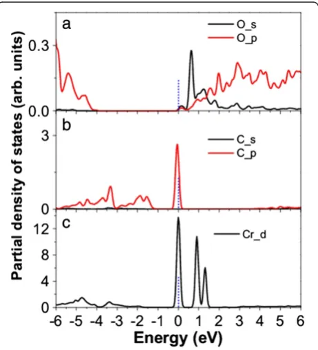
[image:4.595.58.541.89.335.2]β-Si3N4nanowire is an n-type semiconductor with a direct bandgap of 3.89 eV at theΓpoint (Figure 5a). The PDOS analysis shows that thesandpelectrons are also involved in the CBB states (Figure 6a). The band structure of the O-doped nanowire is similar to that of the undoped nano-wire, except that the Fermi level is within the conduction band because of the contributed electrons from oxygen, indicating that O doping cannot efficiently narrow the Figure 4Calculated band structure (a) and PDOS for N (b) and Si (c) ofβ-Si3N4nanowire.
Table 1 Formation energy for the various doping configurations in theβ-Si3N4nanowire
O-s-Si O-s-N C-s-Si C-s-N Cr-s-Si Cr-s-N
Ef(eV) 10.25 0.75 5.11 3.62 3.81 8.50
For example, O-s-Si means that O substitutes Si.
[image:4.595.303.542.699.724.2]bandgap of the nanowire. An intermediate level with less dispersion is formed by C doping, crossing the Fermi level (Figure 5b), which is dominated by the C_p electrons (Figure 6b). The gaps between the IB and VBT or CBB are 0.96 and 2.96 eV, respectively. Three IBs are formed by Cr doping, which separate the bandgap into four regions with the gaps of 1.68, 0.92, 0.42, and 0.88 eV from the VBT to CBB, respectively (Figure 5c). The impurity states are
mainly attributed to the Cr_d electrons (Figure 6c). The Cr_d electrons should form a quasi-continuous impurity band inβ-Si3N4bulk, which are discretized in the nanowire due to the quantum confinement effect. The creation of IB by doping, especially Cr doping, should improve the sunlight absorption of the nanowire.
The calculated loss functions of the β-Si3N4nanowires clearly demonstrate the improvement of the light absorp-tion, especially the C- and Cr-doped nanowires (Figure 7). The intercept in the loss function is the optical gap and related to the inter-band excitation. Comparing the loss functions ofβ-Si3N4bulk and nanowire (Figure 7a,b), we see that the light absorption in the nanowire is redshifted because of the reduced bandgap. For the O-doped nano-wire, an absorption peak starting from 0 eV is attributed to the electron excitation near the Fermi level because the O-doped nanowire is an n-type semiconductor (Figure 5a). The loss function of the C-doped β-Si3N4 nanowire is similar to that of the undoped one, except for a weak peak at 2.1 eV (Figure 7c), which is related to the inter-band excitation from VBT to IB or from IB to CBB (Figure 5b). For the Cr-doped nanowire, the loss function clearly shows that the excitation starts at 2.3 eV. From the loss functions of the doped nanowires, we can see that the IBs within the gap improve the absorption of the sunlight because of the reduced inter-bandgap (Figure 5c).
Anion-cation-codopedβ-Si3N4nanowire
[image:5.595.59.540.89.295.2]The codoping is realized by simultaneously substituting a cation atom with a chromium atom and an anion atom with an oxygen or carbon atom as a pair inside the nanowire. The calculated formation energies are 1.51 and 6.06 eV for CrO and CrC codoping, respectively. The formation energy of CrO codoping is much lower than Figure 5Calculated spin-unpolarized band structures ofβ-Si3N4nanowires doped with (a) O, (b) C, and (c) Cr.
Figure 6Calculated spin-unpolarized PDOS ofβ-Si3N4nanowires
[image:5.595.59.290.452.706.2]that of Cr doping because of the electrostatic attraction of the two dopants with opposite charge states [31,32], which indicates that the Cr substitution can be greatly enhanced in the presence of O doping and results in the enhance-ment of solubility of Cr in the nanowire and improveenhance-ment of crystallinity. However, the CrC codoping is unstable be-cause of electrostatic repulsion between the two dopants, as indicated by the high formation energy, and will not be discussed. The Cr-N, Si-O, and Cr-O bond lengths in the CrO-codoped nanowire are 1.889, 1.703, and 1.996 Å, respectively.
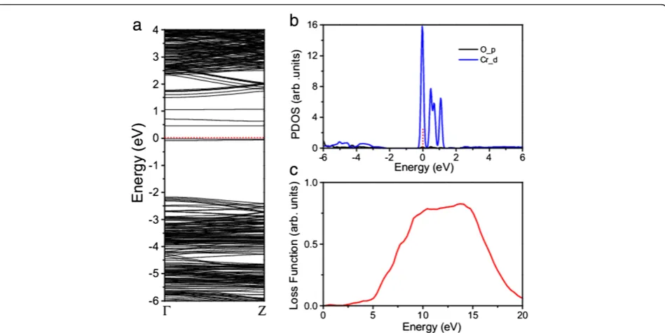
The calculated electronic and optical properties of the CrO-codoped β-Si3N4 nanowire show that four IBs are observable in the bandgap (Figure 8a), which are domi-nated by the Cr_d electrons (Figure 8b). The space between the VBT and the first IB is about 2.1 eV. Com-pared with those in the Cr-doped nanowire, the Cr_d
electrons in the CrO-codoped nanowire are more discretized due to the quantum confinement effect and the strong coupling between the Cr_d and O_p elec-trons (Figure 8b). A similar situation occurs at the conduction band bottom, where more states become degen-erate. Similar to Cr-doped nanowire, CrO-codoped nano-wire also shows a excitation about at 2.3 eV (Figure 8c).
Magnetic properties of Cr-doped and CrO-codoped
β-Si3N4nanowires
[image:6.595.58.292.89.410.2]To investigate the magnetic properties of the doped nanowires, spin-polarized calculations are performed. To study the magnetic coupling between metal dopants, two neighboring Si atoms in the nanowire are substituted by
[image:6.595.62.537.476.714.2]Figure 8Calculated spin-unpolarized band structure (a), PDOS (b), and loss function (c) ofβ-Si3N4nanowire codoped with CrO.
Figure 7Calculated loss functions ofβ-Si3N4bulk (a), nanowire
(b), and nanowires doped with (c) O, (d) C, and (e) Cr.
two Cr atoms (Cr2) for the Cr-doped nanowire, and two neighboring Si atoms and one N atom bonded with them are replaced by two Cr atoms and one O atom (Cr2O) for the codoped nanowire. The calculated exchange energies, defined by the energy difference between the antiferromag-netic and ferromagantiferromag-netic states (Eexch=EAFM−EFM), are 135 and 293 meV for the Cr2-doped and Cr2O-codoped nanowires, respectively, indicating that the nanowires with doping are ferromagnetic. Importantly, the exchange en-ergy of the codoped nanowire is much larger than that of the Cr-doped nanowire, leading to a much stable ferro-magnetic state and higher transition Curie temperature of the codoped nanowire. The calculated magnetic moments per Cr atom are 1.85 and 2.29 μBfor the Cr-doped and CrO-codoped nanowires, respectively. Clearly, the codop-ing enhances not only the exchange energy but also the magnetic moment.
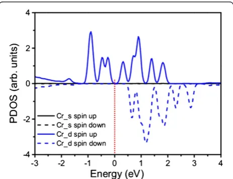
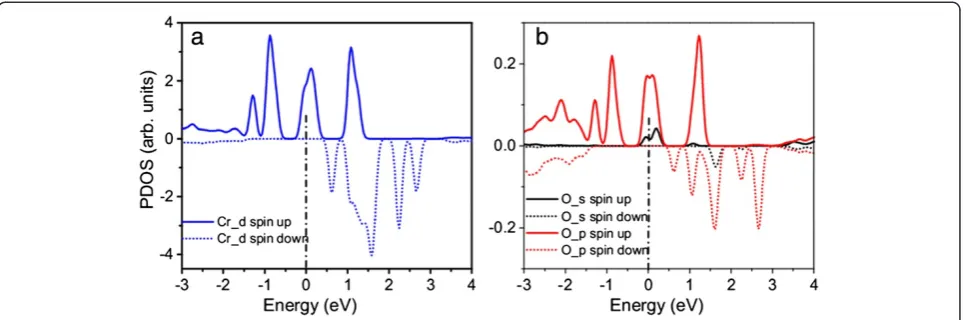
The calculated unsymmetrical spin-up and spin-down total density of states (DOS) confirm the ferromagnet-ism of the Cr-doped (Figure 9a) and CrO-codoped (Figure 9b) β-Si3N4 nanowires. All of these spin-polarized electrons are within the spin-up bands. For the Cr-doped nanowire, several impurity bands are observable and the Fermi level is in the gap between two impurity bands in the spin-up band (Figure 9a). The impurity states form three bands in the spin-up band, and the Fermi level is within the second impurity band when Cr codoped with oxygen (Figure 9b), indi-cating stronger polarization and enhancement of the magnetic moment. The PDOS analysis shows that the impurity states are mainly attributed to the spin-polarized Cr_d electrons for the Cr-doped nanowire (Figure 10), and for the CrO-codoped nanowire, the spin-polarized Cr_d and O_p electrons dominate the impurity bands (Figure 11). The Cr_d electrons strongly hybridized with the O_p electrons in the codoped nano-wire, resulting in the stabilization of parallel spin align-ment. The spin-polarized states within the bandgap
(Figure 9) reveal that double exchange, which is stabi-lized by carrier (electrons) mediation, is the dominant coupling mechanism for the ferromagnetism in the Cr-doped and CrO-coCr-doped nanowires [48-52]. That is, given the incomplete filling of bands, when the ex-change splitting is bigger than the bandwidth, the band energy of the ferromagnetic state is lower than that of the antiferromagnetic state if a sufficient (usually rather small) number of holes (or electrons) exists [49]. The exchange splitting is bigger than the valence band (Figure 9), and there are a considerable number of car-riers. We can therefore conclude that carrier-mediated double exchange is responsible for the observed ferro-magnetism in the Cr-doped and CrO-codoped β-Si3N4 nanowires.
[image:7.595.59.541.89.247.2]The calculated electronic structures (Figure 9) further reveal the enhancement of the sunlight absorption in the doped nanowires because of the formation of IBs within the bandgap. Importantly, the diluted magnetic
Figure 10Calculated spin-polarized PDOS ofβ-Si3N4nanowire
[image:7.595.306.538.525.703.2]with Cr doping.
semiconductors (DMSs) with IBs can have the desired optical properties and prevent radiative transition by taking the advantage of spin selection rules on IB transition [33]. The carrier mobility/lifetime is greatly enhanced because the spin degeneracy of the bands is lifted in DMSs and the unwanted recombinations are impeded by spin selection rules or by low occupancy of states involved in the allowed recombinations [53,54]. All of these advantages lead to the enhancement of the conversion efficiency of magneticβ-Si3N4nanowires.
Conclusions
In summary, a first-principles design of nanostructures is carried out to investigate their applications in solar energy harvesting. The calculated results show that the band structures of bulk materials can be engineered by reducing their size. Bulk Si3N4 is an indirect-bandgap semicon-ductor, while Si3N4nanowire is a direct one. We show that the band structure of the nanowire can be further controlled by doping. Intermediate bands within its bandgap can be created by doping. The calculated op-tical property shows that the intermediate bands play an important role in the enhancement of visible light absorption. We also show that anion-cation codoping is easier than single-element doping because of the elec-trostatic attraction of the anion and cation. We further demonstrate that the ferromagnetic nanowire can be real-ized by codoping, where spin polarization can efficiently improve carrier mobility due to spin selection rules. The designed nanowire with a controllable band structure engineered by doping and size reduction shows efficient sunlight absorption and improved mobility and may find applications in solar energy harvesting.
Competing interests
The author declares that he has no competing interests.
Acknowledgements
Hui Pan thanks the supports of the Science and Technology Development Fund from Macao SAR (FDCT-076/2013/A) and Multi-Year Research Grant (MYRG2014-00159-FST) and Start-up Research Grant (SRG-2013-00033-FST) from the Research & Development Office at the University of Macau. The DFT calculations were performed at the High-Performance Computing Cluster (HPCC) of the Information and Communication Technology Office (ICTO) at the University of Macau.
Received: 25 August 2014 Accepted: 20 September 2014 Published: 26 September 2014
References
1. Moller HJ:Semiconductors for Solar Cells.Boston: Artech House; 1993. 2. Chen X, Mao SS:Titanium dioxide nanomaterials: synthesis, properties,
modifications, and applications.Chem Rev2007,107:2891–2959. 3. Lee ASH, Li K, Zhang YW, Pan H:Ab initio study on the effects of
dopant-defect cluster on the electronic properties of TiO2-based photocatalysts.Int J Hydro Energy2014,39:2049–2055.
4. Dou MF, Baldissera G, Persson C:ZnO–InN nanostructures with tailored photocatalytic properties for overall water-splitting.Int J Hydro Energy 2013,38:16727–16732.
5. Asahi A, Morikawa T, Ohwaki T, Aoki K, Taga Y:Visible-light photocatalyst in nitrogen-doped titanium oxides.Science2001,293:269–271. 6. Borgarello E, Kiwi J, Gratzel M, Pelizzetti E, Visca M:Visible light induced
water cleavage in colloidal solutions of chromium-doped titanium dioxide particles.J Am Chem Soc1982,104:2996–3002.
7. Gao MQ, Xu YL, Bai Y, Xiao F:Nb, F-codoped TiO2hollow spheres with high visible light photocatalytic activity.Nanoscale Res Lett2013,8:508. 8. Tan LL, Ong WJ, Chai SP, Mohamed AR:Reduced graphene oxide-TiO2
nanocomposite as a promising visible-light-active photocatalyst for the conversion of carbon dioxide.Nanoscale Res Lett2013,8:465.
9. Wang XL, Wu M, Ding J, Li ZS, Sun KN:Periodic density functional theory study on the interaction mode and mechanism of typical additives with TiO2substrates for dye-sensitized solar cell applications.J Power Sources 2014,246:10–18.
10. Lim J, Ryu SY, Kim J, Jun Y:A study of TiO2/carbon black composition as counter electrode materials for dye-sensitized solar cells.Nanoscale Res Lett2013,8:227.
11. Luo Y, Li D, Meng Q:Towards optimization of materials for dye-sensitized solar cells.Adv Mater2009,21:1–5.
12. Lim YK, Koh EWK, Zhang YW, Pan H:Ab initio design of GaN-based photocatalyst: ZnO-codoped GaN nanotubes.J Power Sources2013, 232:323–331.
13. Punya A, Lambrecht WRL:Band offsets between ZnGeN2, GaN, ZnO, and ZnSnN2and their potential impact for solar cells.Phys Rev B2013,88:075302. 14. Yang SY, Seidel J, Byrnes SJ, Shafer P, Yang CH, Rossell MD, Yu P, Chu YH,
[image:8.595.58.541.89.249.2]Scott JF, Ager JW, Martin LW, Ramesh R:Above-bandgap voltages from ferroelectric photovoltaic devices.Nat Nanotech2010,5:143–147.
Figure 11Calculated spin-polarized PDOS ofβ-Si3N4nanowire with CrO codoping for (a) Cr and (b) O.
15. Pan H, Guo B, Zhang ZY:Phase-dependent photocatalytic activity of TiO2: a first-principles study.J Chem Theory Comput2009,5:3074–3078. 16. Nowotny MK, Sheppard LR, Bak T, Nowotny J:Defect chemistry of titanium
dioxide. Application of defect engineering in processing of TiO2-based photocatalyst.J Phys Chem C2008,112:5275–5300.
17. Pan H, Qiu X, Ivanov IN, Meyer HM, Wang W, Zhu WG, Paranthaman MP, Zhang ZY, Eres G, Gu B:Fabrication and characterization of brookite-rich, visible light-active TiO2 films for water splitting.Appl Catal B Environ 2009,93:90–95.
18. Sun B, Shi TL, Peng ZC, Sheng WJ, Jiang T, Liao GL:Controlled fabrication of Sn/TiO2nanorods for photoelectrochemical water splitting. Nanoscale Res Lett2013,8:462.
19. Pala RA, White J, Barnard E, Liu J:Design of plasmonic thin-film solar cells with broadband absorption enhancements.Adv Mater2009,21:1–6. 20. Sato H, Matsuda R, Sugimoto K, Takata MS:Photoactivation of a
nanoporous crystal for on-demand guest trapping and conversion.Nat Mater2010,9:661–666.
21. Tisdale WA, Williams KJ, Timp BA, Norris DJ, Aydil ES, Zhu ZY:Hot-electron transfer from semiconductor nanocrystals.Science2010,328:1543–1547. 22. Alivisatos AP:Semiconductor clusters, nanocrystals, and quantum dots.
Science1996,271:933–937.
23. Nozik AJ:Spectroscopy and hot electron relaxation dynamics in semiconductor quantum wells and quantum dots.Annu Rev Phys Chem 2001,52:193–231.
24. Luque A, Marti A:Increasing the efficiency of ideal solar cells by photon induced transitions at intermediate levels.Phys Rev Lett1997, 78:5014–5017.
25. Luque A, Marti A:The intermediate band solar cell: progress toward the realization of an attractive concept.Adv Mater2010,22:160–174. 26. Wang WM, Lin AS, Phillips JD:Intermediate-band photovoltaic solar cell
based on ZnTe:O.Appl Phys Lett2009,95:011103.
27. Marti A, Lopez N, Antolin E, Canovas E, Luque A, Stanley CR, Farmer CD, Diaz P:Emitter degradation in quantum dot intermediate band solar cells.Appl Phys Lett2007,90:233510.
28. Hubbard SM, Cress CD, Bailey CG, Raffaelle RP, Bailey SG, Wilt DM:Effect of strain compensation on quantum dot enhanced GaAs solar cells.
Appl Phys Lett2008,92:123512.
29. Oshima R, Takata A, Okada Y:Strain-compensated InAs/GaNAs quantum dots for use in high-efficiency solar cells.Appl Phys Lett2008,93:083111. 30. Palacios P, Aguilera I, Sanchez K, Conesa JC, Wahnon P:
Transition-metal-substituted indium thiospinels as novel intermediate-band materials: prediction and understanding of their electronic
properties.Phys Rev Lett2008,101:04640.3.
31. Pan H, Gu B, Eres G, Zhang ZY:Ab initiostudy on non-compensated CrO codoping of GaN for enhanced solar energy conversion.J Chem Phys 2010,132:104501.
32. Zhu WG, Qiu X, Iancu V, Chen XQ, Pan H, Wang W, Dimitrijevic NM, Rajh T, III HM, Paranthaman MP, Stocks GM, Weitering H, Gu B, Eres G, Zhang ZY: Band gap narrowing of titanium oxide semiconductors by
noncompensated anion-cation codoping for enhanced visible-light photoactivity.Phys Rev Lett2009,103:226401.
33. Olea J, Toledano-Luque M, Pastor D, Gonzalez-Diaz G, Martil I:Titanium doped silicon layers with very high concentration.J Appl Phys2008, 104:016105.
34. Tsakalakos L:Nanostructures for photovoltaics.Mater Sci Eng R2008, 62:75–189.
35. Kelzenberg MD, Boettcher SW, Petykiewicz JA, Turner-Evans DB, Putnam MC, Warren EL, Spurgeon JM, Briggs RM, Lewis NS, Atwater HA:Enhanced absorption and carrier collection in Si wire arrays for photovoltaic applications.Nat Mater2010,9:239–244.
36. Chakrapani V, Thangala J, Sunkara MK:WO3and W2N nanowire arrays for photoelectrochemical hydrogen production.Int J Hydro Energy2009, 34:9050–9059.
37. Habraken FHPM, Kuiper AET:Silicon nitride and oxynitride films.
Mat Sci Eng R1994,12:123–175.
38. El Amrani A, Menous I, Mahiou L, Tadjine R, Touati A, Lefgoum A:Silicon nitride film for solar cells.Renew Energy2008,33:2289–2293.
39. Farjas J, Rath C, Pinyol A, Roura P, Bertran E:Si3N4single-crystal nanowires grown from silicon micro- and nanoparticles near the threshold of passive oxidation.Appl Phys Lett2005,87:192114.
40. Hohenberg P, Kohn W:Inhomogeneous electron gas.Phys Rev1964, 136:B864–B871.
41. Perdew JP, Burke K, Ernzerhof M:Generalized gradient approximation made simple.Phys Rev Lett1996,77:3865–3868.
42. Blöchl PE:Projector augmented-wave method.Phys Rev B1994, 50:17953–17979.
43. Kresse G, Furthmüller J:Efficient iterative schemes for ab initio total-energy calculations using a plane-wave basis set.Phys Rev B1996, 54:11169–11186.
44. Kresse G, Joubert D:From ultrasoft pseudopotentials to the projector augmented-wave method.Phys Rev B1999,59:1758–1775.
45. Monkhorst HJ, Pack J:Special points for Brillouin-zone integrations.
Phys Rev B1976,23:5188–5192.
46. Liu AY, Cohen ML:Structural properties and electronic structure of low-compressibility materials:β-Si3N4and hypotheticalβ-C3N4. Phys Rev B1990,41:10727–10734.
47. Zhang SB:The microscopic origin of the doping limits in semiconductors and wide-gap materials and recent developments in overcoming these limits: a review.J Phys Condens Matter2002,14:R881–R903.
48. Pan H, Yi J, Shen L, Wu R, Yang J, Lin J, Feng YP, Ding J, Van LH, Yin JH: Room temperature dilute magnetic semiconductor in carbon-doped ZnO.Phys Rev Lett2007,99:127201.
49. Akai A:Ferromagnetism and its stability in the diluted magnetic semiconductor (In, Mn)As.Phys Rev Lett1998,81:3002–3005. 50. Pan H, Feng YP, Wu Q, Huang Z, Lin J:Magnetic property of carbon
doped CdS: a first-principles and Monte Carlo study.Phys Rev B2008, 77:125211.
51. Dalpian GM, Wei SH:Carrier-mediated stabilization of ferromagnetism in semiconductors: holes and electrons.Phys Stat Sol B2006,243:2170–2187. 52. Pan H, Zhang YW, Shenoy V, Gao HJ:Controllable magnetic property of
SiC by anion-cation codoping.Appl Phys Lett2010,96:192510. 53. Olsson P, Domain C, Guillemoles JF:Ferromagnetic compounds for high
efficiency photovoltaic conversion: the case of AlP:Cr.Phys Rev Lett2009, 102:227204.
54. Pan H, Zhang YW:GaN-ZnO superlattice nanowires as photocatalyst for hydrogen generation: a first-principles study on electronic and magnetic properties.Nano Energ2012,1:488–493.
doi:10.1186/1556-276X-9-531
Cite this article as:Pan:Ab initiodesign of nanostructures for solar energy conversion: a case study on silicon nitride nanowire.Nanoscale
Research Letters20149:531.
Submit your manuscript to a
journal and benefi t from:
7Convenient online submission 7Rigorous peer review
7Immediate publication on acceptance 7Open access: articles freely available online 7High visibility within the fi eld
7Retaining the copyright to your article