N A N O E X P R E S S
Open Access
Ultra-Low Specific On-resistance Lateral
Double-Diffused
Metal-Oxide-Semiconductor Transistor with Enhanced
Dual-Gate and Partial P-buried Layer
Zhuo Wang, Zhangyi
’
an Yuan, Xin Zhou
*, Ming Qiao, Zhaoji Li and Bo Zhang
Abstract
An ultra-low specific on-resistance (Ron,sp) lateral double-diffused metal-oxide-semiconductor transistor (LDMOS) with enhanced dual-gate and partial P-buried layer is proposed and investigated in this paper. On-resistance analytical model for the proposed LDMOS is built to provide an in-depth insight into the relationship between the drift region resistance and the channel region resistance. N-buried layer is introduced under P-well to provide a low-resistance conduction path and reduce the resistance of the channel region significantly. Enhanced dual-gate structure is formed by N-buried layer while avoiding the vertical punch-through breakdown in off-state. Partial P-buried layer with optimized length is adopted under the N-drift region to extend vertical depletion region and relax the electric field peak in off-state, which enhances breakdown voltage (BV) with low drift region resistance. For the LDMOS with enhanced dual-gate and partial P-buried layer, the result shows thatRon,spis 8.5 mΩ·mm2while BV is 43 V.
Keywords:Enhanced dual-gate, Lateral double-diffused metal-oxide-semiconductor transistor (LDMOS), Partial buried layer, Specific on-resistance
Background
With the increase of demand for more complex and faster logic function in analog power IC, it is significant to im-prove the performance of the lateral double-diffused metal-oxide-semiconductor transistor (LDMOS), specially minimizing specific on-resistance (Ron,sp) and maximizing
off-state breakdown voltage (BV) [1–9]. Most developed technologies focus on the drift region optimizing to im-prove the trade-off of Ron,sp vs. BV for LDMOS devices
[10–20]. In our previous work, the LDMOS with ultra-shallow trench isolation (USTI) was proposed [21]. The depth and corner angel of USTI were optimized to achieve best-in-class performance. However, for the low voltage LDMOS, the drift region is losing domination in Ron,sp
and the contribution of the channel region cannot be ignored.
Method
In this work, a novel ultra-low specific on-resistance LDMOS with enhanced dual-gate and partial P-buried layer is investigated. The physical models IMPACT.I, BGN, CONMOB, FLDMOB, SRH, and SRFMOB are used in numerical simulation. On-resistance analytical model is proposed to provide an in-depth insight into the relationship between the drift region resistance and the channel region resistance. Based on the model, N-buried layer and partial P-buried layer are optimized to achieve lowRon,spand high BV.
Results and Discussion
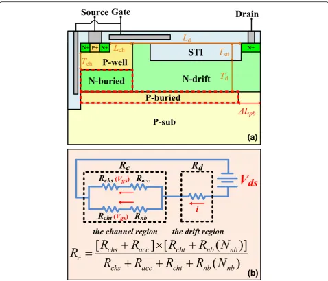
Figure1a shows the schematic cross-section of ultra-low specific on-resistance LDMOS with enhanced dual-gate and partial P-buried layer. The LDMOS features the dual-gate with N-buried layer and the partial P-buried layer which contributes to reduce Ron,sp and enhance
BV, respectively. In the channel region, the enhanced dual-gate is formed by trench gate and highly doped * Correspondence:[email protected]
State Key Laboratory of Electronic Thin Films and Integrated Devices, University of Electronic Science and Technology of China, Chengdu 610054, Sichuan, China
© The Author(s). 2019Open AccessThis article is distributed under the terms of the Creative Commons Attribution 4.0 International License (http://creativecommons.org/licenses/by/4.0/), which permits unrestricted use, distribution, and reproduction in any medium, provided you give appropriate credit to the original author(s) and the source, provide a link to the Creative Commons license, and indicate if changes were made.
Wanget al. Nanoscale Research Letters (2019) 14:38
N-buried layer. Compare to conventional dual-gate structure, N-buried layer significantly reduce the resist-ance of the channel region by provide a low on-resis-tance conduction path under P-well in the on-state. In the drift region, the partial P-buried layer with high dop-ing concentration is introduced under the N-drift region to enhance BV while maintaining low Ron,sp. The partial
P-buried layer helps to reduce the vertical electric field in the off-state without breaking charge balance in the drift region. The key size of the novel device is listed in Table1.
Figure1b shows the schematic equivalent on-resistance model for the proposed LDMOS. The total on-resistance is considered as the resistance of the drift region (Rd) and
the resistance of the channel region (Rc) in series. In the
channel region, surface channel conduction path parallels
the trench channel conduction path. Thus,Rcis equal to
(Rchs+Racc)//(Rcht+Rnb), where Rchs, Racc, Rcht, and Rnb
are the resistances of the surface-gate channel, the accu-mulation region, the trench gate channel, and the N-buried layer, respectively. Based on the proposed on-resistance model, the reduction ofRcwould achieve by
decreasingRnbwithout affecting the other performances,
[image:2.595.58.537.86.496.2]because the other resistances are mainly determinate by
Table 1The key size of the novel device
Ld 1.6μm
Lch 0.3μm
Tch 0.2μm
Tsti 0.3μm
Td 0.7μm
(a)
(b)
[image:2.595.305.538.663.732.2]the process technology, operation voltage, and threshold voltage. TheRdhas been reduced by introducing P-buried
layer under N-drift region to enhance the Reduce Surface-field (RESURF) effect in our previous work. In this work, the partial P-buried layer is adopted to improve the BV while maintaining the lowRd.
Aiming at the reduction ofRc, the N-buried layer with
high doping concentration is introduced under P-well. Figure2 shows numerical and analyticalRcas functions
of the doping concentration of the N-buried layer (Nnb)
with single-gate and dual-gate. It is indicated that the
dual-gate structure helps to reduce Rc compared with
the single-gate. When Nnb=Nd= 5.5 × 1016cm−3, Rc is
110 mΩ. According to the on-resistance model, Rnb is
the main contributor toRc. And then, theRnbis desired
to decrease with the aim of smaller Rc. As shown in
Fig.2a,Rc is reduced with Nnb increasing. When Nnb=
1.35 × 1017cm−3,Rcis reduced to 85 mΩ. However, Fig.2
also shows that Nnbwould be limited by punch-through
breakdown. Because of adding trench gate, Rc is
de-creased firstly by 34% with Nnb=Nd= 5.5 × 1016cm−3.
As Nnbincreases,Rccontinuously decreases. With
opti-mized Nnb= 1.05 × 1017cm−3, Rc is decreased by 45% at
last. WhenNnb> 1.05 × 1017cm−3, punch-through
break-down will happen in P-well. The analytical result of
Ron,spshown in Fig. 2indicates that the proposed model
provides a good fitting with numerical simulation re-sults. Therefore, the model is believable to guide the optimization design.
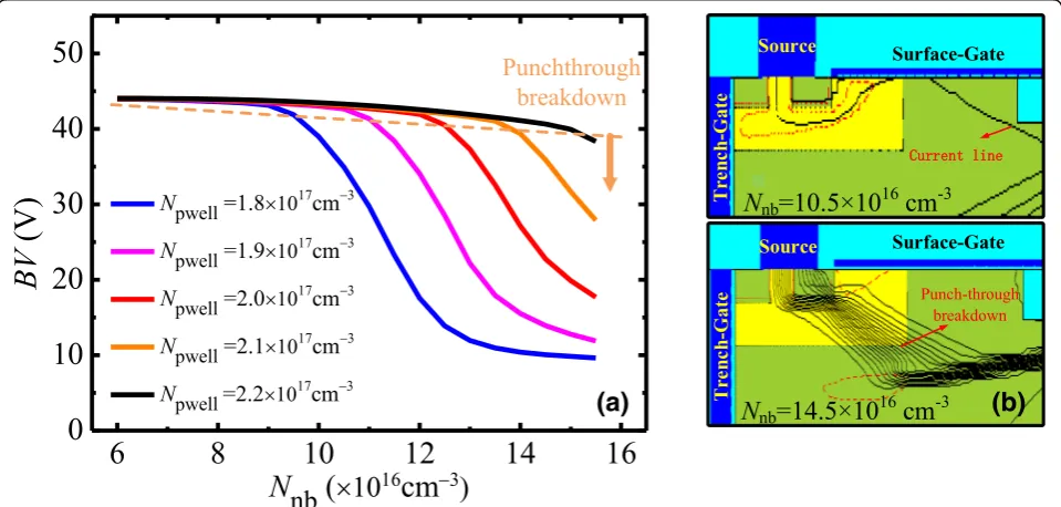
Figure 3a shows numerical BV as a function of Nnb
with different doping concentration of P-well (Npwell). Nnb has an effect on not only the Rc, but also the BV.
For a given Npwell, BV keeps unchanged at small Nnb,
and then decreases with Nnb increasing. When Nnb
in-creases to 1.2 × 1017cm−3, BV starts to drop withNpwell
= 2 × 1017cm−3. The drop of BV is ascribed to punch -through breakdown in the P-well region as shown in Fig. 3b. As drain voltage increases, the depletion region in P-well extends to the source. When the depletion re-gion attacks the N+/P-well junction, the punch-through breakdown occurs. For a largeNpwell, the depletion mainly
extends to the drift region, and the punch-through
Fig. 2Numerical and analyticalRcas a function ofNnbwith
single-gate and dual-single-gate (Z= 1 cm).Ndis the doping concentration of the
N-drift region
(b)
(a)
Fig. 3aNumerical BV as a function ofNnbwith differentNpwell.bCurrent density profile forNnb= 10.5 × 1016cm−3and 14.5 × 1016cm−3while
Npwell= 2 × 1017cm−3at breakdown
[image:3.595.57.290.87.267.2] [image:3.595.58.538.473.702.2]breakdown is avoided without degrading the BV. Al-though P-well with high doping concentration benefits to avoid the punch-through breakdown, it would enhance the threshold voltage. Thus, Npwell of 2 × 1017cm−3 is
chosen with consideration to threshold voltage and the trade-off between the BV andRon,sp.
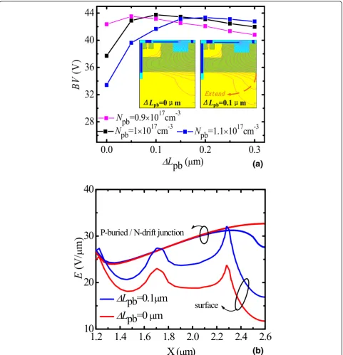
In order to achieve low Rd and high BV, partial
P-buried layer is introduced under the N-drift region.
Figure4a shows BV as a function ofΔLpbwith different Npb. For a given Npb, as ΔLpb increases, BV increases
and then decreases slightly. WhenΔLpb= 0.1μm, Npb=
1 × 1017cm−3, BV reaches the maximum value 43 V. The insert shows the equipotential contour profile with Npb
= 1 × 1017cm−3. It is indicated that the equipotential contour in the partial P-buried layer structure extends more to substrate with comparison to full P-buried layer.
(a)
(b)
Fig. 4aBV as a function ofΔLpbwith differentNpb. The insert is the equipotential contour profile withNpb= 1 × 10 17
[image:4.595.58.540.87.587.2]Figure4b shows electric field distribution at the surface and the P-buried/N-drift junction interface. For opti-mized conventional LDMOS, the breakdown occurs usu-ally at the N-drift/P-buried interface. For the proposed LDMOS, the junction of N-drift/P-sub replaces the junc-tion of N-drift/P-buried to relax the vertical electric field and extend depletion region, which results in a higher BV while maintaining lowRd.
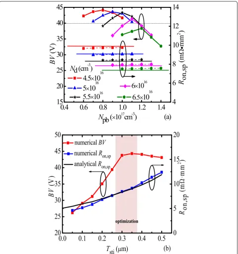
Charge balance between N-drift and partial P-buried layer is required to achieve high BV. Figure 5a shows that numerical and analytical BV and Ron,sp as functions
of the doping concentration of the P-buried (Npb) for
different Nd. For a given Nd, BV has a maximum value
with variedNpb, and the maximum ofBV increases with
the decrease of Nd. However,Ron,sp can be increased as
theNddecreasing. Due toBVrequired higher than 40 V, Fig. 5aNumerical (dotted line) and analytical (solid line) BV andRon,spas functions ofNpbfor differentNd.bNumerical (dotted line) and
analytical (solid line) BV andRon,spas functions ofTsti
[image:5.595.58.540.86.600.2]the Nd= 5.5 × 1016cm−3 and Npb= 1 × 1017cm−3 are
chosen. Figure 5b shows numerical and analytical BV and Ron,sp as functions of the thickness of the STI layer
(Tsti). Tsti has strong impact on BV and Ron,sp, and it
should be designed and optimized carefully as well as our previous work [21]. ForTsti< 0.3μm, the breakdown
point under the edge of poly field plate has a high elec-tric field peak. AsTstiincreases, the electric field peak is
relaxed, and then BV increases. For Tsti= 0.3μm, BV of
43 V is obtained. For Tsti≥0.3μm, the electric field peak
under the edge of poly field plate is enough low, as a re-sult, the breakdown point transfers to P/N junction under the drain side. AsTstiincreases, BV increases and
then saturates.
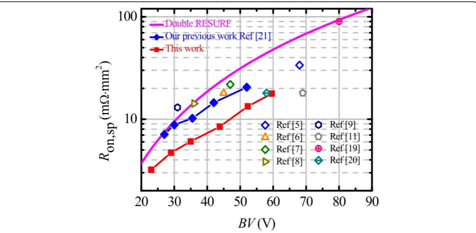
Figure 6 shows the benchmark of existing Bipolar-CMOS-DMOS (BCD) technologies and the proposed LDMOS. Apparently, the process technology for pro-posed LDMOS is compatible with our developed BCD technology which achieved the best-in-class performance of LDMOS. In the fabrication process for the proposed LDMOS, N-buried layer could share the same mask with P-well. For the proposed LDMOS,Ron,spis 8.5 mΩ·mm2
while BV = 43 V, which is reduced by about 37% com-pared with our previous work.
Conclusion
A novel ultra-low specific on-resistance LDMOS with enhanced dual-gate and partial P-buried layer is pro-posed and investigated by numerical simulation in this paper. N-buried layer with high doping concentration is utilized to achieve enhanced dual-gate with reducingRc.
Partial P-buried layer is introduced under the N-drift
region to enhance BV with keeping charge balance. The fabrication process of the LDMOS in this work is com-patible with the existing BCD technology reported in our previous work. The result shows that the Ron,sp of
the proposed LDMOS is reduced by 37% at BV of 43 V compared with previous work. With the semiconductor processing technology going to nanometer level, the
Ron,spcan reduce further with channel length decrease.
Abbreviations
BCD:Bipolar-CMOS-DMOS; BV: Breakdown voltage; LDMOS: Lateral double-diffused metal-oxide-semiconductor transistor; RESURF: Reduce surface-field;
Ron,sp: Specific on-resistance; USTI: Ultra-shallow trench isolation
Acknowledgements Not applicable.
Funding
This work was supported in part by the National Natural Science Foundation of China under Contract 61674027, in part by the China Postdoctoral Science Foundation Funded Project under Grant 2017 M612942, and in part by the Natural Science Foundation of Guangdong Province under Grant
2016A030311022 and 2018A030310015, in part by the Applied Fundamental Research Project of Sichuan Province under Grant 18YYJC0482, and in part by the Fundamental Research Funds for the Central Universities under Grant ZYGX2016J210.
Availability of Data and Materials
All data generated or analyzed during this study are included in this published article.
Authors’Contributions
ZW proposed the novel structure and was a major contributor in writing the manuscript. ZY built, deduced, and calculated the analytical model. XZ verified the analytical model by simulation software. Other authors offered comments and revised the manuscript. All authors read and approved the final manuscript.
Competing Interests
The authors declare that they have no competing interests.
[image:6.595.60.537.87.320.2]Publisher’s Note
Springer Nature remains neutral with regard to jurisdictional claims in published maps and institutional affiliations.
Received: 8 November 2018 Accepted: 14 January 2019
References
1. Disney D, Chan W, Lam R, Blattner R, Ma S, Seng W, Chen J-W, Cornell M, Williams R (2008) 60 V lateral trench MOSFET in 0.35μm technology. Proc ISPSD:24–27.https://doi.org/10.1109/ISPSD.2008.4538888
2. Erlbacher T, Bauer AJ, Frey L (2010) Reduced on resistance in LDMOS devices by integrating trench gates into planar technology. IEEE Electron Device Lett. 31(5):464–466.https://doi.org/10.1109/LED.2010.2043049 3. Shimamoto S, Yanagida Y, Shirakawa S, Miyakoshi K, Imai T, Oshima T,
Sakano J, Wada S (2011) High performance Pch-LDMOS transistors in wide range voltage from 35V to 200V SOI LDMOS platform technology. Proc ISPSD:44–47.https://doi.org/10.1109/ISPSD.2011.5890786
4. Fujii H, Tokumitsu S, Mori T, Yamashita T, Maruyama T, Maruyama T, Maruyama Y, Nishimoto S, Arie H, Kubi S, Ipposhi T (2017) A 90nm bulk BiCDMOS platform technology with 15–80V LD-MOSFETs for automotive applications. Proc ISPSD:73–76.https://doi.org/10.23919/ISPSD.2017.7988896. 5. Huang T-Y, Liao W-Y, Yang C-Y, Huang C-H, Yeh W-CV, Huang C-F, Lo K-H,
Chiu C-W, Kao T-C, Su H-D, Chang K-C (2014) 0.18 um BCD technology with best-in-class LDMOS from 6 V to 45 V. Proc ISPSD:179–181.https://doi.org/ 10.1109/ISPSD.2014.6856005
6. Lee K, Jeon H, Cho B, Cho J, Pang Y-S, Moon J, Kwon S, Hébert F, Lee J, Lee T (2013) 0.35μm, 30V fully isolated and low-Ron nLDMOS for DC-DC applications. Proc ISPSD:163–166.https://doi.org/10.1109/ISPSD.2013. 6694454
7. Jang J, Cho K-H, Jang D, Kim M, Yoon C, Park J, Oh H, Kim C, Ko H, Lee K, Yi S (2013) Interdigitated LDMOS. Proc ISPSD:245–248.https://doi.org/10.1109/ ISPSD.2013.6694462.
8. Roggero R, Croce G, Gattari P, Castellana E, Molfese A, Marchesi G, Atzeni L, Buran C, Paleari A, Ballarin G, Manzini S, Alagi F, Pizzo G (2013) BCD8sP: an advanced 0.16μm technology platform with state of the art power devices. Proc ISPSD:361–364.https://doi.org/10.1109/ISPSD.2013.669442.
9. Ko K-S, Lee S-H, Kim D-H, Eum J-N, Park S-K, Cho I-W, Kim J-H, Yoo K-D (2013) HB1340 - advanced 0.13 um BCDMOS technology of complimentary LDMOS including fully isolated transistors. Proc ISPSD:159–162.https://doi. org/10.1109/ISPSD.2013.6694453.
10. van der Pol JA, Ludikhuize AW, Huizing HGA, vanVelzen B, Hueting RJE, Mom JF, van Lijnschoten G, Hessels GJJ, Hooghoudt EF, van Huizen R, Swanenberg MJ, Egbers JHHA, van den Elshout F, Koning JJ, Schligtenhorst H, Soeteman J (2000) A-BCD: an economic 100 V RESURF silicon-on-insulator BCD technology for consumer and automotive applications. Proc ISPSD:327–330.https://doi.org/10.1109/ISPSD.2000.856836
11. Wei J, Luo X, Ma D, Wu J, Li Z, Zhang B (2016) Accumulation mode triple gate SOI LDMOS with ultralow on-resistance and enhanced
transconductance. Proc ISPSD:171–174.https://doi.org/10.1109/ISPSD.2016. 7520805
12. Ge W, Luo X, Wu J, Lv M, Wei J, Ma D, Deng G, Cui W, Yang YH, Zhu KF (2017) Ultra-low on-resistance LDMOS with multi-plane electron accumulation layers. IEEE Electron Device Lett. 38(7):910–913.https://doi. org/10.1109/LED.2017.2701354
13. Guo Y, Yao J, Zhang B, Lin H, Zhang C (2015) Variation of lateral width technique in SOI high-voltage lateral double-diffused metal–oxide– semiconductor transistors using high-k dielectric. IEEE Electron Device Lett. 36(3):262–264.https://doi.org/10.1109/LED.2015.2393913
14. Duan B, Yang Y, Zhang B (2009) New superjunction LDMOS with N-type charges’compensation layer. IEEE Electron Device Lett 30(3):305–307. https://doi.org/10.1109/LED.2009.2012396
15. Fujishima N, Sugi A, Kajiwara S, Matsubara K, Nagayasu Y, Salama CAT (2002) A high-density low on-resistance trench lateral power MOSFET with a trench bottom source contact. IEEE Trans. Electron Devices 49(8):1462–1468. https://doi.org/10.1109/TED.2002.801434
16. Xia C, Cheng X, Wang Z, Xu D, Cao D, Zheng L, Shen L, Yu Y, Shen D (2014) Improvement of SOI trench LDMOS performance with double vertical metal field plate. IEEE Trans Electron Devices 61(10):3477–3482.https://doi.org/10. 1109/TED.2014.2349553
17. Iqbal MM-H, Udrea F, Napoli E (2009) On the static performance of the RESURF LDMOSFETS for power ICs. Proc ISPSD:247–250.https://doi.org/10. 1109/ISPSD.2009.5158048.
18. Yoo A, Ng JCW, Sin JKO, Ng WT (2010) High performance CMOS-compatible super-junction FINFETs for sub-100 V applications. IEDM Tech Dig:20.7.1–20. 7.4.https://doi.org/10.1109/IEDM.2010.5703402
19. Nitta T, Yanagi S, Miyajima T, Furuya K, Otsu Y, Onoda H, Hatasako K (2006) Wide voltage power device implementation in 0.25μm SOI BiC-DMOS. Proc ISPSD:1–4.https://doi.org/10.1109/ISPSD.2006.1666141
20. Yamaguchi H, Urakami Y, Sakakibara J (2006) Breakthrough of on-resistance Si limit by super 3D MOSFET under 100 V breakdown voltage. Proc ISPSD:1– 4.https://doi.org/10.1109/ISPSD.2006.1666071
21. Jin F, Liu D, Xing J, Yang X, Yang J, Qian W, Yue W, Wang P, Qiao M, Zhang B (2017) Best-in-class LDMOS with ultra-shallow trench isolation and p-buried layer from 18V to 40V in 0.18μm BCD technology. Proc ISPSD:295– 298.https://doi.org/10.23919/ISPSD.2017.7988962