© 2017, IRJET | Impact Factor value: 5.181 | ISO 9001:2008 Certified Journal | Page 3269
LOW POWER LOGIC CIRCUIT BASED ADIABATIC LOGIC USING VTCMOS
Poongodi.M
1, Jeyashri.M
2, Muthusuriya.M
3, Thiruppathiraja.M
4123
PG Scholar, Department of ECE, Theni Kammavar Sangam college of Technology, Tamilnadu, India.
4
Assistant Professor,
Department of ECE, Theni Kammavar Sangam college of Technology, Tamilnadu, India.
---***---Abstract -
Adiabatic Logic is the term given to low-power electronic circuits that implement reversible logic. The term comes from the fact that an adiabatic process is one in which the total heat or energy in the system remains constant. Research in this area has mainly been fueled by the fact that as circuits get smaller and faster, their energy dissipation greatly increases a problem that an adiabatic circuit promises to solves. Most research has focused on building adiabatic logic out of CMOS. However, current CMOS technology, though fairly energy efficient compared to similar technologies, dissipate energy as heat, mostly when switching. Two logic families i.e. CMOS logic and adiabatic logic have been analyzed and implemented. The simulation was conducted in Tanner EDA. Finally the power consumption is estimated and compared.Key Words
: Adiabatic logic, Carry looks ahead adder (CLA), low power, leakage, CMOS, substrate biasing.1. INTRODUCTION
The demand for implementing ultralow power digital systems in many modern application, such as mobile systems, sensor networks and implanted biomedical systems, has increased the importance of designing logic circuits in subthreshold regime. These emerging applications have low energy as the primary concern instead of performance, with the eventual goal of harvesting energy from the environment. In subthreshold logic [2]-[4], circuits
operate with a supply voltage VDD lower than the transistor
threshold voltage VT and utilize the subthreshold leakage
current as the operating current. Conventional CMOS logic circuits utilizing subthreshold transistors can typically operate with a very low power consumption[9], which is mainly due to the dynamic power consumption and is
quadratically dependent upon the supply voltage as CL f V 2
DD (where CL , f and VDD are the load capacitance, operating
frequency and the supply voltage, respectively).
Recently, adiabatic logic (or energy recovery logic) [5]–[7] style has emerged as a promising approach in strong inversion regime, to reduce dynamic power consumption significantly without sacrificing noise immunity and driving ability. These circuits achieve ultralow energy consumption by steering currents across devices with low voltage differences and by gradually recycling the energy stored in their capacitive loads, especially in low-frequency regime. Since the performance requirements are quite relaxed in many of these energy- efficient sub threshold applications
[2], [4], we believe that the adiabatic style can be used efficaciously in a sub threshold regime to make the circuit more energy efficient.
In general, the design of adiabatic logic requires a deep knowledge of the main features of the adopted logic style, such as power dissipation, leakage current impact of temperature variation, operating frequency, and noise immunity. In this paper, the behaviors of adiabatic logic in sub threshold regime are discussed in depth. To demonstrate the workability of the adiabatic logic circuits in sub threshold regime, a 4-bit carry look ahead adder (CLA) unit is adopted as a reference circuit.
2. SUBTHRESHOLD ADIABATIC LOGIC
2.1 Basic Model of MOSFET in Sub threshold
Regime
Using EKV model [8], the I–V characteristics of the sub
threshold pMOS device can be expressed by
(1)
Where I0 = 2η p μ p Cox(W /L )VT2. VSG, VSD, and VTH are source
to gate, source to drain, and threshold voltage of pMOS,
respectively. VT = (k T /q) is thermal voltage, η p is sub
threshold slope factor, and μp is the mobility of pMOS device.
In sub threshold regime, the threshold voltage (VTH) depends
on source-to-drain voltage (VSD) through body effect and
drain-induced barrier lowering. Considering these effects,
threshold voltage can be expressed as follows:
VTH=VT0-γVSB-ηVSD. (2)
Here,VTO is the threshold voltage at zero bias and γ and η are
the body effect and drain-induced barrier lowering coefficient, respectively. The Drain Induced Barrier Lowering coefficient (η) [8], which is a unit less quantity, can be expressed as
η = 1/ (2 cosh (Leff/2lt)) (3)
Where lt = (εSi Tox X Dep/β εox)1/2 and
γ=√(2q€siNA/Cox) (4)
© 2017, IRJET | Impact Factor value: 5.181 | ISO 9001:2008 Certified Journal | Page 3270
(5)
Where KP=I0 exp (−VTO−ηVSD/nPVT). For the sake of
simplicity, let us further simplify the magnitude of Kp by
assuming, ηVSD/npVT ≪ 1.The value of η can be obtained
directly from the 45- nm PTM model file. Putting the model parameters in (3) and (4), η will be slightly less, approximately 0.0039. Hence, we set, η→0.004for pMOS
and nMOS both, thermal voltage, VT=26mVat27°C, np=1.62,
VSD lies in the range of few milli volts to hundreds of milli
volts depending on the VSG of the pMOS device. In the case
of a pMOS device, we get KP≈I0 exp (−VTO/nPVT). Kp and
Kn Differ due to imbalance in zero biased threshold
voltage(VTO), mobility(µ), sub threshold swing(n) ,and
soon. In45-nm technology, as I0 for pMOS and nMOS are
1.16 and 0.55µA, respectively, Kpand Kn will be obtained
by putting the value from PTM 45-nm metal gate/high-K
model file [11]. Hence, KP∼1.25 and Kn∼8.79pA .By
changing (W/L) ratio, we can also tune Kp or Kn as these
are directly proportional to the aspect ratio of transistors.
2.2 Behavior of MOSFET under ac Supply
Voltage in Sub threshold Regime
In adiabatic logic circuits, ramp type supply voltage is used to slow down the charge transport mechanism [5], [10].
Fig. 1. (a) Clock supply voltage. (b) Equivalent circuit of
pMOS under low and high VSD. (c) SAL inverter circuit. (d)
SAL inverter symbol.
Hence, the supply clock plays the pivotal role. A ramp type
supply voltage φ(t) is considered in Fig. 1(a), which
gradually swings in between logic0 (Gnd potential) and logic1
(VDD) in time duration 2T, where f (=1/2T) is the supply
clock’s frequency. The power supply waveform φ(t) can be
divided into charging phase, when φ(t) ramps up from 0 to
VDD in 0 to T unit time and discharging phase when φ(t)
ramps down from VDD to 0 in T to 2T unit time. Considering
the charging phase, the voltage at any time instant can be expressed as
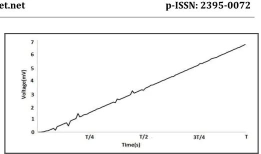
[image:2.595.305.567.66.220.2]φ(
t) = VDD(t/T) (6)Fig.2. Variation of V with respect to time.
2.3 Impact of Parasitic Gate Capacitances on
Variable Supply Voltage
In a sub threshold digital CMOS circuit, the gate capacitance of the transistor varies if the supply voltage ramps up (charging phase) or down (discharging phase). Due to this, a negligible amount of energy is transferred from variable supply voltage to the inputs, causing an on adiabatic loss. This non adiabatic loss of energy also brings noise or some unwanted spikes in output node voltages. Since during adiabatic switching, MOSFETs are kept under low drain to
source voltages, the total gate capacitance (CG) of a pMOS
device can be expressed as
CG=CGD+CGS (7)
Where CGD and CGS are the gate to drain and gate to source
capacitances, respectively. If can be assumed that initially the gate voltage and supply voltages are at zero potential. When the supply voltage ramps up, within a short time span, the gate voltage rises gradually from 0 to VDD. As a result, the
total CGVDD amount of charge flows to the gate node, causing a
0.5 CG(VDD)2 J of energy loss. When the supply voltage reaches
the peak of VDD, the drain to gate voltage (VDG) and the source
to gate voltage (VSG) become zero, causing a current flow
from the gate node to the input line. The nergy associated
during this event is CGVDD2. As a result, a 0.5 CG(VDD)2 energy
flows from the gate node to the input.
2.4 Impact of Leakage for Variable Supply Voltage
As leakage current is one of the pivotal concerns in sub threshold regime, total leakage energy dissipations in SAL along with the conventional one are given. Hence, leakage current is assumed to flow through the pMOS device for higher drain to source voltage drop. Under this condition, forthe half clock period of supply voltage, ϕ(t), the total leakage
energy Dissipation Across a pMOS can be expressed as
= (8)
Assuming VDD/npVT >>1, we get
[image:2.595.41.294.434.589.2]© 2017, IRJET | Impact Factor value: 5.181 | ISO 9001:2008 Certified Journal | Page 3271 Considering the constant dc supply voltage having the same
value as the peak of 𝜙(t), the total leakage across a pMOS device can be expressed as
E leak,conv=VDDTKp (10)
2.5 Delay Calculation
As SAL is efficacious where instead of performance, power dissipation is major concern. For example, in implanted biomedical systems, the circuits remain active for a very small span of time and remain idle for most of the time. In such operations, much lower frequency ranges are required. Therefore, in SAL, minimization of power dissipation is the pivotal issue. Hence, we address the delay in SAL though it would be few times larger than that in the conventional one. In SAL-based digital circuits, output nodes follow the supply clock very closely during the charging and discharging periods and the output waveforms get the same pattern as the supply voltage. In general, delay can be calculated
between a change in an input (50% of VDD on input) and a
low-to-high or high-to-low change in the output (50% of VDD
on input). As the supply voltage ramps up and down linearly
in between 0 and VDD, propagation delay would be roughly T
/2, where 2T is the width of total supply clock. In the worst
case corner, SS and worst temperature 80 °C less than 1%
variation in delay is observed where the time period is 10 μs.
Therefore, in worst case process variation of chip and die, delay would not be affected significantly. A 3% relative delay variation has been observed with three sigma variation on the path. Though process variations do not affect the propagation delay of SAL, increasing the frequencies can minimize the propagation delay. Increasing supply voltage also enhances the speed a bit. Simultaneously, power dissipation must increase with speed. However, we should keep in mind that minimizing power dissipations would be
more important than decreasing the delay in SAL.
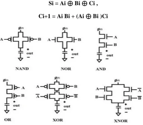
3. Subthreahold Adiabatic logic based 4 bit CLA
In this section, design and analysis of SAL-based 4-bit CLA are given to show the workability and the feasibility of the proposed logics. After verifying the logical functionality, we implemented an SAL-based standard cell library, consisting of common digital gates, such as buffer/inverter, two-input and three-input functions, complex gates, and special gates like half and full adder, which are necessary to implement the 4-bit CLA. For example, to implement a NAND or a NOR gate, simply the pull-up network can be placed between the supply clock and the output load capacitors, whereas an AND or an OR gate can be implemented using the pull-down network between the supply clock and the output load capacitors. In case of a NAND structure, for every input
combination except A = B = 1, the output node voltage will
follow the supply clock closely, and we get a triangular
output waveform. When A = B = 1 through parallel pMOS
transistor, leakage currents will flow as the transistors will behave almost as a constant current source. A very small
amount of charge will be stored across the load capacitor, i.e., instead of ground potential, very small voltage will be dropped across the output.
Hence, we implemented the sum (Si) in three stages to avoid
delay mismatching with the carry generation. In SAL-based 4-bit CLA, every stage will be controlled by the supply clock.
Like the conventional approach, the expression of the i th
sum and the (i+1) th carry output can be given as
Si = Ai ⊕ Bi ⊕ Ci ,
Ci+1 = Ai Bi + (Ai ⊕ Bi )Ci
Fig 3. Logical structure of basic SAL logic gate.
[image:3.595.310.552.204.414.2] [image:3.595.329.568.459.655.2]© 2017, IRJET | Impact Factor value: 5.181 | ISO 9001:2008 Certified Journal | Page 3272
4. Simulation Results
4.1 Layout of 4 Bit SAL based CLA
4.2 Output
0.0 0.1 0.2 0.3 0.4 0.5 0.6 0.7 0.8 0.9 1.0 Time (us) 0.0 1.0 2.0 3.0 4.0 5.0 V o l ta g e ( V ) v(a0) Cell0
0.0 0.1 0.2 0.3 0.4 0.5 0.6 0.7 0.8 0.9 1.0 Time (us) 0.5 1.0 1.5 2.0 V o l ta g e ( V ) v(3) Cell0
0.0 0.1 0.2 0.3 0.4 0.5 0.6 0.7 0.8 0.9 1.0 Time (us) 0.0 1.0 1.5 2.5 3.0 4.0 4.5 V o l ta g e ( V ) v(s0) Cell0
0.0 0.1 0.2 0.3 0.4 0.5 0.6 0.7 0.8 0.9 1.0 Time (us) 0.0 1.0 1.5 2.5 3.0 4.0 4.5 V o lt a g e ( V ) v(s1) Cell0
0.0 0.1 0.2 0.3 0.4 0.5 0.6 0.7 0.8 0.9 1.0 Time (us) 0.5 1.5 2.5 3.5 V o lt a g e ( V ) v(cr1) Cell0
0.0 0.1 0.2 0.3 0.4 0.5 0.6 0.7 0.8 0.9 1.0 Time (us) 0.5 1.5 2.5 3.5 V o lt a g e ( V ) v(cr0) Cell0
0.0 0.1 0.2 0.3 0.4 0.5 0.6 0.7 0.8 0.9 1.0 Time (us) 0.5 1.0 1.5 2.0 2.5 V o lt a g e ( V ) v(4) Cell0
0.0 0.1 0.2 0.3 0.4 0.5 0.6 0.7 0.8 0.9 1.0 Time (us) 0.0 1.0 2.0 3.0 4.0 5.0 V o lt a g e ( V ) v(b0) Cell0
0.0 0.1 0.2 0.3 0.4 0.5 0.6 0.7 0.8 0.9 1.0 Time (us) 0.0 1.0 2.0 3.0 4.0 5.0 V o l t a g e ( V ) v(c0) Cell0
4.3 Comparision table
S.NO Gates Name CMOS Logic (in Watts) Adiabatic Logic (in Watts)
1 AND
Gate
5.537651e-004 4.709910e-004
2 OR Gate 1.216141e-003 9.671850e-008
3 NAND
Gate
2.087821e-004 8.292000e-008
4 NOR
Gate
2.243673e-004 1.341909e-006
5 XOR
Gate
1.734818e-003 6.853403e-004
6 XNOR
Gate
2.430037e-003 1.124347e-003
7 Half
Adder
3.084999e-003 1.375516e-003
8 Full
Adder
9.031094e-003 2.463585e-003
9 D Flip
Flop
4.798298e-003 1.267636e-004
10 4 bit
CLA
1.223646e-001 3.493855e-002
5. CONCLUSIONS
© 2017, IRJET | Impact Factor value: 5.181 | ISO 9001:2008 Certified Journal | Page 3273
6. Future work
6.1 Variable Threshold CMOS (VTCMOS)
One of the efficient methods to reduce power consumption is to use low supply voltage and low threshold voltage without losing speed performance. But increase in the lower threshold voltage devices leads to increased sub threshold leakage and hence more standby power consumption. Variable Threshold CMOS (VTCMOS) devices are one solution to this problem. In VTCMOS technique threshold voltage of the low threshold devices are varied by applying variable substrate bias voltage from a control circuitry.
VTCMOS technique is very effective technique to reduce the power consumption with some drawbacks with respect to manufacturing of these devices. VTCMOS requires either twin well or triple well technology to achieve different substrate bias voltage levels at different parts of the IC. The area overhead of the substrate bias control circuitry is negligible. It will completely to remove the negative feedback voltage within the circuit. The negative feedback voltage will get dissipated through ground
REFERENCES
[1] Manash Chanda, Sankalp Jain, “Implementation of
subthreshold adiabatic logic for ultra low power application” Chandan Kumar Sarkar, Senior Member, IEEE.2015.
[2] T.-T. Liu and J. M. Rabaey, “A 0.25 V 460 nW
asynchronous neural signal processor with inherent
leakage suppression,” IEEE J. Solid-State Circuits, vol. 48,
no. 4, pp. 897–906, Apr. 2013.
[3] Calimera, A. Macii, E. Macii, and M. Poncino, “Design
techniques and architectures for low-leakage SRAMs,”
IEEE Trans. Circuits Syst. I, Reg. Papers, vol. 59, no. 9, pp. 1992–2007, Sep. 2012.
[4] J. Kwong, Y. K. Ramadass, N. Verma, and A. P.
Chandrakasan, “A 65 nm sub-Vt microcontroller with
integrated SRAM and switched capacitor DC-DC
converter,” IEEE J. Solid-State Circuits, vol. 44, no. 1, pp.
115–126, Jan. 2009.
[5] C.-S. A. Gong, M.-T. Shiue, C.-T. Hong, and K.-W. Yao,
“Analysis and design of an efficient irreversible energy
recovery logic in 0.18-μm CMOS,” IEEE Trans. Circuits
Syst. I, Reg. Papers, vol. 55, no. 9, pp. 2595–2607, Oct. 2008.
[6] N. S. S. Reddy, M. Satyam, and K. L. Kishore, “Cascadable
adiabatic logic circuits for low-power applications,” IET
Circuits, Devices Syst.,vol. 2, no. 6, pp. 518–526, Dec. 2008.
[7] V. S. Sathe, J.-Y. Chueh, and M. C. Papaefthymiou,
“Energy-efficient GHz-class charge-recovery logic,” IEEE
J. Solid-State Circuits, vol. 42, no. 1, pp. 38–47, Jan. 2007.
[8] Y. Tsividis, Operation and Modeling of the Transistor
MOS, 2nd ed.Oxford, U.K.: Oxford Univ. Press, 2003.
[9] H. Soeleman, K. Roy, and B. C. Paul, “Robust sub
threshold logic for ultra-low power operation,” IEEE
Trans. Very Large Scale Integr. (VLSI) Syst., vol. 9, no. 1, pp. 90–99, Feb. 2001.
[10] D. Maksimovic, V. G. Oklobdzija, B. Nikolic, and K. W.
Current, “Clocked CMOS adiabatic logic with integrated
single-phase power clock supply,” IEEE Trans. Very