AN INTERLEAVED HIGH GAIN BOOST CONVERTER WITH SVM
INVERTER FOR A MOTOR LOAD USING PV PANELS
P. Deepak and A. Ramesh Babu
Department of Electrical and Electronics Engineering, Sathyabama University, Chennai, India
E-Mail:[email protected]
ABSTRACT
The Interleaved High voltage gain boost converter along with SVM inverter is proposed to power induction motor using PV panels. The high voltage gain of interleaved boost converter is obtained through asymmetrical PWM, voltage lift capacitor. The ILBC reduces the voltage stress of main switch and reduce the input current ripple. The output of PV panel is fed to the input of ILBC. The boost converter output voltage is supplied to SVM inverter, which provides the power to induction motor. The SVM inverter provides the increased fundamental output voltage; reduce the harmonic content and Torque. Simulation was carried out using MATLAB/simulink environment. The comparison of SVM inverter and PWM inverter was made to validate the proposed converter.
Keywords: interleaved boost converter, PV panel, SVM inverter, THD.
INTRODUCTION
Rapid deployment of renewable energy and energy efficiency is resulting in significant energy security, climate change mitigation, and economic benefits. In international public opinion surveys there is strong support for promoting renewable sources such as solar power and wind power. At the national level, at least 30 nations around the world already have renewable energy contributing more than 20 percent of energy supply. One of today’s fastest growing renewable energy technologies is Photovoltaic PV power systems. Converting sunlight into electricity, solar power is used in two ways, one is direct using PV and another one is indirectly using concentrated solar power. Lenses or mirrors and tracking systems are used in CSP in order to get more sunlight into a beam which is smaller one. Photovoltaic module is a number of solar cells connected electrically to each other and mounted a frame which is designed to produce current at certain levels.
Solar energy is more environmental-friendly and higher in mobility than that of hydroelectricity and geothermal energy. The transformer less photovoltaic (PV) power system has been created an impact for its lower cost, smaller volume, and higher efficiency, compared with transformer based PV power system. To achieve output voltage greater than its input voltage a converter is used called Boost converter or step-up converter. Batteries, solar panels, rectifiers and DC generators are the input sources for the boost converter. The space vector pulse
Width modulation (SVPWM) technique is most widely used for efficient operation of Induction motor. SVPWM provides more efficient use of supply voltage which means it increases fundamental output without distorting line to line waveform and the harmonic content generated will be less when compared with other
modulation technique. The proposed topology aims to reduce the input current ripple and low output harmonics thus increasing the converter efficiency and precise control system.
LITERATURE REVIEW
modulation techniques are analysed to find out the reduction of harmonics at the output [12]. The combination ILBC and SVPWM inverter is proposed for powering an induction motors with the solar panel as the source will be more useful for the irrigation purposes and remote locations were the availability of conventional power is less.
Table-1.Simulation specifications.
1 Switching frequency(f) 25khz
2 Input voltage (Vin) 40V
3 Output voltage (Vo) 400V
4 Output power (P) 500W
5 Input inductance (L1 and L2) 100µH
6 Output Capacitance (C1 and C2) 40µF and 100µF
7 Switches (S1 and S2) IRFB4710 MOSFET
8 Diodes (D1 and D2) MBR
10200
Block diagram
Figure-1. Proposed block diagram.
Proposed block diagram, as shown in Figure-1. In this proposed system consist of solar panel, Interleaved Boost Converter, SVM inverter and PI controller. The solar panel output voltage is increased by the use of boost converter. This interleaved boost converter provides high voltage gain and reduces the current ripple. The stepped-up voltage is fed to SVM inverter which powers the induction motor with reduced harmonics. The speed of induction motor controlled with help of PI controller with reference one. The Ziegler Nicholas method is used to find gain values of proportional and integral controller.
Circuit diagram
Proposed circuit diagram, is shown in Figure-2.The input voltage is obtained from solar panel fed input of interleaved boost converter.
The interleaved boost converter consist of boost inductor L1 and L2, MOSFET switches S1 and S2, Diodes D1 and D2 with lift capacitor Cb. The switches are turn on by switching frequency of 25Khz with 180o phase shift.
The SVM inverter drawn voltage from boost converter. The output of SVM inverter is fed to stator of three phase induction motor.
Figure-2.Proposed circuit diagram.
PV modelling
Figure-3.PV modelling diagram.
Solar panel has been designed in MATLAB and it act as a only source for the entire proposed circuit. The solar panel generates a voltage of around 40V which is given as the input to the interleaved boost converter (ILBC) for boosting the voltage.
Space vector modulation (SVM)
In SVM, the inverter was considered as a single unit with eight unique states. The sinusoidal voltage was treated with constant amplitude (V) and rotating at constant frequency (F).
This technique is applied by sampling the reference voltage Vref with eight switching pattern combinations. For a three leg switching pattern and two possible states, we can get eight possible combinations as
1 Out1
40.63
Vpv Product
197.1 Ppv
Ipv Insolation
Vpv Ppv
PV module (I)
PV1
4.85 PV current 1000
Insolation
Add Ppv
six non zero state vectors (V1 to V6) and two zero state vectors (V0 and V7). Finally to implement Space vector modulation technique, the transformation has to be coordinated from a-b-c reference frame to stationary d-q reference frame.
Then it involves vectorially decomposing a desired voltage space vector V into voltage vector components that can be generated using a typical three-phase inverter.
The vectors (V1 to V6) of the plane was divided equally in to six sectors of each displaced by 60 degree. Vref is generated by two adjacent non-zero vectors and two zero vectors.
The ON-OFF states of both upper leg and lower leg are opposite to each other.
Modulation algorithm with MATLAB
Step-1: To read the three phase reference voltages as(Va, VbandVc)
Figure-4.Generation of three phase sinusoidal waveform.
From the above Figure-3 shows three sine waves are generated as Va,Vb and Vc at an amplitude of 1. These three signals are electrically 120o apart from each other.
Figure-5.Over all SVPWM block.
The above SVPWM block calculates the magnitude and direction of reference voltage Vref, the
sector which it lies between (1 to 6), Time duration Tx,Ty and T0 and Switching time of each transistor(Ta1,Tb1,Tc1,Ta2,Tb2and Tc2).
Step-2: To transform rotational three phase quantity to stationary two phase quantities (a,b,c to d,q). The rotational three phase quantity Va,Vb,Vc was transformed to stationary direct and quadrature axis Vd and Vq.
Step-3: To calculate the Voltage of direct axis Vd, Voltage of quadrature axis Vq and arc tangent angle.
cn bn an q dV
V
V
2
3
2
3
0
2
1
2
1
1
3
2
V
V
cn bn an cn bn q cn bn an cn bn an dV
2
3
V
2
3
V
cos30
V
cos30
V
0
V
V
2
1
V
2
1
V
cos60
V
cos60
V
V
V
The stationary two phase quantity named as Vd and Vq. From the Vd and Vq Magnitude and direction of the reference voltage are calculated. The calculated magnitude and angle was taken for determining the time duration Tx,Ty and T0.
Figure-6.α angle andsector calculation.
Step-4: To calculate the reference voltage Vref and the sector in which it lies.
t
2
ππ
t
ω
)
V
V
(
tan
α
V
V
V
s s q 1 2 q 2 d ref
1 3phFrom the Figure-5 and above equation the angle α
and sector was identified. The angle between Vd and Vq was calculated and given to the timing block to select the time duration for the corresponding vector.
Step-5: According to the sector identified the corresponding switching vectors are to be identified.
Step-6: To calculate the switching time
[image:4.612.335.531.114.244.2]according to the output voltage vector magnitude.
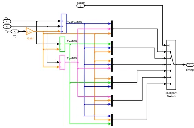
Figure-7.Tx, Ty and T0 calculation.
From the above figure and the below equation the time duration of Tx, Ty and T0 for any sector was calculated. The calculated Tx,Ty,T0 are given as the input to timing block where the Tx,Ty,T0 are combined according to the sector. By combining Tx, Ty and T0 the Switching time of all MOSFET was calculated for each sector. 60 α 0 6) to Sector1 is, (that 6 through 1 n where, , 3 1 cos sin 3 1 sin cos 3 3 1 sin 3 sin 3 cos cos 3 sin 3 3 sin 3 3 1 3 sin 3
0 T Tx Ty
[image:4.612.76.291.227.367.2]T n n V ref V T n V ref V T Ty n n V ref V T n V ref V T n V ref V T Tx dc z dc z dc z dc z dc z
Figure-8.Tx,Ty and T0 combination.
From the above figure the Tx, Ty and T0 are combined to determine the switching time duration of each MOSFET
Step-7: To determine the switching sequence as per the Table-1.
Step-8: Control signals are to be sent to gate terminal of each switching device.
Step-9: To calculate the output voltage across the load terminals.
Space vector switching
A three phase inverter consist of three half bridges. Hence eight switching states are produced six of them are non zero vectors while two are zero vectors. The zero vectors are produced when the bridge is completely closed (V7) or open (V0) i.e. all upper or all lower legs are
conducting simultaneously.
Since the upper switches decides the output voltages, all analysis can be based on the three switching sequence at the bases of the three upper MOSFET switches. Then there will be 23=8, permissible switching
states (000, 001, 010, 011, 100, 101, 110, 111). The table gives summary of the switching states and corresponding conduction states of the IGBTs. Each state contributes a three-phase voltage output which will be one space voltage vector. There will be eight space voltage vectors for eight switching sequence. But 000 state is vector Vo,
001 state will be V5, 010 will be V3 and so on. The space
voltage vector and corresponding states are shown in the table. From the Table, it can be seen that V1, V2, V3, etc.,
[image:4.612.72.270.492.668.2]Table-1.
Space voltage
vector
State
Conduction of Mosfets
ON OFF
V0 0 0 0 Tc2, Ta2, Tb2 Ta1, Tb1, Tc1
V1 1 0 0 Ta1, Ta2, Tb2 Tb1, Tc2, Tc1
V2 0 1 1 Ta1, Tb1, Tb2 Tc1, Tc2, Ta2
V3 0 1 0 Tc2, Tb1, Tb2 Ta1, Tc1, Ta2
V4 1 1 0 Tc2, Tb1, Tc1 Ta1, Ta2, Tb2
V5 1 0 0 Tc2, Ta2, Tc1 Ta1, Tb1, Tb2
V6 1 0 1 Ta1, Ta2, Tc1 Tc2, Tb1, Tb2
V7 1 1 1 Ta1, Tb1, Tc1 Tc2, Ta2, Tb2
RESULTS AND DISCUSSIONS
Figure-9.Solar panel output voltage.
From the above figure we can see the output voltage from the solar panel of around 40Volts at 4.5Amps generated at irradiation of 1000W/m2.
Figure-10.Boosted output voltage from interleaved boost converter versus time.
From the above figure the output voltage from the interleaved boost converter is 400Volts.The boost converters have voltage gain of 10.
Figure-11.Motor speed versus time.
From the above figure the motor speed rises and reaches 1548rpm and remains there as constant speed throughout.
Figure-12. Phase to phase voltage.
From the above figure the line to line voltage is around 400V AC which is symmetrical in nature.
Figure-14. Gate pulses of LOWER arm MOSFET.
From the above figure the gate pulses are shown for all three lower arm MOSFET’s.
Figure-15.Motor torque versus time.
From the above Figure the Torque value raises and settles at 1.66 NM.
Figure-16.Total harmonic distortion for SVM.
From the above Figure it is clear that the THD is 5.31% only.
Comparison between PWM inverter and SVM inverter
S.No. Parameters PWMinver
ter
SVM inverter
1 Output Voltage 250V(L-L) with ripple 400V(L-L)
2 THDi 20% 5.31%
3 Speed with ripple 1492 rpm 1548 rpm, steady speed
4 Torque with ripple 5.18 NM 1.66 NM
5 Power factor 0.4 0.6
CONCLUSIONS
The ILBC-SVM inverter system is designed modelled and simulated using MATLAB. ILBC is proposed to increase the life of PV panel and power rating of converter. SVM inverter is proposed to reduce the heating of motor and improve its life. The simulation results with motor are presented. Thus the harmonics are reduced by using SVM inverter.
REFERENCES
[1] Fernando LessaTofoli,Demercil de souzaoliveria,Jr. Rene pastor Torrico-Bascopeand yblinjaneth Acosta Alcazar. 2012. Novel non isolated high voltage gain Dc-Dc converters based on 3SSC and VMC. IEEE Transaction on power electronics. 27(9).
[2] Yohan park and sewanchoi. Soft switched Interleaved Boost converters for high step up and High power applications. 978-1-4244-5395-/10/$26.00@2010IEEE.
[3] Kuo-Ching Tseng, Chi-Chih Huang and Wei-Yuan Shih. 2013. A High Step-Up Converter with a Voltage Multiplier Module for a Photovoltaic System.IEEE transactions on power electronics. 28(6).
[5] W. Li and X. He. 2007. An interleaved windingcoupledboost converter with passivelossless clamp circuits. IEEE Trans. Power Electron. 22(4): 1499-1507.
[6] Arundathi Ravi, A.RameshBabu. 2014. Non-isolated Three Stage Interleaved Boost Converter for High Voltage Gain. International Journal of Scientific and Technology Research. 3(3).
[7] Gustavo A. L. Henn, R. N. A. L. Silva, Paulo P. Prac¸a, Luiz H. S. C. Barreto, Member, IEEE and Demercil S. Oliveira Jr. 2010. Interleaved-Boost Converter with High Voltage Gain. IEEE Transactions on power electronics. 25(11).
[8] Yufei Zhou, Student Member, IEEE, Wenxin Huang, Member, IEEE, Ping Zhao and Jianwu Zhao A Transformerless Grid-Connected Photovoltaic System Based on the Coupled Inductor Single-Stage Boost Three-Phase Inverter.
[9] Tan KhengSuan Freddy, Nasrudin A. Rahim, Senior Member, IEEE, Wooi-Ping Hew, Member, IEEEand Hang SengChe. 2014. Comparison and Analysis of Single-Phase Transformerless Grid-Connected PV Inverters. IEEE transactions on power electronics. 29(10).
[10]R. Gonzalez, J. Lopez, P. Sanchis and L. Marroyo. 2007. Transformerless inverter for single-phase photovoltaic systems.IEEE Trans. Power Electron. 22(2): 693-697.
[11]S. V Araujo, P. Zacharias and R. Mallwitz. 2010. High efficiency single-phase transformerless inverters for grid-connected photovoltaic systems. IEEE Trans. Ind. Electron. 57(9): 3118-3128.
[12]M. C. Cavalcanti, K. C. de Oliveira, A. M. de Farias, F. A. S. Neves, G. M. S. Azevedo and F. Camboim. 2010. Modulation techniques to eliminate leakage currents in transformerless three-phase photovoltaic systems. IEEE Trans. Ind. Electron. 579(4): 1360-1368.
[13]O. Lopez, F. D. Freijedo, A. G. Yepes, P. Fernandez-Comesana, J. Malvar,R. Teodorescu and J. Doval-Gandoy. 2010. Eliminating ground current in a transformerless photovoltaic application.IEEE Trans. Energy Convers. 25(1): 140-147.
[14]B. Gu, J. Dominic, J.-S. Lai, C.-L. Chen, T. LaBella and B. Chen. 2013. High reliability and efficiency single-phase transformerless inverter for gridconnected photovoltaic systems.IEEE Trans. Power Electron. 28(5): 2235-2245.