Characterization of PNN Stack SRAM Cell at
Deep Sub-Micron Technology with High Stability
and Low Leakage for Multimedia Applications
R.K.Singh
BTKIT,Dwarahat Uttarakhand,IndiaShilpi Birla
SPSU,Udaipur Rajasthan,IndiaManisha Pattanaik
VLSI Group ABV-IIITM,Gwalior,IndiaABSTRACT
The explosive growth of battery operated devices has made low-power design a priority in recent years Moreover, embedded SRAM units have become an important block in modern SoCs. Present day SRAMs are striving to increase bit counts while maintaining low power consumption and high performance. To achieve these objectives there is a need of continuous scaling of CMOS transistors, and so the process technology scaling and need for better performance enabled embedding of millions of Static Random Access Memories (SRAM) cells into modern-day ICs. In several applications, the embedded SRAMs can occupy the majority of the chip area and contain hundreds of millions of transistors. As the process technology continues to scale deeper into the nanometer region, the stability of embedded SRAM cells is a growing concern. The supply voltage must scale down accordingly to control the power consumption and maintain the device reliability. Scaling the supply voltage and minimum transistor dimensions that are used in SRAM cells challenge the process and design engineers to achieve reliable data storage in SRAM arrays. This task is particularly difficult in large SRAM arrays that can contain millions of bits .In this paper we proposed a novel 9T SRAM cell with the objective to increase the stability and reduce the leakage for multimedia mobile applications at deep submicron level. All the Simulations are done at 45nm technology.
Keywords
SOCs. Embedded SRAM, Scaling, Deep submicron level
1.
INTRODUCTION
Due to continuous scaling Random fluctuations in the number and location of the dopant atoms in the channel induce large threshold voltage fluctuations in scaled-down transistors [1].Several other factors affecting the repeatability of the threshold voltage and introducing Vtmismatches even between the neighboring transistors in SRAM cells are the line edge roughness, the variations of the poly critical dimensions and the short channel effects [2]. SRAM stability margin or the Static Noise Margin (SNM) is projected to reduce by 4X as scaling progresses from 250 nm CMOS technology down to 50 nm technology [1, 3]. Because the stability of SRAM cells is reducing with the technology scaling, accurate estimation of SRAM data storage stability in pre-silicon design stage and verification of SRAM stability in the post-silicon testing stage are progressively important steps in SRAM design and test
flows. Additionally, as supply voltage decreases to grab the power consumption, the data stability of the SRAM cells have become a major concern in recent years to ensure proper performance of the applications. Further, in the mobile multimedia applications, the rapid expansion in mobile application, including new emerging application in sensor and medical devices, requires far more aggressive voltage scaling to meet very strict power constraint. Many inventive circuit topologies and techniques have been extensively explored in recent years to address these challenges at the circuit level.
However, SRAM reliability is even more suspect at lower voltages. Vccmin is the minimum supply voltage for an SRAM array to read and write safely under the required frequency constraint. Therefore, the analysis of SRAM read/write margin is essential for low-power SRAMs. The most challenging issue for sub-threshold SRAM is increasing reliability during read/write. A good metric for read/write margin is critically important to all kinds of SRAM designs. Various new SRAM topologies has been design & published differ from convention 6T SRAM cell to increase the stability prospects [11] .Prior 9T SRAMS cells were published at 65nm & 32nm .The SNM at 1V at 70oC at 65nm was 0.3V [6].At 32nm the proposed 9T SRAM cell SNM was 0.367V at 0.9V, SINM was 68.15µA and SVNM at 371mv [5].In this paper, we have proposed 9T SRAM cell which has better stability from the earlier published cells. N curve used for measuring the stability ie for the write margin and the read margin analysis for our proposed novel cell.
2.
PROPOSED SRAM CELL
N4 N3
N2 N1
NA2 P2 P1
V1
V2
Qb Q
BLB BL
NA1
WDL
[image:2.612.70.270.78.253.2]RDL ND
Fig. 1 Proposed SRAM Cell
3.
READ
AND
WRITE
MARGINS
MEASUREMENT APPROACHES
Static noise margins (SNMs) are widely used as the criteria of stability. The conventional butterfly SNM approach is among the most popular one. But in recent studies on the N-curve have demonstrated its benefit as an alternative metric for SRAM cell stability. For static write margin, there also exist several other static metrics, such as BL and WL margin [7]. Some of them have shown some advantage over the SNM approach. In this paper, we will discuss the existing static approaches for measuring read stability and write stability and find the stability with the help of N curve.
3.1
Existing Static Approaches for write
margin:
3.1.1Static Noise margin using Butterfly curve:
The most common static approach uses SNM as a criterion. Write SNM (WSNM) is measured by using butterfly (or VTC) curves which are obtained from a dc simulation sweeping the input of the inverters (QB and Q‟) [9]. For a successful write, only one cross point should be found on the butterfly curves, indicating that the cell is monostable. WSNM for writing „1‟ is the width of the smallest square that can be embedded between the lower-right half of the curves. Similarly, WSNM for writing „0‟ can be obtained. The final WSNM for the cell is the minimum of the margin for writing „0‟ and writing „1‟. Smaller the WSNM poorer the write ability of the cell.
3.1.2 BL Write Margin
The write margin is defined as the maximum voltage of BL which is required to flip the state of Q and Qb(storage nodes).Lower the value of the Write margin difficult to write data to the cell.[8]
3.1.3 WL Write Margin
WL write margin (WLWM) can be defined as the maximum of difference of Vdd and Voltage of WL in a WL voltage sweep while monitoring the change in the BL current at the „1‟ storage node.[7]
3.2
Existing Static Approaches for read
margin:
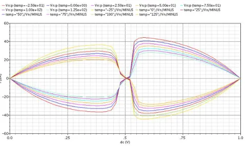
The read stability of an SRAM cell is conventionally measured by the cell read static noise margin (RSNM) [7]. To determine the read stability of an SRAM cell in a large array, BL current at the „0‟ storage node is measured while sweeping down the cell supply with the bit-lines pre-charged and WL driven by the nominal supply. The difference between the nominal supply and the cell supply causing BL current to drop gives the read margin of the SRAM cell. N curves -A new approach for read and write ability measure. N-curve, initially was first proposed by [10] for read stability curves also used as a measure of write ability. The unique feature of the N-curve is the use of the current information. In Fig.1, the cell initially holds„0‟ and both the two bitlines are clamped to Vdd. A dc sweep on node „1‟ (Qb) is performed to get the current curve through the dc source (Iin). The current curve crosses over zero at three points from left to right as shown in Fig.2.
4.
ANALYSIS OF READ & WRITE
STABILITY FOR PROPSED CELL USING
N CURVE METRICS
N curve for the proposed cell at Vdd =1V is shown. The N curve is being drawn is at various temperatures to analyze the effect of temperature on N curve. The N curve in Fig.2 is for the proposed cell at 45nm.
Fig. 2 N Curve for the proposed cell
[image:2.612.327.566.474.617.2]Vdd scaling limits the stability of the cell but it is not the only factor [12].But by increasing the transistor width we can have better stability at the expanse of area. To avoid a destructive read operation, the SVNM value should be as large as possible. SVNM indicates the maximum tolerable DC noise voltage at the input of the inverter of the cell before its content changes .For good write ability of the cell the value of WTV should be smaller. Smaller the value of WTV faster the cell is written. WTV will be lower than 0.5Vdd where pull up ratio is less than 1.[13].
[image:3.612.323.546.303.450.2]4.1
Read stability Matrix from N curve:
We have found the SVNM for the same cell with Vdd scaling and we can see that as Vdd scales the SVNM decreases. We have also seen that the effect of temperature as shown in the N curve in fig is negligible. The same analysis was done for SINM also. SINM is given by the peak value of Iin during read operation[13] .But in case of SINM we see that it does not depends only the Vdd but it varies with the temperature so temperature also holds a position for stability analysis in N curve. There is an exponential relation of SINM with the Vdd and it decreases with temperature. [image:3.612.55.292.349.512.2]Fig. 3 Read Stability: SVNM V/s Vdd
Fig. 4 Read stability: SINM V/s Vdd
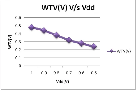
4.2 Write stability Matrix from N curve.
We have found the WTV for the same cell with Vdd scaling and we can see that as Vdd scales the WTV decreases. WTV is the voltage drop needed to flip the internal node “1” of the cell with both the bit lines clamped at Vdd .As we said that it should be less than 0.5Vdd and this is there in our cell. Analysis with temperature is also done but there is no significant change with temperature. The same analysis was done for WTI also. It is the amount of current needed to write the cell when both bit lines are clamped at supply voltage equal to Vdd.[10] But in case of WTI we see that it does not depends only the Vdd but it varies with the temperature so temperature also holds a position for stability analysis in N curve [10]. There is an exponential relation of WTI with the Vdd and it decreases with temperature. The ability to write a cell with both bit-lines clamped at results actually in a destructive read operation, therefore, the absolute value of WTI should be large enough to cope with the read stability requirement.Fig. 5 Write Stability: WTV with varying Vdd.
[image:3.612.53.290.423.682.2] [image:3.612.323.553.491.637.2]4.3 Effect of Vth Variation on N curve
matrix:
SINM & WTI depends on the variation of Vt .This is also observed when we simulated the cell at low Vt. We have replaced all the transistors with low Vt. In Table1 we have shown the variation of SINM&WTI with Vt variation at 25oC along with Vdd scaling.AT low Vdd the WTI and SINM has increased. Although the effect of Vt on WTV and SVNM is negligible.
Table I: Effect of varying Vt on Read Stability
At normal Vt At Low Vt
Vdd(v) SINM(A) WTI(A) SINM(A) WTI(A)
1 2.97E-05 3.79E-05 2.65E-05 3.23E-05
0.9 1.90E-05 2.69E-05 1.89E-05 2.47E-05 0.8 1.03E-05 1.66E-05 1.20E-05 1.72E-05 0.7 4.25E-06 7.87E-06 6.41E-06 1.03E-05 0.6 1.25E-06 2.39E-06 2.63E-06 4.63E-06
5. POWER ANALYSIS
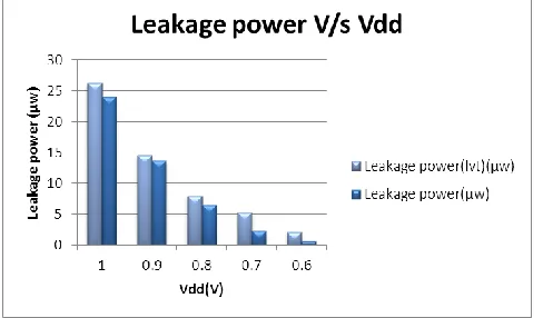
[image:4.612.48.297.205.370.2]We have calculated the read and write power from at 27oC .The Power were calculated at 1V & 0.5V. The Write „1‟ power measured was 32.32 µw and Write „0‟ power measured was 19.8 µw. Read „0‟ power measured was 23.89 µw at Vdd =1V. The Write „1‟ power measured was 545.9nw and Write „0‟ power measured was 450.5nw .Read „0‟ power measured was 110.8nw at Vdd=0.5V.Leakage power analysis has also been done at low Vt and at standard Vt. From Fig.7 it can be analyzed that low Vt the leakage power is increases.
Fig. 7 Leakage power V/s Vdd
6. CONCLUSION
In this proposed cell the read stability was being measured from SINM at 1V and at 50oC the SINM is 27µA and the SVNM is 520mv which is 28% higher than the earlier 9T SRAM cell.The SNM was 420mv at 1V 50oC. The cell has high write ability than the prior 9T SRAM cell[5]. The stability has been measure using N curve analysis .The analysis at low Vt has also been done as shown in table I. The read stability reduces when Vt is decreased but the write stability is unaffected. We have also calculated the read & write power which is useful for multimedia applications. And we can say that as we decrease the Vdd the cell read & write power reduces drastically. This cell is useful where high data stability is required.
7.
ACKNOWLEDGEMNET
The authors are very grateful to their respective organizations for encouraging them to complete this work.
8.
REFERENCES
[1].A. Bhavnagarwala, X. Tang, and J. Meindl, “ The impact of intrinsic device fluctuations on CMOS SRAM cell stability”. IEEE Journal of Solid-State Circuits (JSSC), 36:658–665, April 2001.
[2]. F. Yang, J. Hwang, and Y. Li., “Electrical characteristic fluctuations in sub-45 nm CMOS devices”. In Proc. of IEEE Custom Integrated Circuits Conference CICC, pages 691–694, September 2006.
[3]. F. Lai and C. Lee., “On-chip voltage down converter to improve SRAM read-write margin and static power for sub-nano CMOS technology”. IEEE Journal of Solid-State Circuits (JSSC), 42:2061–2070, September 2007.
[4]. Sinangil M., Naveen Verma, A.P.Chandrakasan, “ A Reconfigurable 8T Ultra –Dynamic Voltage Scalable( U-DVS ) SRAM in 65nm CMOS” , Solid-State Circuits,
IEEE Journal ,vol. 44 , no. 11,Nov.2009, pp.3163-3173. [5]. Zhiyu Liu and Volkan Kursun, “Characterization of a Novel
Nine-Transistor SRAM cell”, IEEE Transaction of Very large Scale Integration Systems, vol. 16, NO. 4, April 2008,pp.488-492
[6]. Sheng Lin, Yong-Bin Kim , Fabrizio Lombardi., “Design and analysis of a 32 nm PVT tolerant CMOS SRAM cell for low leakage and high stability” Integration the VLSI Journal, vol. 43 ,January 2010, pp. 176-187.
[7]. Zheng Guo, Andrew Carlson, Liang-Teck Pang, Kenneth Duong, Tsu-Jae King Liu, Borivoje Nikolic, “Large-Scale Read/Write Margin Measurement in 45nm CMOS SRAM Arrays”,IEEE Symposium on VLSI Circuits Digest of Technical Papers 2008,pp-42-43.
[image:4.612.53.297.515.658.2][9]. E. Seevinck et al., “Static-noise margin analysis of MOS SRAM cells,”IEEE J. Solid-State Circuits, vol. SC-22, no. 5, pp. 748–754, Oct. 1987.
[10]. Evelyn Grossar, Michele Stucchi, Karen Maex,” Read Stability and Write-Ability Analysis of SRAM Cells for Nanometer Technologies”, Solid-State Circuits, IEEE Journal ,vol. 41 , no. 11, Nov.2006, pp.2577-2588. [11]. Shilpi Birla, Manisha Pattanaik, R.K.Singh “Static Noise
Margin Analysis of Various SRAM Topologies”, IACSIT International Journal of Engineering and Technology, Vol.3, No.3, June 2011,pp-304-309
[12]. Shilpi Birla, Neeraj Kr. Shukla, Manisha Pattanaik, R.K.Singh, “Device and Circuit Design Challenges for Low Leakage SRAM for Ultra Low Power Applications”, Canadian Journal on Electrical & Electronics Engineering Vol. 1, No. 7, December 2010.
[13] Benton H. Calhoun Anantha P. Chandrakasan “Static Noise Margin Variation for Sub-threshold SRAM in 65 nm CMOS”, Solid-State Circuits, IEEE Journal vol. 41, Jan.2006, Issue 7, pp.1673-1679.
.