1
Advanced post-acceleration methodology for pseudospark-sourced electron
beam
J. Zhao
1,2,3,a), H. Yin
3, L. Zhang
3, G. Shu
3, W. He
3, Q. Zhang
1,2, A. D. R. Phelps
3and A. W. Cross
31State Key Laboratory of Electrical Insulation and Power Equipment, Xi’an, 710049, China
2High Voltage Division, School of Electrical Engineering, Xi’an Jiaotong University, Xi’an, 710049, China 3Department of Physics, SUPA, University of Strathclyde, Glasgow, G4 0NG, Scotland, United Kingdom
During its conductive phase, a pseudospark discharge is able to generate a low energy electron beam with a higher combined current density and brightness compared with electron beams formed from any other known type of electron source. In this paper, a configuration is proposed to post-accelerate an electron beam extracted from a single-gap pseudospark discharge cavity in order to achieve high quality high energy intense electron beams. The major advancement is that the triggering of the pseudospark discharge, the pseudospark discharge itself and the post-accelerating of the electron beam are all driven by a single high voltage pulse. An electron beam with beam current of ~20 A, beam voltage of 40 kV and duration of ~180 ns has been generated using this structure. The beam energy can be adjusted through adjusting the amplitude of the voltage pulse and the operating voltage of the whole structure which can be varied from 24 to 50 kV with an efficient triggering method under fixed gas pressure below ~10 Pa.
I. INTRODUCTION
Pseudospark-sourced electron beam has been recognized as an electron beam source with higher combined brightness (up to 1012A/m2rad2) and current density (can be higher than 108A/m2) than other electron
beam source1-4. The self-focusing feature of the
pseudospark-sourced electron beam also offers the additional benefit of not requiring any external guiding magnetic field, which can greatly simplify the system. A pseudospark-sourced electron beam has been applied in many fields such as material process, free electron laser, x-ray source and microwave devices5-8. Recently, the
operating frequency of microwave devices is extending to the THz region in which the size of the beam-wave interaction region is down to the submillimeter range and much higher driving electron beam current density is required. This makes the pseudospark-sourced electron beam a promising candidate for driving THz radiation sources4,9,10.
The pseudospark discharge of single-gap or multi-gap structure can be considered roughly to evolve in three main stages: 1) Townsend discharge; 2) hollow cathode discharge and 3) the final conductive discharge. In the Townsend discharge stage, a plasma or virtual anode starts to form in the discharge gap and the discharge current is relatively small. Only during the hollow cathode discharge stage, an intense electron beam with high beam energy can be extracted from the discharge gap. In the conductive stage, the electron beam current is much higher than in
stage 2 but the beam energy is limited because the voltage across the discharge gap has already collapsed. Due to the transient nature of the pseudospark discharge, the duration of the high energy electron beam is limited to a narrow range of about 10 ~ 30 ns according to most experimental results on various pseudospark discharge structures2,11-14.
The discharge voltage of the pseudospark discharge is sensitive to gas pressure and varies greatly in a narrow gas pressure range while the discharge voltage also varies due to the statistical property of the discharge process even under a fixed gas pressure15-17, which may cause some
stability problems of the devices driven by pseudospark-sourced electron beams.
The duration of the conductive stage is much longer but the low energy electron beam cannot be used to drive any energy-sensitive devices. It would be a great advantage for devices driven by pseudospark-sourced electron beams if the low energy electron beam in the conductive stage can be further accelerated, that is the so called post-acceleration, after its extraction from the discharge gap to a high energy with a much longer duration. In this paper, a simple configuration including only one high voltage pulse generator and a single-gap pseudospark discharge cavity with a post-acceleration gap has been constructed to achieve the triggering, driving of the pseudospark discharge and the post accelerating of the electron beam. A stable trigger method is designed to ensure the operating pulsed voltage is much lower than the self-breakdown voltage of the pseudospark discharge gap and is insensitive to the gas pressure too, thus the proper structure and operation conditions of the pseudospark a)
2
discharge and the post-acceleration structure of the electron beam are determined for this purpose.
II. CONFIGURATION OF THE POST-ACCELERATION OF THE PSEUDOSPARK-
The system includes a high voltage pulse generator and a single gap pseudospark discharge cavity with post-acceleration gap, two high voltage probes, Vprob1 and Vprob2,
and a Faraday cup used to measure the voltage pulses and the electron beam current respectively, as presented in figure 1.
There is a small through hole of diameter of 2 mm at the end of the hollow cathode cavity while the rodlike head of the trigger electrode of diameter of 1.6 mm inserts into this hole and forms a very small discharge gap of 0.2 mm, which serves as a trigger gap of the pseudospark discharge. This trigger gap will breakdown first and all of the
discharge current will flow through the discharge channel and then provides seed electrons to start the pseudospark discharge.
The diameter and depth of the hollow cathode cavity are 26 mm and 12 mm respectively. The apertures of the cathode, the anode and the grounded flange are all of diameters of 3 mm and all edges of the apertures are rounded off with radius of 1 mm to avoid much higher electrical field near the sharp edges and prevent undesired discharge process. The pseudospark discharge gap separation of 16 mm18 is used to get relatively high beam
current and the post-acceleration gap separation is 6 mm. A groove-like fold structure on the inner surface of the cathode-anode spacer to prolong the creepage distance and prevent surface flashover across the pseudospark discharge gap.
This two-gap configuration is different from multi-gap pseudospark discharge configuration. In the multi-gap pseudospark discharge configuration, each gap breaks down successively from the cathode to the anode during the discharge and a high energy electron beam is generated during the breakdown process, while in this two-gap pseudospark discharge and post-acceleration configuration, the discharge gap serves as a low energy electron beam source after its breakdown and the second gap serves to
a. Post acceleration structure of the pseudospark sourced
electron beam source
[image:2.612.320.559.73.392.2]b. Electrode diagram of the post-acceleration structure
FIG. 1. Post-acceleration configuration of the pseudospark
sourced electron beam. trigger electrode ○1, trigger discharge gap
○2, pseudospark cathode ○3, hollow cathode cavity ○4, cathode
aperture ○5, pseudospark discharge gap ○6, pseudospark anode
with output aperture ○7, post-acceleration gap ○8, grounded
flange with output aperture○9, Faraday cup (FC) 10○. Structures
with white and brass colors are insulating and metallic parts, respectively.
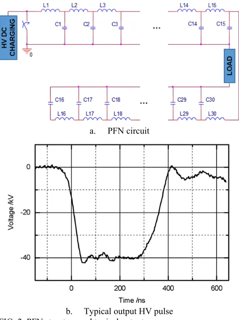
a. PFN circuit
b. Typical output HV pulse
[image:2.612.51.286.100.456.2]3
accelerate the electron beam to subsequent certain energy level.
A Faraday cup is placed 18 mm downstream after the grounded flange to detect the beam current. A 10 Ω
sampling resister is connected directly to the Faraday cup to convert the beam current to voltage signal Vfc which
transmits through a 3 m long cable and a 10:1 voltage divider connected to the input port of an oscilloscope (Tektronix TDS 640). Pulsed voltages on the cathode and the anode of the pseudospark discharge gap are detected by two high voltage probes (1000:1 Tektronix P6015A, presented in figure 1 as Vprob1 and Vprob2) and recorded on
the same oscilloscope. A 200 Ω high voltage resister connects the anode and the grounded flange, the effect of this resister will be discussed in the next section.
The high voltage pulse generator is a PFN (pulse forming network) Blumlein generator consisting of two 15-stage PFNs. A pulse forming network (PFN) is an electric circuit that accumulates electrical energy over a comparatively long time then releases the stored energy in the form of a relatively square pulse of comparatively brief duration, in which, energy storage components are charged by means of a high voltage power source then rapidly discharged into a load through a high voltage switch. The energy storage capacitor c0 is 0.76 nF and inductance l0 is about
186 nH for each stage of the PFN. The pulse width is ~356 ns and the characteristicimpedance of the Blumlein PFN is 2 ⁄ 31 Ω. Circuit structure and typical pulse output are presented in figure 2.
III. EXPERIMENTS
When the high voltage pulse from the PFN generator is applied between the trigger electrode and the grounded flange, the voltage will redistribute on the stray capacitance cx ≈ 2.5 pF of the trigger discharge gap, the
stray capacitance cm ≈ 14.2 pF of the pseudospark
discharge gap and the resister RB. Because cx is much
smaller than cm, most of the voltage will drop on the
trigger gap before the breakdown of the pseudospark discharge gap. Although within the operating pressure
range of the pseudospark discharge the pd of the trigger gap is much lower than pd of the pseudospark discharge gap and the hold-off voltage of the trigger gap should be much higher than that of the pseudospark discharge gap, but the electrical field strength is extremely high due to the very small gap separation and the field emission of the electrons dominates the discharge process in the trigger gap. So the breakdown voltage of the trigger gap is actually much lower than that of the pseudospark discharge gap and the first breakdown definitely takes place in the trigger gap when a sufficient high voltage is applied over the whole structure. Because the trigger gap is serially connected in the structure, all of the discharge current will pass through the discharge channel during the discharge and produces sufficient seed electrons to start the pseudospark discharge.
After the trigger gap breaks down, in the first 2 stages of the pseudospark discharge, the discharge current is very limited and the voltage on resistor RB is much smaller than
the voltage of the driving pulse, so most of the voltage drops on the pseudospark discharge gap. In the conductive stage of the pseudospark discharge, because the voltage across the pseudospark gap has collapsed and the voltage across the gap keeps at a low level and then the total voltage is nearly applied on the resistor RB and the
accelerated gap before its breakdown.
The resistor RB is a key component in the device to
ensure the pseudospark gap discharging prior to any discharge in the acceleration gap and the voltage drops mainly on the trigger gap and the pseudospark gap in the first two stages of the pseudospark discharge. Meanwhile it limits the voltage on the acceleration gap to a low level during this period to limit the discharge and initial plasma in the acceleration gap before the conductive stage of the pseudospark discharge. The resistance of RB needs to be
much higher than the characteristic impedance Z0 to
maintain the PFN generator output with voltage of 2U0
4
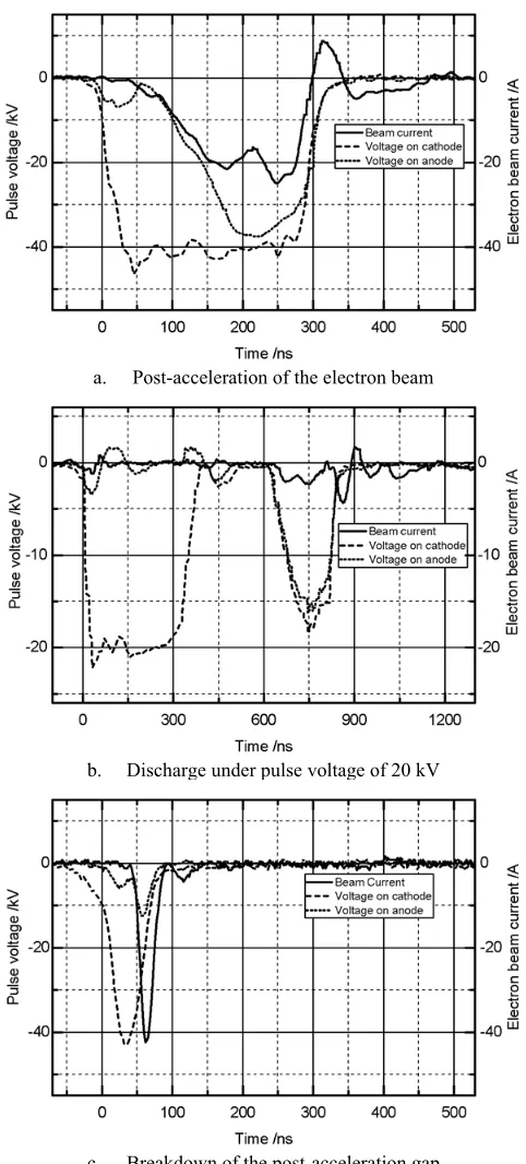
According to figure 3, during the front edge of the voltage pulse on the structure, most of the voltage are applied over the trigger gap and the pseudospark gap, while the voltage over the resister RB is only ~ 6 kV with
duration of ~ 50 ns, which corresponds to the charging process of the stray capacitance cx and cm. After the 50 ns,
the electron beam current and the post-acceleration voltage start to rise simultaneously. The electron beam pulse width is about 180 ns and the voltage at both the cathode and the anode keeps high during this period. The voltage at the anode is 2~3 kV lower than the voltage at the cathode, which corresponds to the voltage drop on the pseudospark discharge gap.
The biggest challenge is to ensure the discharge of the pseudospark gap and to avoid the breakdown of the acceleration gap at the same time under the similar conditions. The post-acceleration voltage rises as the electron beam injects into the post-acceleration gap simultaneously. Because the electron beam current is much higher than that in the initial stage of the pseudospark discharge gap, so the acceleration gap is much easier to breakdown than the pseudospark discharge gap under similar conditions. As presented in figure 3c, when the acceleration voltage rises to a certain level, the post-acceleration gap breakdowns immediately. The breakdown process is sensitive to the gas pressure and also influenced by the structure. Breakdown between the electrodes of the post-acceleration gap or flashover of the inner surface of the insulating spacer occur immediately after the electron beam injection into the post-acceleration gap when the gas pressure is over 15 Pa in this configuration.
Because the pd of the post-acceleration gap is on the left hand branch of the Paschen curve, in order to improve the hold-off voltage of the gap, the gap separation needs to be as small as possible. But the reduced gap separation enhances the electrical field strength furthermore and limits the creepage distance of the inner surface of the insulating spacer, which increases the possibility of the surface flashover. In addition, much higher electrical field strength will cause undesired electron emission and discharge process. So in this post-acceleration configuration, a gap separation of 6 mm is chosen as the compromise requirements on the pd of the acceleration gap and creepage distance of the spacer under the gas pressure in the regime of the pseudospark discharge. Separations of 0.5 mm between the electrodes and the spacer formed by 0.5 mm steps on both sides of the spacer at the triple junction of the electrode-spacer-gas was chosen to reduce the electrical field strength at the point.
Because the proper gas pressure for the acceleration gap is only under 10 Pa, this restricted range of the gas pressure may significantly limit the operating voltage range of the pseudospark structure.The discharge in the
trigger gap can provide enough electrons to start the pseudospark discharge process. Although the self-breakdown voltage of the pseudospark structure without triggering is much higher than the operating voltage of the structure, pseudospark discharge process can be obtained for voltage pulse with amplitude of about 24 to 50 kV
a. Post-acceleration of the electron beam
b. Discharge under pulse voltage of 20 kV
[image:4.612.320.561.74.607.2]c. Breakdown of the post-acceleration gap
5
under the same gas pressure below 10 Pa due to the efficient triggering of the trigger gap.
The electron beam currents increase from several to more than 30 amperes with increasing pulse voltage in the operating range. Meanwhile, with increasing pulse voltage up to ~40 kV the beam durations increase from tens of nanoseconds to less than 200 nanoseconds and then significantly reduce when pulse voltage approaches 50 kV. When the applied pulse voltage goes down below 24 kV, the trigger gap can still breakdown due to the high electrical field but the discharge in pseudospark gap may be absent frequently due to the relative low voltage. With the absence of the pseudospark discharge, multi-pulses with decreasing amplitude, which is generated by multiple reflections of the voltage pulse between pseudospark gap and pulse generator, then applied on the pseudospark gap and the pseudospark discharge may occur at the second or even the third or fourth pulse as shown in figure 3b. When the applied voltage goes up above 50 kV, the acceleration gap may breakdown quickly after the electron beam with higher current and voltage injected into the gap, similar to the situation in figure 3c.
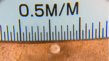
To estimate the electron beam density, a copper foil with thickness of 50 μm is placed 6 mm downstream after the grounded flange to capture the beam spot produced by bombarding of the electron beam ~ 300 times, as presented in figure 4. The diameter of the beam spot is ~1.5 mm, so the electron beam density can be estimated to be ~1.1 kA/cm2 according to the electron beam current and its spot
diameter.
IV. CONCLUSION
In this paper, a simple pseudospark-sourced electron beam source including a PFN Blumlein high voltage pulse generator and a single gap pseudospark discharge cavity with post-acceleration structure has been built. The triggering, driving of the pseudospark discharge and the post accelerating of the electron beam can be achieved by only one PFN high voltage pulse. The pseudospark discharge in this structure can be performed under a range
of pulsed voltage at the same gas pressure independent of the pd of the structure. With the efficient triggering method, an electron beam of ~20 A current and ~180 ns duration has been obtained when a 40 kV voltage pulse is applied.
1 Y. Huang, M. C. Wang, and Z. J. Wang, Chinese Science Bulletin 43,
260 (1998).
2 W. Benker, J. Christiansen, K. Frank, H. Gundel, W. Hartmann, T.
Redel, and M. Stetter, Plasma Science, IEEE Transactions on 17, 754
(1989).
3 J. Christiansen and C. Schultheiss, Zeitschrift für Physik A Atoms and
Nuclei 290, 35 (1979).
4 W. He, L. Zhang, D. Bowes, H. Yin, K. Ronald, A. D. R. Phelps, and
A. W. Cross, Applied Physics Letters 107 (2015).
5 S. V. Lebedev, M. Machida, S. A. Moshkalyov, and D. O. Campos,
Ieee Transactions on Plasma Science 25, 754 (1997).
6 J. B. Zhu, M. C. Wang, Z. J. Wang, and J. K. Lee, Optical Engineering
35, 498 (1996).
7 C. S. Wong, H. J. Woo, and S. L. Yap, Laser and Particle Beams 25,
497 (2007).
8 A. W. Cross, H. B. Yin, D. Bowes, W. L. He, K. Ronald, and A. D. R.
Phelps, in New Developments in Nonlinear Plasma Physics; Vol. 1188
(2009), p. 380.
9 T. Schuhmann, J. Protz, D. Fields, H. Yin, A. Cross, W. He, D. Bowes,
K. Ronald, and A. Phelps, in Millimetre Wave and Terahertz Sensors
and Technology Iii; Vol. 7837 (2010).
10 Y. Yin, W. L. He, L. Zhang, H. B. Yin, C. W. Robertson, and A. W.
Cross, Ieee Transactions on Electron Devices 63, 512 (2016).
11 E. Boggasch, T. A. Fine, and M. J. Rhee, Proceedings of the 1989 Ieee
Particle Accelerator Conference, Vols 1-3, 316 (1989).
12 E. Dewald, K. Frank, D. H. H. Hoffmann, M. Ganciu, N. B. Mandache,
M. Nistor, A. M. Pointu, and I. I. Popescu, Nuclear Instruments & Methods in Physics Research Section a-Accelerators Spectrometers
Detectors and Associated Equipment 415, 614 (1998).
13 C. Q. Jiang, A. Kuthi, M. A. Gundersen, and W. Hartmann, Applied
Physics Letters 87 (2005).
14 M. Nistor and N. Mandache, J. Optoelectron. Adv. Mater 7, 1619
(2005).
15 H. Yin, W. He, A. W. Cross, A. D. R. Phelps, and K. Ronald, Journal
of Applied Physics 90, 3212 (2001).
16 J. Zhang, J. Zhao, and Q. Zhang, IEEE Transactions on Plasma Science
42, 2037 (2014).
17 J. Zhang, J. Zhao, and Q. Zhang, IEEE Transactions on Plasma Science
42, 3886 (2014).
18 J. Zhao, H. Yin, L. Zhang, G. Shu, W. He, J. Zhang, Q. Zhang, A. D. R.
[image:5.612.55.281.585.711.2]Phelps, and A. W. Cross, Physics of Plasmas 23, 073116 (2016).