DESIGN OF MULTI-BAND BANDPASS FILTER FOR NEXT GENERATION WIRELESS SYSTEM
LEE KAH WENG
This report submitted in partial fulfillment of the requirements for the award of Bachelor of Electronic Engineering (Telecommunications Electronics) With
Honours
Faculty of Electronics and Computer Engineering Universiti Teknikal Malaysia Melaka
UNIVERSITI TEKNIKAL MALAYSIA MELAKA
UNIVERSTI TEKNlKAL MALAYSIA MELAKA
FAKULTI KEJURUTERAAN ELEKTRONIK DAN KEJURUTERAAN KOMPUTER
BORANGPENGESAHANSTATUSLAPORAN
PROJEK SARJANA MUDA II
Tajuk Projek
DESIGN OF MULTI-BAND BANDPASS FILTER FOR NEXT
GENERATION WIRELESS SYSTEM
Sesi
Pengajian 4
Saya LEE KAH WENG
I 5
(HURUF BESAR)
mengaku membenarkan Laporan Projek Saijana Muda ini disimpan di Perpustakaan dengan syarat-syarat kegunaan seperti berikut:
I. Laporan adalah hakmilik Universiti Teknikal Malaysia Melaka.
2. Perpustakaan dibenarkan membuat salinan untuk tujuan pengajian sahaja.
3. Perpustakaan dibenarkan membuat salinan laporan ini sebagai bahan pertukaran antara institusi pengajian tinggi.
4. Sila tandakan ( -V ) :
D
SULIT ..D
TERHADH0
TIDAK TERHAD*(Mengandungi maklumat yang berdarjah keselamatan atau kepentingan Malaysia seperti yang termaktub di dalam AKT A RAHSlARASML 1972)
**(Mengandungi maklumat terhad yang telah ditentukan oleh organisasi/badan di mana penyelidikan dijalankan)
Disahkan oleh:
( f A N D A e PENULIS)
. II
I
b / .2.01'?
Tankh: ... .
DR. ZAHRILADHA BIN ZAKARIA
Profesor Madyo
Fikul1l Kejunrtm;n Elektronlk oan Ke)uruteraan lCo;npi.~}f.
Unlversltl Teknlkal Malaysia ivlelaka {U1eM
Hang Tuah Jaya
76100 Durian Tungr,al, M~I~~~
DECLARATION
I declared that this thesis entitled "DESIGN Of MULTI-BAND BANDPASS
f!LTER fOR NEXT GENERATION WIRELESS SYSTEM" is the result of my
own research except as cited in the reference.
Signature
Author
Date
: LEE KAH WENG
II
(fo(
'U)I~lV
APPROVAL
l hereby declare that I have read this thesis and in my opinion this thesis is su±licient
in term of the scope and quality for the award of Bachelor of Electronic Engineering
(Telecommunication Electronics) With Honors.
Signature
Supervisor's Name
Date
-~~~
: PM. DR. ZAI-I:ill:!A BIN ZAK.ARIA
v
DEDICATION
Special dedication to my beloved parents, Lee Wing Fook & Kong Lai Peng
My supporting siblings:
Lee Poh Yoke Lee Kah Meng
To my supervisor
PM Dr Zahriladha Bin Zakaria
My friends and my fellow lecturers
vi
ACKNOWLEDGMENT
vii
ABSTRACT
viii
ABSTRAK
ix
TABLE OF CONTENTS
CHAPTER CONTENTS PAGES
TITLE i
DECLARATION iii
APPROVAL iv
DEDICATION v
ACKNOWLEDGMENT vi
ABSTRACT vii
ABSTRAK viii
TABLE OF CONTENTS ix
LIST OF FIGURES xii
LIST OF TABLES xv
I. INTRODUCTION
1.1 Introduction 1
1.2 Problem statement 2
1.3 Objective 2
1.4 Scope of project 3
1.5 Chapter review 3
II. LITERATURE REVIEW
2.1 Band pass filter 5
2.2 Planar microstrip band pass filter 6
2.3 Multi-band band pass filter 7
x
2.5 Related research 8
III. METHODOLOGY
3.1 Methodology 15
3.2 Designing multi-band band pass filter 17 3.2.1 Filter specification and parameter 18 3.2.2 Design technique, equation and calculation 19
3.2.3 Ideal transmission line 23
3.2.4 Microstrip line 24
3.2.5 Layout structure 26
3.3 Defected microstrip structure (DMS) 26
3.3.1 Parametric study 26
3.4 Bandpass filter integrated with DMS 27
3.5 Fabrication and measurement 28
IV. RESULT & DISCUSSION
4.1 Multi-band bandpass filter ideal transmission line
structure 30
4.2 Microstrip line structure 33
4.2.1 Microstrip line structure with T-junction 34 4.2.2 Symmetric width and length of bandpass
filter 39
4.3 Parametric study on defected microstrip structure
(DMS) 41
4.4 Bandpass filter integrated with DMS 46 4.5 Physical structure and comparison result of
xi
V. CONCLUSION
5.1 Conclusion 52
5.2 Future works 53
REFERENCES 54
APPENDICES
Appendix A Gantt chart 57
Appendix B Poster INOTEK 2015 58
Appendix C INOTEK 2015 certificate 59
xii
LIST OF FIGURES
FIGURE TITLE PAGES
2.1 Frequency response of band pass filter 6
2.2 Example of planar microstrip band pass filter 6 2.3 Notched responses introduced to remove unwanted
frequency range 7
2.4 DMS structure on the microstrip 8
3.1 Flow chart of designing multi-band band pass filter 16 3.2 Process to design multi-band band pass filter 17 3.3 Topology of quarter-wavelength short-circuited stubs
filter 19
3.4 The table of element values of Cheyshev low pass prototype
filter 20
3.5 Schematic of ideal transmission line of band pass filter. 23
3.6 Setting of “LineCalc” 24
3.7 Schematic of microstrip line structure based on the
value of table 3.4 25
3.8 Layout structure of bandpass filter 26
3.9 Different shape of DMS designed (hashtag, U, C) 26
3.10 Bandpass filter without defaced 27
3.11 Bandpass filter has been defaced 28
3.12 Layout in CorelDraw software 28
3.13 DUT (device under test) by using VNA 29
4.1 Ideal transmission line of band pass filter 30 4.2 Simulation result of ideal transmission line 31
xiii
4.4 Schematic of ideal transmission line after tuning 32 4.5 Simulation result of transmission line after tuning 32 4.6 Schematic of microstrip line structure. (without MTEE) 33 4.7 Simulation result of microstrip line structure. (without
MTEE) 33
4.8 Layout of bandpass filter structure 34
4.9 Setting of via ground 34
4.10 Schematic of microstrip line structure. (with MTEE) 35 4.11 Simulation result of microstrip line structure. (with
MTEE) 35
4.12 Microstrip line structure (with MTEE) of bandpass filter
after tuning 37
4.13 Simulation of microstrip line structure (with MTEE) of
bandpass filter after tuning 37
4.14 Layout structure of bandpass filter after tuning 38 4.15 Simulation of layout structure (with MTEE) of bandpass
filter after tuning 38
4.16 Schematic of bandpass filter 39
4.17 Layout structure of symmetric bandpass filter 40 4.18 Simulation result from the layout structure 41
4.19 Dimension of DMS 42
4.20 EM simulation result by adjusting ‘a’ 42
4.21 EM simulation result by adjusting ‘d’ 43
4.22 EM simulation result by adjusting ‘b’ 44
4.23 EM simulation result by adjusting ‘c’ 44
4.24 EM simulation result by adjusting ‘e’ 45
4.25 Layout structure of bandpass filter integrated with
first U-shape DMS 46
4.26 Simulation result of bandpass filter integrated with
first U-shape DMS 46
4.27 Layout structure of bandpass filter integrated with second
xiv
4.28 Simulation result of bandpass filter integrated with second
U-shape DMS 47
4.29 Layout structure of multi-band bandpass filter integrated
with two U-shape DMS 48
4.30 Simulation result of multi-band bandpass filter integrated
with two U-shape DMS 48
4.31 Current flow visualization of multi-band bandpass filter
integrated with DMS 48
4.32 Current flow visualization of multi-band bandpass filter
integrated with DMS 49
4.33 Physical structure of multi-band bandpass filter 50 4.34 Measurement result of multi-band filter by using
Vector Network Analyzer (VNA) 50
4.35 Comparison between simulation result and measurement
xv
LIST OF TABLES
TABLE TITLE PAGES
2.1 The information of related research papers 8 3.1 Specification and parameter of band pass filter 18
3.2 Specification of Roger 4350B substrate 18
3.3 Value of admittances and impedances after
calculating the equation given 22
3.4 Value of width and length used to construct
microstrip line schematic 25
3.5 Specification of defected microstrip structure 27 4.1 The values of microstrip linestructure (with
MTEE) before tuning and after tuning 36 4.2 The symmetric width and length of short
1
CHAPTER I
INTRODUCTION
1.1 Introduction
Wireless communication has been rapidly developing in recent years. The evolution has started with Global System for Mobile Communications (GSM) and has proceeded to Wireless Local Area Network (WLAN), Worldwide Interoperability for Microwave Access (WiMAX), Code Division Multiple Access (CDMA), and the latest, Long Term Evolution (LTE) and Fifth Generation (5G). Microwave filters are required in microwave systems to separate wanted and unwanted signals. Recently, multi-band microwave filters developed by various researchers to satisfy the current demands of wireless communication systems. Before, single-band filters can only operate in single-frequency bands are used. After researching and demanding, dual-band and tri-band or multi-band microwave which can be supported in a single device are needed. A single device has the ability to work in multiple frequencies and support various wireless communications such as GSM, WLAN, WiMAX and LTE is one of the requirements for global devices [1].
2
independent of the microstrip length which can be very useful in the design of microstrip filters, among other different applications. In this proposed project, a new design of triple-band band pass filter integrated with DMS [2].
1.2 Problem statement
Development in wireless communication has created more potential in IEEE 802 family local area networks and metropolitan area networks. They able to support high speed wireless broadband applications with rather long reach, mobility, and roaming. The most latest wireless communication network LTE or Long Term Evolution UMTS networks have made strong inroads into the commercial arena worldwide. So, a single microwave filter which can support multiple wireless applications is strongly demanded. The challenges to circuit designers designing a multi-band band pass filter are to achieve compact size and low insertion loss simultaneously. The previous works are usually too many components inside and cause large circuit size. Besides of the ability to support various wireless communication applications, also need to satisfy the specifications of band pass filter which are size reduction, high stability, high selectivity simultaneously [3].
1.3 Objective
3
1.4 Scope of project
The design of this proposed project is multi-band band pass filter. The topology of the band pass filter is quarter wavelength short-circuited stubs with Defected Microstrip Structure (DMS). The pass band bandwidth of the filter is 2.3-2.7GHz, 3.1-4.8GHz and 5.15-5.85GHz at -3dB. The pass band return loss is better than -20dB whereas the pass band insertion loss is between 0dB till -1dB. Besides, the stop band insertion loss is better than 40dB. Before fabrication, design and simulate the filter and DMS in Advanced Designed System (ADS) software. The material used to fabricate this filter is Roger 4350B with dielectric constant of 3.48 and loss tangent of 0.0019. This filter is done with equation of short circuited stubs and the introduced notched responses. The DMS technology is carried out using a parametric study to provide the shape and better performance in term of selectivity.
1.5 Chapter review
Chapter I mainly describes the general overview of this project. Chapter 1 explains the introduction, problem statement, objective and scope of this project. Besides, this chapter also reviews all chapters of this project.
Chapter II mainly describes findings on a literature review of the project. It covers related research from band pass filter, dual-band band pass filter, tri-band band pass filter, multi-band band pass filter and DMS. The chapter starts with the basic theory and fundamental of the filter. The basic understanding of the parameters and the basics of microwave filter must be clearly made before continuing on understanding the project. The most important part of this chapter is emphasizing literature on different technique designing band-pass filter.
4
Chapter IV will illustrate, explain, discuss and present the simulation result and measurement result of multi-band bandpass filter. For the implementation of this project, design start from ideal transmission line structure, then microstrip line structure, next momentum layout structure and last physical structure of multi-band bandpass filter.
5
CHAPTER II
LITERATURE REVIEW
In this chapter, it describes findings on a literature review of the project. Overall, it covers related research from band pass filter, dual-band band pass filter, tri-band band pass filter, multi-band band pass filter and DMS. The chapter starts with the basic theory and fundamental of the filter. The basic understanding of the parameters and the basics of microwave filter must be clearly made before continuing on understanding the project. The most important part of this chapter is emphasizing literature on different technique designing band-pass filter.
2.1 Band pass filter
6
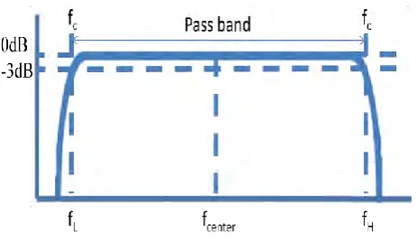
Figure 2.1: Frequency response of band pass filter.
2.2 Planar microstrip band pass filter
Microstrip line is one of the most popular types of planar transmission lines primarily because it can be fabricated by photolithography processes and is easily miniaturized and integrated with both passive and active microwave devices. Figure 2.2 shows the example of planar microstrip band pass filter. The planar transmission line is a transmission line with conducting metal strips that lie entirely in parallel planes. The most common structure has one or more parallel metal strips placed on a dielectric substrate over a conducting ground plane. All the active devices and all the interconnecting lines, impedance-matching elements, capacitors, inductors and resistors are fabricated on the planes [5].
[image:21.595.162.484.565.679.2]7
2.3 Multi-band band pass filter
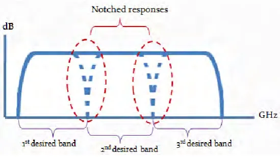
[image:22.595.183.458.236.390.2]Multi-band band pass filter is the filter which has three desired frequency bands by introducing notched responses as illustrated in Figure 2.3. The notched responses will remove the unwanted frequency bands and introduce the desired frequency bands for multiple wireless communication applications.
Figure 2.3: Notched responses introduced to remove unwanted frequency range.
2.4 Notched responses
8
Figure 2.4: DMS structure on the microstrip.
2.5 Related research
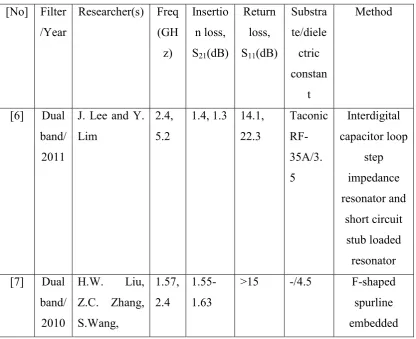
In order to implement this project, findings and researches about the bandpass filter have been done and tabulated as shown in Table 2.1.
Table 2.1: The information on related research papers.
[No] Filter /Year
Researcher(s) Freq (GH
z)
Insertio n loss, S21(dB)
Return loss, S11(dB)
Substra te/diele ctric constan t Method
[6] Dual band/ 2011
J. Lee and Y. Lim
2.4, 5.2
1.4, 1.3 14.1, 22.3 Taconic RF-35A/3. 5 Interdigital capacitor loop step impedance resonator and short circuit stub loaded resonator [7] Dual
band/ 2010
H.W. Liu, Z.C. Zhang, S.Wang,
1.57, 2.4
1.55-1.63
[image:23.595.112.529.418.757.2]9
L.Zhu,X.H.G uan,J.S.Lim and D. Ahn
into uniform impedance
resonator [8] Dual
band/ 2012
M.T. Doan, W.Q. Che and W.J. Feng 2.4, 5.2 Minim um 0.85
>20 -/4.4 Short-stub loaded half wavelength resonator [9] Tri
band/ 2012
A.M. Elelimy, A.M. El-Tager, A.G. Sobih and M.H. Abdel-Azeem 0.9, 2.45, 3.5 0.85, 1.12, 1.16 10.8, 18.14, 16.25 Roger RT/Dur oid 6010 Teflon/ 10.5 Cross coupled resonators to produce tri-section step impedance resonator
[10] Tripl e band/ 2011 C.Y.Lin, W.T.Li, C.P.Liang and S.J.Chung 2.4, 3.5, 5.2
- >10 - Cascade
grounded active inductor
circuit topology [11]
Tri-band/ 2011 Z.B.Wang, F.Nasri, C.W.Park 6.42, 10.7, 14.9 8 15.7, 31.7, 30.1
- Duroid
5880/2. 2
Interdigital hairpin finger
structure
[12] Tripl e band/ 2014 J.P.Wang, J.D.Zhao, J.L. Li 5.2, 5.8, 8.0
>15 <15 Duroid 5880/3. 38 Parallel U-shaped defected microstrip structure [13] Tripl
e-band/
2012
M.M.Prabhak
ar and