Nanolithography: Status and Challenges
Rashed Md. Murad Hasan, Xichun Luo
Centre for Precision Manufacturing, Department of Design, Manufacture & Engineering Management University of Strathclyde, Glasgow, United Kingdom
Abstract—With the help of immersion lithography and multiple patterning, photolithography has been the key technology over the last decade in manufacturing of ICs, microchips and MEMS devices. Continuous rapid shrinking of feature size made the authorities to seek alternative patterning methods that can go beyond classic photographic limits. Some promising techniques have been proposed as next generation lithography and further technological progress are required to make them significant and reliable to meet the current demand. EUVL is considered as the main candidate for sub-10 nm manufacturing because of its process simplicity and reduced operating cost. Remarkable progress in EUVL has been made and the tools will be available for commercial operation soon. EBL, FIB and X-ray lithography are used for patterning in R&D, mask/mold fabrication and low volume chip design. DSA have already been realized in lab and further effort will be needed to make it as NGL solution. NIL has emerged attractively due to its simple process-steps, high-throughput, high-resolution and low cost and become one of the commercial platforms for nanofabrication.
Keywords-Nanolithography; NGL; throughput; resolution; patterning;
I. INTRODUCTION
Photolithography has been the dominant method of patterning nanoscale features for the microelectronics industries since the commencement of the ICs. Resolution Enhancement Technologies (RET) and Immersion method enable the photolithography with patterning beyond its intrinsic resolution limit. RET improves the quality of an image. It generally includes phase shift mask, optical proximity correction (OPC), modified or off-axis illumination (OAI), and multiple patterning. Although, they have extended the capability of the lithography process, these methods experience some restrictions too. Phase shift method has some limitations on implementation of mask due to phase termination problems and mask fabrication difficulties. The OPC technique introduces layout restrictions and prohibitive costs to make the corrected masks, while OAI presents complexity to the illumination source in the wafer stepper and to the mask design.
Multiple patterning is the main technique for current sub-20 nm volume manufacturing, which enables to print the patterns that are smaller than the single exposure lithographic resolution limit using multiple process steps. There are many different techniques to implement multiple patterning including litho-etch-litho-etch (LELE), self-aligned double patterning (SADP) and self-aligned quadruple patterning (SAQP). However, more and more masks will be required for finer process nodes, resulting in prohibitively expensive manufacturing cost and it requires
much tighter overlay control than single patterning [1]. 193nm immersion lithography (193i) has given influential boost to the further development of microelectronics and the 22-nm and 14-nm nodes are currently manufactured with multipatterning immersion ArF lithography [2]. However, this technique brings enormous process challenges like leaching, immersion defects and the filling methods of a purified medium. Despite the challenges, it has been the mainstream lithographic technique used in manufacturing industries since last decade.
As reported by the International Technology Roadmap for Semiconductors 2015 (ITRS2015) that new type of logic devices (Gate-all-around structures) have already been introduced [3]. This report also demonstrates the development of many new types of memory devices that can be the possible alternatives in the future. However, lithography techniques with sub-10 nm nodes patterning is demanded by the industry and these new devices will push patterning to manufacture even smaller nanostructures. This rapid shrinking of feature size intensely enhances the design complexity and introduces various manufacturing challenges. As the conventional photolithography has approached its ultimate limits, considerable efforts have been devoted to next generation lithography (NGL) techniques by various research laboratories and industries around the globe. This paper introduces the NGL techniques namely Extreme Ultraviolet Lithography (EUVL), Electron Beam Lithography (EBL), Focused Ion Beam Lithography (FIBL), Nanoimprint Lithography (NIL), Directed Self Assembly (DSA) and X-Ray Lithography (XRL). They have the potential as the replacement to conventional photolithography.
II. EXTREME ULTRAVIOLET LITHOGRAPHY
Due to wavelength limitations, current attentions are directed toward developing EUV lithography. In the last decade researchers put extensive interest in EUVL as a “next wavelength” replacement for 193-nm dense-UV lithography [4]. EUVL utilizes 13.5 nm photons that is obtained typically from a plasma source. EUV light is then collected by an optical element called a ‘collector’. Light from the collector is focused into the illumination optics which is formed of multilayer-coated normal incidence mirrors as well as grazing incidence mirrors. Then it illuminates the EUV mask. The reflected image of the EUV mask arrives into a projection optic (consist of six or more multilayer mirrors) with a demagnification. Finally, the image is focused onto a substrate coated with a photoresist. Figure 1 shows a schematic of an EUVL exposure system [5].
Over the last few years, considerable progress has been made to adopt EUVL in high-volume manufacturing
Figure 1. Schematic of an EUVL system [5]
Figure 2. Schematic illustration of XRL (HVM). Most remarkably, there have been substantial
developments to exposure throughput, reliability, variance control and patterning materials for the high resolution required [6-7]. Currently, EUVL is projected to use in manufacturing at the 7 nm node or beyond [8]. ASML, a leading company involved in the development of EUVL tools, revealed that more than 15,000 wafers had been exposed on its NXE:3300B EUV system in four weeks’ duration [9]. In terms of production timescales for EUVL, ASML predicts it will go into production in 2018 [3]. The source power, masks and resist materials still have critical issues for mass production. For the future technology at the 5 nm node and beyond, sources powers of 500-1000 W at a reduced operational cost per wafer may be required [10]. Laser Produced Plasma (LPP) and Discharge Produced Plasma (DPP) are two main techniques to produce EUV sources [11]. Hakaru Mizoguchi, et al. reported that more than 250 W LPP-EUV powers could be generated by using plasma generation schemes [12]. Another approach by using FEL (free-electron lasers), many tens of kilowatts power can be produced [13]. Mitsubishi electric has successfully explored a higher average power CO2 laser more than 20 kW at output power [14]. Now they are developing new high power HVM LPP-EUV source with more than 25 kW CO2 driver laser system. New approaches for power sources are being still investigated [15-16].
A key factor for the realization of EUV lithography is the choice of EUV resist that is capable of resolving sub-20 nm half pitch with high sensitivity, high resolution, low line edge roughness (LER), low line width roughness (LWR) and better contact hole critical dimension uniformity (CDU). Despite some limitations, chemically amplified resists (CAR) have effectively achieved the scaling requirements of the semiconductor industry [17]. Some researchers have reported the development of the metal containing photoresist that has high sensitivity performance which will be very helpful for the low energy power source to realize EUV lithography [18-19]. Some other new techniques including nanoparticle photoresists with high sensitivity have been reported [20-22]. Some approaches have been presented to achieve high resolution around hp10 nm [23]. Lately at the 2016 SPIE Advanced Lithography conference, a good amount of papers was presented demonstrating the substantial research on Photosensitized Chemically Amplified Resist [24-28]. Over the last few years some organization like CNSE of SUNY Polytech associated with SUNY Polytech SEMATECH have supported the investigation of EUV resist materials and various EUV resists evaluation [29-31]. Mask blank defects limits the applicability of EUVL. However, extensive researches are still needed to improve mask materials, fabrication processes, defect inspection and disposition metrology and mask protection. To specify, pellicle and mask inspection are two critical matters to improve overall process defectivity. Improvement on EUV pellicle has been reported in ITRS2015 report [3]. In support of EUVL roadmap, micro-field exposure tools (13.5 nm, 0.5 NA R&D) have been developed by Zygo Corporation [32]. According to ITRS2015 report, ASML is going to produce a 0.55 NA EUV scanner with different magnification in both x and y directions and it could be available to use in
manufacturing in 2021 [3]. However, the accomplishment of EUVL as part of the integrated patterning techniques remains a critical issue and therefore the workability of EUVL as a patterning technique continues to accelerate.
III. X-RAY LITHOGRAPHY
X-ray lithography utilizes x-rays (wavelength of 0.4 nm to 4 nm), usually produced by a synchrotron source, to expose a resist-coated substrate. It uses the proximity printing process where the mask (consists of a thin membrane and a patterned absorber on top of it) is taken in close proximity to the target substrate. The X-ray with high energy hits a thin layer of resist through a mask. Now, the X-ray can only pass through the region with no coating as the absorber coating does not allow the X-ray to pass through it. Consequently, the pattern is etched into the substrate. A chemical solvent is used to remove the damaged material, which results in a negative relief replica of the mask pattern. Finally, the photo resist is being removed to achieve the desired pattern. The schematic for this technique is shown in Figure 2.
[image:2.595.333.514.237.337.2]Figure 3. The process steps of EBL and FIBL system [33]
IV. MASKLESS LITHOGRAPHY
Electron beam and focused ion beam lithography are maskless techniques that are widely used in nanostructure patterning and IC fabrications with unique advantages of high resolution, high density, high sensitivity and high reliability. EBL uses an accelerated electron beam to dramatically modify the solubility of a resist material during a subsequent development step. The electron beam is focused on the resist and then scanned on the surface of the resist with the diameter as small as a couple of nanometers in a dot by dot fashion. Then the patterns can be transferred to the substrate material by etching like other lithographic methods.
Similarly, FIBL involves the exposure by an accelerated ion beam to directly hit a metallic film on the substrate. When high speed ions hit the sample surface, energy is transmitted to atoms on the surface, which leads to five possible reactions: 1) sputtering of neutral ionized and excited surface atoms, 2) electron emission, 3) displacement of atoms in the solid, 4) emission of photons, and 5) chemical reactions. Based on these phenomenon, FIBL systems are also employed for depositing materials such as tungsten, platinum, and carbon via ion beam induced deposition and the implantation that can modify a material surface. Figure 3 shows the process steps of EBL and FIBL system [33].
However, both methods suffer from low throughput that limits their applications within research and mask/mold fabrication. To increase the system throughput, multiple e-beam direct write (MEBDW) lithography concepts have been pursued with nanometer resolution, using >10,000 e-beams writing in parallel [34]. To make direct write practicable for wafers significant developments in productivity will be required. In recent years, some progresses have been reported including MAPPER (a 5kV raster wafer writer with a source, multiple lenses and multiple spots per lens) [35], IMS (50 kV raster mask writer, single source, many spots in single lens field) [36] and multibeam wafer writer [37]. These
are the promising solutions in exposure cost reduction for 20-nm half-pitch and beyond. The development of a unit with a 10-wafer per hour throughput using 13,260 beams targeted at several layers for the 14-nm, 10-nm, and 7-nm logic nodes has been demonstrated in Mapper Lithography’s published roadmap [35]. Electron microscopes equipped with pattern generator modules enables nanoscale patterning within desired areas. The Nanometer Pattern Generation System (NPGS) is one of the popular SEM (Scanning Electron Microscope) lithography system which provides a powerful, versatile and user friendly system for doing advanced EBL or ion beam lithography using a commercial SEM, Scanning Transmission Electron Microscope or Helium Ion microscope [38]. According to ITRS roadmap, the key challenges for these maskless technologies is to build a pilot tool for patterning entire wafers with chip like patterns and overlay control. The earliest insertion of such kind of technology is expected in 2021 and the target would be the ‘5 nm’ logic node [3].
V. NANOIMPRINT LITHOGRAPHY
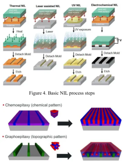
Nanoimprint lithography is an advanced nanofabrication method that is capable of high-throughput patterning of nanostructures with high resolution (down to the 5 nm regime). Because of the low cost, reduced process steps and high fidelity, NIL became an attractive technique for a wide range of applications. Nanoimprint lithography methods can be classified into four categories: thermal-NIL, UV-NIL, laser assisted NIL and electrochemical nanoimprints. The basic steps of NIL process is shown in Figure 4.
In thermal NIL, a fine film of a thermoplastic polymer (imprint resist) is deposited first by spin coating onto the substrate. The next step is to press the prefabricated mold with the substrate together under a certain pressure. Subsequent heating is used above the polymer's glass transition point to achieve the softened polymeric film. In the post thermal cooling process, the substrate is cooled down and mold is removed from it, while keeping the pattern resist on the substrate. Finally, an etching process is used to remove the resist residual layer. Youn et al. described a thermal roller NIL approach where the stamp is connected with two moveable springs through the pullers [39]. Replicating of ultra-precision micron scale structures can be achieved with this thermal roller imprinting process at the scan speed of 0.1–10 mm/s.
Figure 4. Basic NIL process steps
Figure 5. Schematic illustration of DSA processes [54] The laser assisted direct imprint (LADI) is a resistless
technique that does not require etching. With this technique, a single excimer laser pulse is exposed through the transparent quartz mold to melt a thin surface layer of silicon substrate. Then, the resulting liquid layer is embossed by the quartz mold. Finally, the mold is released after the substrate has cooled down. Various nanostructures with sub-10 nm resolution could be imprinted into silicon wafer using LADI with the embossing time below 250 ns. The capability of high resolution and high speed patterning, make the LADI as a promising technique for a variety of applications and it can be extended to other materials (polysilicon, Ge, and dielectrics) and processing techniques. Similarly, laser-assisted nanoimprint lithography (LAN) utilizes a single excimer laser pulse to melt the polymer. Then a fused quartz mold is used to pattern the nanostructures. This technique can be used in patterning various polymer films on a Si or quartz substrate with high fidelity over the entire mold area. Using LAN technique, the imprinting time could be less than 500 ns. The heating and expansion of the substrate and mold can also be reduced significantly so that better overlay alignment between the two can be achieved.
Electrochemical nanoimprinting is a resistless approach that uses a mold fabricated from a superionic conductor. In this process, a voltage is applied between the mold and the target substrate. Once the surfaces of the mold are in contact with the substrate, a current flows between them. The strong electric flux from the protrusive parts of the mold to the substrate results anodic oxidation of the substrate surface corresponding to the protrusive parts of the mold with the moisture present between the mold and the substrate. Subsequently, the substrate is etched to achieve the nanostructures like other methods.
NIL is the extremely simple process and offers a promising low cost alternative lithography technology with some other advantages such as high resolution, CDU and smaller LER. Nevertheless, some challenges have prohibited NIL from being adopted on a larger scale such as defectivity, contamination, throughput and overlay issues. Recently, significant improvement in the defect reduction on templates have been reported [40-42]. It has been revealed that overall process defectivity has been lessened by two orders of magnitude to 9 defects per cm2 [43]. Another key issue of NIL that should be realized is nano-defect management (NDM) technology which includes defect inspection of templates and imprinted wafer, the resist material innovation and the defect mitigation. These problems can be mitigated through intensive collaboration with various providers. Moreover, substantial studies are required on post etching resist defects and resist pattern etching resistance under sub-20 nm node [44]. Overlay improved by a factor of eight in several years and better than 5 nm 3 σ have been demonstrated [45]. One of the major influences of NIL technology is the capability of large area printing. Large area patterning with high density and high fidelity have been reported in the earlier reports [46-47]. It has been reported that throughput per imprint station improved fivefold to 10 wafers per hour [43]. For high resolution large area patterning, roll-type UV-NIL process with a
flexible transparent thin stamp has been proposed [48]. Last few years significant development of a high-speed and large-area roll-to-roll (RTR) and roll-to-plate (RTP) NIL apparatus for large area patterning of flexible substrates have been demonstrated [49-52]. The effect of the imprinting parameters such as temperature, loading force, aspect ratio and imprinting velocity on formability need to be realized. In addition, it is necessary to optimize the etching process carefully for high resolution replica fabrication. To accelerate this technology adoption, recently CEA-Leti and EV Group initiated a new program called INSPIRE to diversify the NIL applications beyond semiconductors [53]. Canon also designs nanoimprint lithography tools by collaborating with other vendors and the end users [45]. Nevertheless, NIL could offer its 3-D patterning capability for the advancement of 3-D chip technology. Because of its flexibility and ability to combine with other techniques, it has created huge opportunities for the future lithographic techniques for many others potential applications.
VI. DIRECTED SELF ASSEMBLY
Pattern defects is one of the critical issues to adopt DSA technology on semiconductor manufacturing. Missing and bridge hole are the typical defect types of DSA holes in physical guide. Researchers are also focusing on recognizing the factors that are responsible for the assembly defects (dislocations and line-period bridges). H. Pathangi, et al. presentedthe 14 nm half-pitch DSA line/space patterning into the Si substrate with reduced defectivity [55]. Moreover, to improve pattern quality, some experiments have been performed on various etch mask materials and etch process conditions [56]. LER is another challenge of DSA line patterns. For HVM industries the LER number should be about 10% of the target critical dimension (CD). Some methods have been proposed to improve the LER generated by PS-b-PMMA BCP [57]. Another issue of DSA of BCPs is the pattern density. Some pattern density enhancement approaches have been proposed including ‘thermal flow process’, ‘lift-off process,’ and ‘pattern trimming process’ [58-62]. By utilizing a low-topography resist prepattern ~5 teradot/in2 dot arrays with long-range order have been demonstrated [56]. Highly ordered patterns using PS-b-PDMS have been reported in some publications [63-64].
DSA can also integrates bottom-up self-assembly with top-down conventional lithography. The probable integration of DSA with ArF immersion photolithography for 16 nm line/space DRAM process scheduled in 2018 [65]. S. Morita et al. described a low-cost lithography process for making sub-15 nm pattern using DSA on nano-imprinting guide [66]. Development of several new processes have been reported such as CHIPS flow [67], LiNe process [68], SMARTTM process [69] and COOL process [70]. Recently, several application fields for DSA other than semiconductor device process such as flexible/transferable DSA technology utilizing chemically modified graphene (CMG) has been demonstrated [71-72]. However, further research will be required on perfect defect control, effective pattern transfer and nonplanar/flexible nanopatterning to make DSA capable of various commercial device manufacturing as a next-generation lithography solution.
VII. CONCLUSION
For many years, nanolithography technology has contributed to the advance in the nanomanufacturing industry and is influencing the future of nanoscience and technology. Through this article, an overall view of the potential next generation lithography techniques has been provided. Despite of the huge laboratory and commercial success, they are still suffering from various challenges and some of the key challenges have been discussed in this article. Finally, it can be said that the advancement in nanofabrication techniques is leading to technology revolutions in a broad area of applications.
REFERENCES
[1] J. Mulkens, et al., “Overlay and edge placement control strategies for the 7-nm node using EUV and ArF lithography,” Proc. SPIE 9422, 94221Q, 2015.
[2] D. Z Pan, L. Liebmann, B. Yu, X. Xu and Y. Lin, “Pushing multiple patterning in sub-10nm: are we ready?,” In: Proc. of the 52nd annual design automation conference; p. 1-6, 2015.
[3] International Technology Roadmap for Semiconductors (ITRS) 2015 Edition, 2015.
[4] B. Turkot, et al., “EUV progress toward HVM readiness,” Proc. SPIE 9776, 977602, 2016.
[5] Christian Wagner and Noreen Harned, “EUV lithography: Lithography gets extreme,” Nature Photonics 4, 24 – 26, 2010.
[6] A. Pirati, et al., “EUV lithography performance for manufacturing: status and outlook,” Proc. SPIE 9776, p. 97760A, 2016.
[7] M. Hori, et al., “Novel EUV resist development for sub-14 nm half pitch,” Proc. SPIE 9422, p. 94220P, 2015. [8] B. J. Lin, "Optical lithography with and without NGL for
single-digit nanometer nodes," Proc. SPIE 9426, 2015.
[9] Gemma Church. (2016, Jan.). The future of EUV
lithography. Electro Optics. Cambridge, UK. [Online]. Available: https://www.electrooptics.com/feature/future-euv-lithography
[10] Erik R. Hosler and Obert R., “Free-electron Lasers: Beyond EUV Lithography Insertion,” Wood II, p. 16. [11] EUV: Questions and answers (2013) ASML, Veldhoven,
Netherlands. [Online]. Available:
http://www.asml.com/asml/show.do?ctx=41905&rid=4190 6
[12] Hakaru Mizoguchi, et al., “Performance of new high-power HVM LPP-EUV source,” Proc. SPIE 9776, 2016. [13] E. R. Hosler, O. R. Wood, W. A. Barletta, P. J. S. Mangat,
and M. E. Preil, “Considerations for a free-electron laser-based extreme-ultraviolet lithography program,” Proc. SPIE 9422, p. 94220D, 2015.
[14] Yoichi Tanino, et al., “A Driver CO2 Laser Using Transverse-flow CO2 Laser Amplifers,” EUV Symposium 2013, Oct.6-10, 2013, Toyama.
[15] Tatyana Sizyuk and Ahmed Hassanein, “Revisiting Li as potential EUV source using dual-laser beam systems”, SPIE 9776-25, 2016.
[16] A. Hassanein and T. Sizyuk, “Pulse widths optimization of dual-beam laser systems for high-power EUV sources”, SPIE 9776-26, 2016.
[17] E. Buitrago, T. S. Kulmalax, R. Fallica and Y. Ekinci, “EUV lithography process challenges,” Frontiers of Nanoscience, Vol. 11, J. Hayton, Elsevier, 2016, p. 150. [18] T. Fujimori, T. Tsuchihashi and S. Minegishi, “Novel
ultra-high sensitive ‘metal resist’ for EUV lithography,” Proc. SPIE 9776-4, 2016.
[19] D. D. Simone, et al., “Novel metal containing resists for EUV lithography extendibility,” Proc. SPIE 9776-5, 2016. [20] Hideaki Tsubaki, et al., “Negative-tone imaging with EUV
exposure toward 13 nm hp,” Proc. SPIE 9776-8, 2016. [21] Seiichi Tagawa, et al., “The reaction mechanism and
patterning of photosensitized chemically amplified resists,” Proc. SPIE 9776-38, 2016.
[22] Kazuki Kasahara, et al., “Recent progress in nanoparticle photoresists development for EUV lithography,” Proc. SPIE 9776-3, 2016.
[23] W. Shibayama, et al., “Approach to hp-10 nm resolution by applying dry development rinse materials (DDRP) and materials (DDRM),” Proc. SPIE 9776-9, 2016.
[24] Yuichi Terashita, et al., “The reaction mechanism and patterning of photosensitized chemically amplified resists,” Proc. SPIE Advanced Lithography, 2016.
[25] Seiji Nagahara, et al., “Challenge toward breakage of RLS trade-off by new resists and processes for EUV lithography,” Proc. SPIE Advanced Lithography, 2016. [26] T. Nagai, et al., “Novel high sensitivity EUV photoresist
for sub-7 nm node,” Proc. SPIE Advanced Lithography, 2016.
[28] S. Tagawa, A. Oshima, C. Q. Dinh and S. Nishijima, “Fundamental aspects of a new process of high resist sensitization by the combination lithography of EB/EUV pattern exposure with UV flood exposure of photosensitized CAR and non-CAR,” Proc. SPIE Advanced Lithography, 2016.
[29] Jun Sung Chun, et al., “SEMATECH’s Cycles of learning test for EUV photoresist and its applications for process improvement,” Proc. SPIE 2014.
[30] Cecilia Montgomery, et al., “Novel processing approaches to enable EUV lithography toward high volume manufacturing”, International Symposium on EUVL, Washington DC, USA, 2014.
[31] W. Montgomery, J. S. Chun, M. Tittnich and M. Liehr, “The Patterning Center of Excellence (CoE): an evolving lithographic enablement model,” Proc. SPIE, 2015. [32] L. Girard, L. Marchetti and J. Kennon, “Fabrication of
EUVL micro-field exposure tools with 0.5 NA,” International Workshop on EUV Lithography, 2016. [33] P. Biagioni, et al., “Nanoantennas for visible and infrared
radiation,” Rep. Prog. Phys. 75, 2012, 024402, p. 40. [34] S. J. Lin, et al., “Multiple electron-beam direct-write
lithography: an overview,” Proc. SPIE 9777-3, 2016. [35] G. de Boer, et al., “MAPPER: Progress towards a
high-volume manufacturing system,” Proc. SPIE 8680, 2013. [36] E. Platzgummer, E. Klein, and H. Loeschner, “Electron
multi-beam technology for mask and wafer writing at 0.1 nm address grid,” Proc. SPIE 8680, 868001, 2013. [37] D. Lam, D. Liu, and T. Prescop, “E-beam direct write
(EBDW) as complementary lithography,” Proc. SPIE 7823, 78231C, 2010.
[38] Joe Nabity. (2017). Nanometer Pattern Generation System. JC Nabity Lithography Systems. USA. [Online]. Available: http://www.jcnabity.com/
[39] S. W. Youn, M. Ogiwara, H. Goto, M. Takahashi and R. Maeda, “Prototype development of a roller imprint system and its application to large area polymer replication for a microstructured optical device,” Journal of Materials Processing Technology, 202, 76–85, 2008.
[40] Michael C. Smayling, “Lithography alternatives meet design style reality: How do they "line" up?,” Proc. SPIE 9777, 977701, 2016.
[41] M. Hatano, et al., “NIL defect performance toward high volume mass production,” Proc. SPIE 9777, 977701, 2016. [42] H. Takeishi and S. Sreenivasan, “Nanoimprint system development and status for high volume semiconductor manufacturing,” Proc. SPIE 9423, 2015.
[43] M. Neisser and S. Wurm, “ITRS lithography roadmap: 2015 challenges,” Adv. Opt. Techn., 2015, 4(4), p. 235– 240.
[44] Tatsuhiko Higashiki, “Device fabrication using
nanoimprint lithography and challenges in nano-defect management,” Proc. SPIE 9777, 9777-4, 2016.
[45] T. Takashima, et al., “Nanoimprint system development and status for high-volume semiconductor manufacturing,” Proc. SPIE 9777, 9777-5, 2016.
[46] J. M. Keith, N. Gregory, B. Shufeng, and Y. C. Stephen, “Wafer-scale patterning of sub-40 nm diameter and high aspect ratio (more than 50:1) silicon pillar arrays by nanoimprint and etching,” Nanotechnology, no. 34, p. 345301, 2008.
[47] B. Cui,L. Clime, K. Li and T. Veres, “Fabrication of large area nanoprism arrays and their application for surface enhanced raman spectroscopy,” Nanotechnology, no. 14, p. 145302, 2008.
[48] J. Lee, S. Park, K. Choi, G. Kim, “Nano-scale patterning using the roll typed UV-nanoimprint lithography tool,” Microelectronic Engineering. 85, 861–865, 2008.
[49] S. H. Ahn, L. J. Guo, “Large-area roll and roll-to-plate Nanoimprint Lithography: A step toward
high-throughput application of continuous nanoimprinting,” ACS Nano. 3, p. 2304–2310, 2009.
[50] J. Taniguchi, H. Yoshikawa, G. Tazaki and T. Zento, J. Vac. Sci. Technol. B 30, 2012, 06FB07, 1-5.
[51] J. J. Dumond and H. Y. Low, J. Vac. Sci. Technol. B 30.1, 2012, 010801, 1-28.
[52] N. Kooy, K. Mohamed, L. T. Pin and O.S. Guan, “A review of roll-to-roll nanoimprint lithography,” Nanoscale Research Letters 9:320, 2014, 1-13.
[53] Hubert Teyssedre, et al., “200 mm wafer scale NIL process assessment for sub-micrometer CD uniformity with the SmartNIL process,” Proc. SPIE 9777-8, 2016.
[54] Courtesy of DOW Chemical Company.
[55] H. Pathangi, et al., “Block co-polymer contributions to the defectivity and roughness performance of the 14 nm half-pitch LiNe flow @ imec,” Proc. SPIE 9777-15, 2016. [56] S. Xiao, et al., “Pushing the limit of directed self-assembly
and double patterning to 4 nm half-pitch and beyond,” Proc. SPIE 9777-15, 2016.
[57] M. Muramatsu, et al., “Pattern fidelity improvement of
chemo-epitaxy DSA process for high-volume
manufacturing,” Proc. SPIE 9777-14, 2016.
[58] S.H. Park, et al., “Block copolymer multiple patterning integrated with conventional ArF lithography,” Soft Matter 6, 2010, 120.
[59] J. Y. Cheng, et al., “Simple and versatile methods to integrate Directed Self-Assembly with optical lithography using a polarity-switched photoresist,” ACS Nano 4, 2010, p. 4815-4823.
[60] M. Somervell, et al. SPIE Proc. 8325, 2012, 83251G-1. [61] H. S. Moon, et al., “Large-area, highly oriented lamellar
block copolymer nanopatterning directed by
graphoepitaxially assembled cylinder nanopatterns,” J. Mater. Chem. 22, 2012, 6307.
[62] S. J. Jeong and S. O. Kim, “Ultralarge-area block copolymer lithography via soft graphoepitaxy,” Journal of Material Chemistry, 21, 5856, 2011.
[63] Y. S. Jung, et al., “A path to ultranarrow patterns using self-assembled lithography,” Nano Lett. 10, 2010, p. 1000-1005.
[64] J. W. Jeong, et al., “Highly tunable self-assembled
nanostructures from a poly
(2-vinylpyridine-b-dimethylsiloxane) block copolymer,” Nano Lett. 11, 2011, p. 4095-101.
[65] International Technology Roadmap for Semiconductors (ITRS) 2012 Edition, Semiconductor Industry Association, San Jose, CA, 2012.
[66] S. Morita, et al., “Sub-15nm patterning technology using directed self-assembly on nanoimprinting guide,” Proc. SPIE 9777-19, 2016.
[67] A. Singh, et al., “Patterning sub-25nm half-pitch hexagonal arrays of contact holes with chemo-epitaxial DSA guided by ArFi pre-patterns,” Proc. SPIE 9425, 94250X, 2015. [68] C-C. Liu, et al., “Chemical Patterns for Directed
Self-Assembly of Lamellae-Forming Block Copolymers with Density Multiplication of Features,” Macromolecules, 46(4), p. 1415-1424, 2013.
[69] J. Kim, et al., “SMARTTM process for directed block co-polymer self-assembly,” J. Photoco-polymer Sci. Technol., 26(5), p. 573-579, 2013.
[70] Y. Seino, et al., Proc. SPIE, 9423, 9423-41, 2015. [71] B. H. Kim, et al., “Surface Energy Modification by
Spin-Cast, Large-Area Graphene Film for Block Copolymer Lithography,” ACS Nano 4, 2010, p. 5464-5470.
![Figure 1. Schematic of an EUVL system [5]](https://thumb-us.123doks.com/thumbv2/123dok_us/1457681.98457/2.595.333.514.237.337/figure-schematic-an-euvl-system.webp)
![Figure 3. The process steps of EBL and FIBL system [33]](https://thumb-us.123doks.com/thumbv2/123dok_us/1457681.98457/3.595.74.272.529.736/figure-process-steps-ebl-fibl.webp)