16 Bit Unsigned Multiplier Using Proposed CSLA
Praveen B S1, Manjunath Badiger2
1
Student, 2Assistant Professor, Dept. Of ECE, SDIT Mangalore (India)
Abstract--This project deals with the comparison of the VLSI design of the conventional carry select adder (CSLA) based 16-bit unsigned integer multiplier and the VLSI design of the proposed carry select adder (CSLA) based 16-bit unsigned integer multiplier. Both the VLSI design of multiplier multiplies two 16-bit unsigned integer values and gives a product term of 32-bit Values. The Conventional CSLA based multiplier uses the delay time of 12.845ns for performing multiplication operation where as in proposed CSLA Based multiplier also uses nearly the same delay time for multiplication operation. But the area needed for CLAA multiplier is reduced to 30 % by the CSLA based multiplier to complete the multiplication operation. These multipliers are implemented using Xilinx 14.5.
Keywords- CSLA, Delay, Area, Multiplier, VHDL Modeling & Simulation
I. INTRODUCTION
Carry select adder is one of the fastest adders used in many dsp’s, to perform fast arithmetic functions. Sum and carry are calculated by assuming input carry as 1 and 0 prior to input carry comes .When the actual carry input arrives , the actual calculated values of sum and carry are selected using a multiplexer. Low-Power, area-efficient, and high-performance VLSI systems are increasingly used in portable and mobile devices, multi-standard wireless receivers, and biomedical instrumentation. An adder is the main component of an arithmetic unit. A complex digital signal processing (DSP) system involves several adders. An efficient adder design essentially improves the performance of a complex DSP system. A ripple carry adder (RCA) uses a simple design, but carry propagation delay (CPD) is the main concern in this adder.Carry look-ahead and carry select (CS) methods have been suggested to reduce the CPD of adders. A conventional carry select adder (CSLA) is an RCA–RCA configuration that generates a pair of sum words and output carry bits corresponding the anticipated input-carry (cin =0 and 1) and selects one out of each pair for final-sum and final-output-carry. A conventional CSLA has less CPD than an RCA, but the design is not attractive since it uses a dual RCA. Few attempts have been made to avoid dual use of RCA in CSLA design. Digital computer arithmetic is an aspect of logic design with the objective of developing appropriate algorithms in order to achieve an efficient utilization of the available hardware. The basic operations are addition, subtraction, multiplication and division. In this, we are going to deal with the operation of additions implemented to the operation of multiplication. The repeated form of the addition operations and shifting results in the multiplication operations. Given that the hardware can only perform a relatively simple and primitive set of Boolean operations, arithmetic operations are based on a hierarchy of operations that are built upon the simple ones. In VLSI designs, speed, power and chip area are the most often used measures for determining the performance and efficiency of the VLSI architecture. Multiplications and additions are most widely and more often used arithmetic computations performed in all digital signal processing applications. Addition is a fundamental operation for any digital multiplication. A fast, area efficient and accurate operation of a digital system is greatly influenced by the performance of the resident adders. Adders are also very important component in digital systems because of their extensive use in these systems. In this project we are going to compare the performance of different adders implemented to the multipliers based on area and time needed for calculation. On comparison with the conventional carry select adder (CSLA) based multiplier the area of calculation of the proposed carry select adder (CSLA) based multiplier is smaller and better with nearly same delay time. Here we are dealing with the comparison in the bit range of n*n (16*16) as input and 2n (32) bit output. Hence, to design a better architecture the basic adder blocks must have reduced delay time consumption and area efficient architectures. The demand is of DSP style systems for both less delay time and less area requirement for designing the systems. Our interest is in the basic building blocks of arithmetic circuits that dominate in DSP applications, VLSI architectures, computer applications and where ever reduced area computation is needed.
conventional and BEC-based CSLAs of [6] by suitable logic expressions. The main objective of this study is to identify redundant logic operations and data dependence. Accordingly, we remove all redundant logic operations and sequence logic operations based on their data dependence. Suppose two n-bit operands are added in the conventional CSLA, then RCA-1 and RCA-2 generate n-bit sum (s0 and s1) and output-carry (c0 out and c1 out) corresponding to input-carry (cin = 0 and cin = 1), respectively.
Fig. 1.(a) Conventional CSLA; n is the input operand bit-width. (b) The logic operations of the RCA is shown in split form, where HSG, HCG, FSG, and FCG represent half-sum generation, half-carry generation, full-sum generation, and full-carry generation, respectively.
Logic expressions of RCA-1 and RCA-2 of the SCG unit of the n-bit CSLA are given as S00 (i) =A(i) Xor B(i) , C00(i) = A(i) and B(i) (1a)
S01 (i) =S00 (i) Xor C01 (i −1) (1b)
C01 (i) =C00 (i) + S00(i) andC01(i −1) ,C0out=C01(n −1) (1c)
S10 (i) =A(i) Xor B(i) C10(i) = A(i) and B(i) (2a)
S11 (i) =S10 (i) Xor C11(i −1) (2b)
C11 (i) =C10 (i) +S10 (i) and c11 (i −1), c1out=c11(n −1) (2c) Where C01 (−1) = 0, c11(−1) = 1, and 0 ≤ i ≤ n −1.
[image:3.612.197.452.145.258.2]As shown in equation (1a) to (1c) and (2a) to(2c) the logic expression of{ S00(i),C00(i)} is identical to that of {S10(i),C10(i)}. These redundant logic expression can be removed to have an optimized design for RCA2 in which the HSG and HCG of RCA1 is shared to construct RCA2.
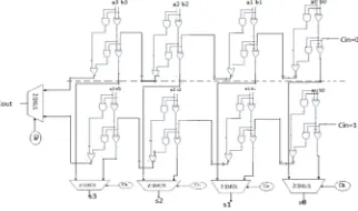
Figure 2:-Gate Level Design Of Conventional CSLA The proposed logic formulation for the CSLA is given as
s0(i)=A(i)XORB(i),c0(i)=A(i)andB(i) (3a) c01(i)=c01(i-1)ands0(i)+c0(i) for c01(0)= 0 (3b) c11(i)=c1(i-1)ands0(i)+c0(i)forc11(0) = 1 (3c)
c(i)=c01(i)if(cin= 0) (3d)
c(i)=c11(i)if(cin= 1) (3e)
cout=c(n−1) (3f)
s(0) =s0(0)XORcin, s(i)=s0(i) XOR c(i − 1) (3g)
[image:3.612.221.382.469.564.2]Figure3:-Gate Level Design of Proposed CSLA
The selected carry word is added with the half-sum (s0) to generate the final-sum (s). Using this method, one can have three design advantages: 1) Calculation of s01 is avoided in the SCG unit; 2) the n-bit select unit is required instead of the (n + 1) bit; and 3) small output-carry delay. All these features result in an area–delay and energy-efficient design for the CSLA.We have removed all the redundant logic operations of (1a)–(1c) and (2a)–(2c) and rearranged logic expressions of (3a)–(3c) and (3d)–(3g) based on their dependence
III. MUL TIPLTER FOR UNSIGNED DATA
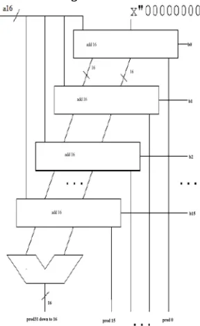
[image:4.612.231.375.348.582.2]Multiplication involves the generation of partial products, one for each digit in the multiplier, as in Figure3.These partial products are then summed to produce the final product. The multiplication of two n-bit binary integers results in a product of up to 2n bits in length [2] We used the following algorithm to implement the multiplication operation for unsigned data. We used the following algorithm to implement the multiplication operation for unsigned data.
Figure 4:- A partial schematic of the multiplier
IV. MULTIPLTER DESIGN USING CSLA
The multiplication of two n-bit binary integers results in a product of up to 2n bits in length [2]. Let the product register size be 32 bits. Let the multiplicand registers size be 16 bits. Store the multiplier in the least significant half of the product register. Clear the most significant half of the product register.
Figure 5:-CSLA Multiplier of two n-bit values.
V. VHDL SIMULATIONS
The VHDL simulation of the two multipliers is presented in this section. In this, waveforms, timing Diagrams and the design summary for both the CSLAs based multipliers are shown in the figures. The VHDL code for both multipliers, using conventional CSLA and proposed CSLA, are generated .The multipliers use two 32-bit values. Under the worst case, the multiplier with a conventional carry select adder uses time == 3.150 ns, while the multiplier with the proposed carry select adder uses time 5.356 ns.
VI. CONCLUSION
A design and implementation of a VHDL- based 16 bit unsigned multiplier with both CSLAs was presented. VHDL, a Very High Speed Integrated Circuit Hardware Description Language, was used to model and simulate this multiplier. Using proposed CSLA improves the overall performance of the multiplier. Thus a 30 % area and delay reduction is possible with the use of the proposed CSLA based 16 bit unsigned multiplier than conventional CSLA based 16 bit unsigned multiplier.
VII. FUTURE WORK
This 16 bit multiplier can be further extended to 32 and 64 bit multiplier. 128 bit multiplier using the proposed method for multiplication operation can be done as future work.
REFERENCES
[1] K. K. Parhi, VLSI Digital Signal Processing. New York, NY, USA:Wiley, 1998. applications,” Annu. Rev. Biomed. Eng., vol. 10, pp. 247–274, Aug. 2008. [2] O. J. Bedrij, “Carry-select adder,” IRE Trans. Electron. Computer.,vol. EC-11, no. 3, pp. 340–344, Jun. 1962.
[3] Y. Kim and L.-S. Kim, “64-bit carry-select adder with reduced area,” Electron.Lett., vol. 37, no. 10, pp. 614–615, May 2001.
[4] B. Ramkumar and H.M. Kittur, “Low-power and area-efficient carry-select adder,” IEEE Trans. Very Large Scale Integr. (VLSI) Syst., vol. 20, no. 2, pp. 371– 375, Feb. 2012
[5] V.Vijayalakshmi ‘Design and Implementation of 32 bit Unsigned Multiplier using CLAA and CSLA’ National conference in SBCEC, Jan, 2013. [6] S. Brown and Z. Vranesic, Fundamentals of Digital Logic with VHDL Design, 2nd ed., McGraw-Hill Higher Education, USA, 2005.
[7] J. R. Armstrong and F.G. Gray, VHDL Design Representation and Synthesis, 2nd ed. , Prentice Hall, USA, 2000. ISBN: 0-13-021670-4. [8] Z. Navabi, VHDL Modular Design and Synthesis of Cores and Systems, 3rd ed., McGraw-Hill Professional, USA, 2007.
[9] P. C. H. Meier, R. A. Rutenbar and L. R. Carley, "Exploring Multiplier Architecture and Layout for low Power", CIC'96, 1996.
Design Width(n) Delay(ns) Area(slices)
Conventional CSLA
16 5.356 30
Proposed CSLA