Abstract-. The design objective is to implement a Low power, High speed and High resolution Flash ADC with increased sampling rate. To make this possible the blocks of ADC are analyzed. The resistive ladder, comparator block, encoder block are the major modules of flash ADC. Firstly, the comparator block is designed so that it consumes low power. A NMOS latch based, PMOS LATCH based and a Strong ARM Latch based comparators were designed separately. A comparative analysis is made with the comparator designs. Comparators in the design is reduced to half by using time domain interpolation. Then a reference subtraction block is designed to generate the subtraction value of voltages easily and its given as input to comparator. Then a more efficient and low power consuming fat tree encoder is designed. Once all the blocks were ready, a 8 bit Flash Analog to Digital Converter was designed using 90nm CMOS technology and all the parameters such as sampling rate, power consumption, resolution were obtained and compared with other works.
I. INTRODUCTION
Fields of ADC usage include medical, radar, data acquisition.
Modules of general flash ADC • Reference r-ladder • Voltage input
• Comparator
• Encoder logic
To make the Flash ADC more efficient, we have dealt with some basic key issues of Flash ADC such as speed, performance, area and power consumption by using some techniques.
Fig. 1. Flash ADC Block
II. PROPOSED SYSTEM
Revised Manuscript Received on September 10, 2019.
[image:1.595.313.561.169.518.2]Dr. Deepa Jose, Associate Professor, Department of ECE, KCG College of Technology, Chennai, Tamilnadu, India.
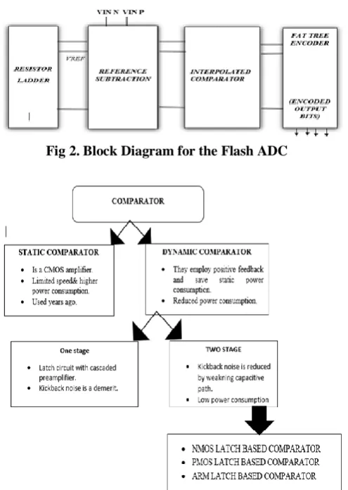
Fig 2. Block Diagram for the Flash ADC
Fig 3. Flow for the Comparitive Analysis of the Comparator
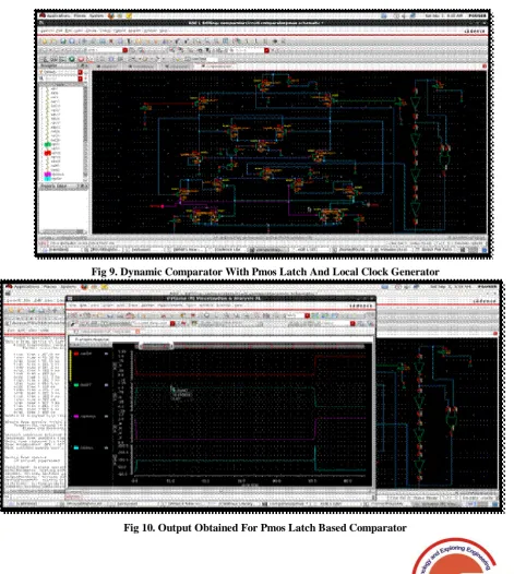
Design Of Two Stage Dyamnic Comparator With Nmos Latch
Fig 4. Twostage Dynamic Comparator with NMOS Latch
A 1000 Mhz Low Power And High Speed 8-Bit
Flash ADC Architecture using 90nm Cmos
Technology
To set the gain higher, the transistor M3,4 are chosen to have a appropriate size. But the delay parameters are
[image:2.595.125.487.55.762.2]controlled by offset which can be overcome by a pmos latch.
Fig 5. Schematic Of NMOS Latch Based Comparator In Cadence
Fig 6. Output Obtained For Precharge And Evaluation
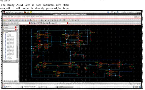
Design Of Two Stage Dyamnic Comparator With Pmos Latch
[image:3.595.154.445.75.220.2][image:3.595.59.531.254.780.2]
Fig 8. Twostage dynamic comparator with pmos latch and local clock generator.
Fig 9. Dynamic Comparator With Pmos Latch And Local Clock Generator
A optimum delay is being defined in this type of comparator.It consists of a preamplifier stage where a local
[image:4.595.51.537.50.329.2]generator is designed which plays a major role.In the evaluation phase a predetermined delay is defined.
Fig 11. Power Consumption Of Design Based On Pmos Latch
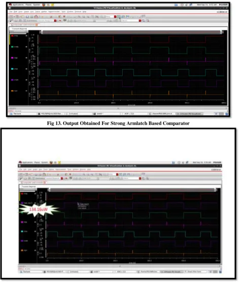
Design Of Two Stage Dyamnic Comparator With Strong Arm Latch
The strong ARM latch is does consumes zero static power,rail to rail output is directly produced,the input
referred offset arises from one differential pair.This makes the Strong ARM latch popular.
[image:4.595.54.549.372.681.2]In the reset phase,clock is low and the nodes A,B,C,D is precharged to vdd where transistor M2 is off.In the next
[image:5.595.69.541.86.642.2]phase-amplification mode,clock goes high,transistor M1 and M2 are on.This phase provides voltage gain.
[image:5.595.79.526.89.335.2]Fig 13. Output Obtained For Strong Armlatch Based Comparator
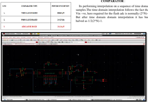
Comparitive Analysis Of Powerconsumption Among The Comparators
Since ARMLATCH BASED comparator is consuming the least performance and has improved speed,We prefer this comparator for our proposed ADC design.
TABLE 1.
Thus , We prefer the Strong ARM Latch comparator(Lowest power consuming) in the proposed Flash ADC design
III. TIME DOMAIN INTERPOLATION OF THE COMPARATOR :
[image:6.595.57.541.125.458.2]Its performing interpolation on a sequence of time domain samples.The time-domain interpolation follows the fact that, Vin +ve, here required for the flash adc is normally (2^N)-1. But after time domain domain interpolation it has been halved as 1/2(2^N)-1.
Fig 15. Time Domain Interpolation Unit In Cadence
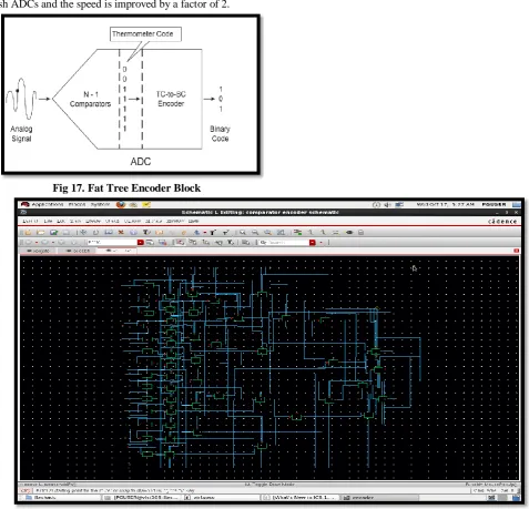
IV. FAT TREE ENCODER & RESULTS
[image:7.595.59.537.81.540.2]Its preferred that is highly suitable for the ultrahigh speed flash ADCs and the speed is improved by a factor of 2.
Fig 17. Fat Tree Encoder Block
Fig 18. Implementation Of Encoder In Cadence
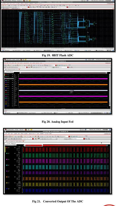
V. PROPOSED 8BIT FLASH ADC
The Reference generated is subtracted with the voltage input and is fed to the comparator.The output generated from the comparator, which is of digital bits and its encoded
Fig 19. 8BIT Flash ADC
Fig 20. Analog Input Fed
[image:8.595.108.500.56.752.2]
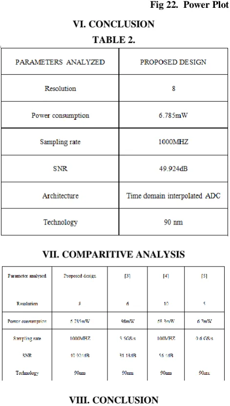
Fig 22. Power Plot For The Designed ADC
VI. CONCLUSION TABLE 2.
VII. COMPARITIVE ANALYSIS
VIII. CONCLUSION
This research paper analyzes the Flash ADC the parameters transient response, power consumed, sampling rate, resolution and SNR using Cadence EDA. And also we
circuit provides higher SNR. In future we analyse by using different technology (i.e 45nm, 65nm).
IX. REFERENCES
1. Kenichi Ohhata , Member, IEEE, Daiki Hayakawa, Kenji
Sewaki, Kento Imayanagida,Kouki Ueno, Yuuki Sonoda, and Kenichiro Muroya ,”A 900-MHz, 3.5-mW, 8-bit Pipelined Subranging ADC Combining Flash ADC and TDC”, 1063-8210 © 2018 IEEE.
2. Hadi Aghabeigi,mehdi Jafaripanah, Tafresh university,
Tafresh, Markazi, Iran,”High Speed Low Power Voltage comparator In 0.18um CMOS Process For Flash ADC” ,978-1-5386-2640-5/17 © 2017 IEEE.
3. Kazuaki Deguchi, Naoko Suwa, Masao Ito, Toshio
Kumamoto and Takahiro Miki Advanced Alog Technology Division, Renesas Tehnology Corporation 4-1, Miizhara, Itami, Hyogo, 664-0005, Japan, E-mail: DegueliKazutkilrrnesas.com,”A 6-bit 3.5-GS/s 0.9-V 98-mW Flash ADC in 90nm CMOS”,978-4f-900784-04f-8 2007 Symposium on VLSI Circuits Digest of Technical Papers.
4. Ko-Chi Kuo ,Department of Computer and Science
Engineering,National SunYetsenUniversity,Kaohsiung, Taiwan, Email: [email protected], ”A 1.2V 10 bits 100-MS/s Analog-to-Digital Converter with a 8-stage pipeline and a 2 bits flash ADC”,ISBN 978-1-5090-4897-7,IEEE-ICASI 2017.
5. Jonathan E. Proesel and Lawrence T. Pileggi, “A 0.6-1 V
![[A letter on] [t]he Sustainable Development Commission Scotland’s response to the Scottish Government consultation on a Scottish Climate Change Bill](data:image/gif;base64,R0lGODlhAQABAIAAAP///wAAACH5BAEAAAAALAAAAAABAAEAAAICRAEAOw==)