Abstract: In this paper, we designed complex gate which is having very good performance in terms of delay. This is achieved by increasing threshold voltage. The reduced delay and its percentage variation with respect to threshold voltage is shown below in the result analysis. Increasing of threshold voltage not only reduces delay but indirectly reduces leakage power consumption. Now-a-days Efficient Complex Gate using 45nm technology is preferable because of its delay and power.
Keywords : Complex gate, Low Power, Delay , DSP, VLSI.
I. INTRODUCTION
In today’s environment, to implement real time applications like video compression, graphics, gaming etc. designers have been primarily focused on speed optimization. For designing all these real time applications with semiconductor IC’s, one has to focus for portability of the device where packaging is done with low power consumption. Reduction of power consumption in VLSI Systems plays a vital role because it maximizes the run time. Power consumption also effects on delay, chip density, size and life of battery[1].
Power dissipation in VLSI systems are essentially three types i.e, dynamic power dissipation, Short circuit current, Ileakage. In logic gates, charge and discharge of load capacitance creates dynamic power consumption whereas shorting of P,N Branches forms logic gate changes state momentarily results in cut off dissemination and leakage current occurs when the system is not powered or in Standby mode[2].To overcome this problem, Researchers focused on components which consumes low power and design techniques because for every 100 C rise in temperature, silicon failure is doubled in devices with higher power consumption. Power is a supernatural improvement which assembled significance with the advancements of profound submicron hubs and more current VLSI nanometer innovations[3] .
We have designed efficient complex gate of Boolean expression
---(1)
Revised Manuscript Received on December 05, 2019.
Sudhakar Alluri is with the electronics and communication engineering Department, CMR Institute of Technology, Hyderabad, T.S, India, e-mail: [email protected].
D.Mamatha, is with the ECE, CMR Institute of Technology, Hyderabad, TS, India, e-mail: dyavamamatha @gmail.com.
K.Mounika, is with the ECE, CMR Institute of Technology, Hyderabad, TS, India, e-mail: mounikareddy1105 @gmail.com.
The above equation-1is implemented with 45nm technology in cadence tool which is having low power dissipation, area and delay.
II. LITERATURE SURVEY 2.1 Complex Gates
Complex Gates are widely used in chip design of VLSI circuits. The advantage of this complex gates are they can be designed in very efficient manner based of powerful combinations of series and parallel connection of transistors[12].
2.2 45Nm Technology
In 45nm technology, bulk manufacturing is done by transistors with high-k+metal which is of dielectric material. Double patterning method is used in fate patterning.
There are two main reasons using this gate material. One it improves the stress enhancement integration. This is done by transistors with double metal-gate + high-k dielectric. The second one is the shifting to 45nm technology node pitches from 193nm dry lithography. These two features improved transistor performance for leading industry.
III. SOURCES OF POWER DISSIPATION Any system either it may electrical or electronic the rate of power dissipation in a particular interval of time is called power dissipation. They are named as peak and average power dissipation. The maximum momentary power for a given time is called maximum power. It mainly effects reliability of the device by producing glitches in the circuit. This indirectly makes malfunctioning of the circuit.
Next one is average power which effects coolness and the method of packing of the device. The total or net power dissipation is given by the below expression [2].
P(t)=V(t)*I(t)……….. (2) Where V(t) is the biasing voltage provided by power supply and I(t) is the instantaneous current. In general power can be minimized by concentrating on average or max. instantaneous power. As we already discussed earlier, the total power dissipation of Complementary MOS logic circuits are leakage, dynamic and short circuit power. Hence, total power distraction of Complementary Metal Oxide Semiconductor circuit is as follows.
Ptotal=Pswitching+Pshort+Pleakage Pswitching=α CLV2f
Pshort=ταV Ishort Pleakage=VIleakage
CL can be the capacitance connected at the output which acts as capacitance of load, f can be Switching Frequency ,V can be Voltage, α can be time
response,
Design of Efficient Complex Gate using 45nm
Technology
Fig 1(a):High capacitance load. Fig1(b):Low capacitance load
leakage power dissipation
[image:2.595.308.542.53.222.2]The above Fig1(a) & Fig1(b) shows that the high and low capacitance of load leakage power dissipation in reverse bias. A reverse bias current is formed due to leakage due to subthreshold, tunneling of gate oxide terminal, substrate of deviceand the diffused region. These biased current and Ileakage causes static power[2][3].
Fig 2 shows the power dissipation due to shorting MOS branches and it is observed from experimental results that this power is reduced by nano technology. In our paper, we reduce this power by introducing 45 nm technology for complex gate.
Fig 3.Dynamic power due to load capacitance Fig 3 shows that the charge and discharge of load capacitance creates dynamic power. The dynamic power consumption is higher as compared to other power consumptions[4]. Hence, reduction of this dynamic power plays a vital role in VLSI circuits.
3.1 Threshold Voltage and Delay
The minimum amount of voltage required to make transistor ON is called Threshold voltage.
Threshold Voltage varies with different parameters like amount of Doping, Thickness of oxide and Source to Body Voltage (Body bias voltage)[6].
[image:2.595.65.283.55.162.2]The amount of time required time for the circuit to change the output from either high-low or low-high is called as Delay time.It is generally 50% of input–output switching time which is shown in below figure.
Fig 4: Threshold voltage
Delay time is expressed as Ta=(Tphl+Tplh)
2 3.2 Threshold Voltage Vs Delay
To overcome the problem of power consumed, the delay should be reduced. This is achieved by hopping of threshold voltage. The method of threshold voltage variation dynamically on a load is called threshold voltage hopping(i.e, V<sub>TH</sub>-hopping)[7].
3.3 Area Estimation:
Area required to implement any given logic by the product of horizontal and vertical dimensions.
III. METHODOLOGY
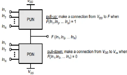
Complementary logic gate is a combination of network consisting of 2 sub systems which are pull-up and pull-down networks. They can also be named as PUN and PDN Networks. Below figure shows the logic gate with N possible inputs. Here all the N inputs are to be connected to both PUN and PDN networks. The pull-up network connected between Vdd and output and pull-down is connected between output and ground. If the output is connected to Vdd then output becomes logic1(i.e, High). If the output is connected to Vss then output becomes logic0(i.e, Low)[5].A CMOS logic can be designed in an exclusive manner in such a way that only one of the network that may be pull-up or pull-down will conducts in steady state. A short circuit path will be created between Vdd & output for high logic of input and for low logic of input a shorted path will takes place between Vss and Gnd.
Fig 5:CMOS with Pull-up &Pull-down systems.
[image:2.595.54.285.288.401.2] [image:2.595.102.234.468.590.2] [image:2.595.329.541.552.677.2]IV. IMPLEMENTATIONOFCMOSCOMPLEX GATE
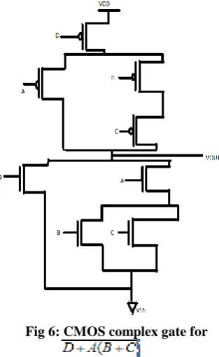
[image:3.595.95.252.261.517.2]Development of any other logic using CMOS Inverters: Once if we have designed CMOS inverter, any logic can be implemented by it. The logic will be implemented by putting the logic expression in sum of product form i.e., with inversion at the output which is indicated by the bar at the top of the logic expression[6].There are two main principles in the logic implementation using PMOS and NMOS transistors for CMOS design style. They are the following one[5][7]. In pull up network, if we have AND(i.e. dot symbol) logic, PMOS transistors are connected in parallel whereas for OR(i.e.,+ symbol) transistors are connected in series. In pull down network, if we have AND(i.e. dot symbol) logic, NMOS transistors are connected in series whereas for OR(i.e.,+ symbol) transistors are connected in parallel. 5.1 CMOS COMPLEX GATE:
Fig 6: CMOS complex gate for
From the above circuit A,B&C,B are inputs and Y is the output. Here we can check the output for our logic using different inputs are explained below[8].
If A=B=C=D=0, all the PMOS gates (pull up gates) are in ON condition because PMOS will be in ON state for logic 0 input then all the PMOS circuits are allow the Vdd to pass through it. In pull-down network all the NMOS circuits are OFF for the logic 0 condition, so the Vdd which is passing through the pull-up network will not allowed by the pull down network, then total power passed to the output side through the pull up network then output will become high(I.e, Y=1)[9].
If A=0,B=1,C=0,D=0, here in pull up network A,C,D transistors are ON for logic 0 as input and B transistor is OFF for logic 1 as input[9][8]. In pull down network only B transistor is ON condition as logic 1 as the input. Here in pull up network the Vdd will pass through the transistors D ,A to the output Y, here no short circuit will established through the transistor B (B is off condition).In pull down network only transistor B is in ON condition but it is connected parallel to the transistor C series to the transistor A and here A is in OFF
condition, so no short circuit path is established to the ground then output will become high(I.e, Y=1).
If A=0,B=0,C=0,D=1, In pull up network transistors A,B and C are ON and D is OFF and in pull down network transistors A,B and C are OFF & D is ON then output Y is 0. If A=0,B=0,C=1,D=0, In pull up network transistors A,B and D are On and C is Off and in pull down network transistors A,B&D are OFF and C is ON then output Y is 1. If A=B=0,C=D=1, In pull up network transistors A,B are ON and C,D are OFF and In pull down network transistors A,B are OFF and C,D are ON then output Y is 0.
If A=0,B=1,C=0,D=1, In pull up network transistors A,C are ON and B,D are OFF and In pull down network transistors A,C are OFF and B,D are ON then output Y is 0.
If A=0,B=1,C=1,D=0, In pull up network transistors A and D are On and B&C are Off and in pull down network transistors A,D are OFF and C,B are ON then output Y is 1. If A=0,B=1,C=1,D=1, In pull up network transistors A is ON and B,C,D are OFF and In pull down network transistors A is OFF and B,C,D are ON then output Y is 0.
If A=1,B=C=D=0, In pull up network transistors A is OFF and B,C,D are ON and In pull down network transistors A is ON and B,C,D are OFF then output Y is 1.
If A=D=1,B=C=0,, In pull up network transistors B,C are On and A,D are Off and In pull down network transistors A&D are On and C&B are Off then output Y is 0.
If A=1,B=0,C=1,D=0, In pull up network transistors B,D are ON and A,C are OFF and In pull down network transistors A,C are ON and B,D are OFF then output Y is 0.
If A=1,B=0,C=1,D=1, In pull up network transistors A,C,D are OFF and B is ON and In pull down network transistors A,C,D are ON and B is OFF then output Y is 0.
If A=0,B=1,C=0,D=0, In pull up network transistors A,C,D are ON and B is OFF and In pull down network transistors A,C,D are OFF and B is ON then output Y is 1.
If A=1,B=1,C=0,D=1, In pull up network transistors A,B,D are OFF and C is ON and In pull down network Transistors A,B&D are On while C is Off then output Y is 0.
If A=1,B=1,C=1,D=0, In pull up network Transistors A,B&C are Off and D is On and in pull down network Transistors A,B&C are ON & D is Off then output Y is 0. If A=1,B=1,C=1,D=1, In pull up network all Transistors A,B,C&D are Off while In pull down network Transistors a,b,c&d are On then output Y is 0.
V. SOFTWAREUSED
The designed complex gate using CMOS logic have been implemented in cadence virtuoso tool in 45nm technology[11]. Cadence provides ease of environment for characterization and validation solutions, simulation, design. It also provide automation of layout. Cadence also provides characteristics like, power analysis, delay, area etc.
VI. RESULTS
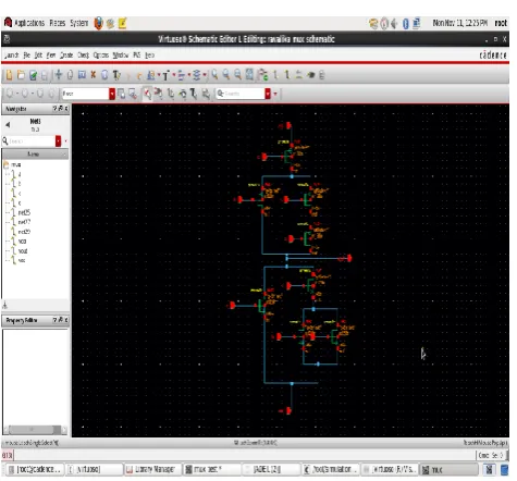
[image:4.595.311.541.84.198.2]Fig 7 : Schematic Implementation of CMOS Complex gate with expression of equation-(1) in cadence The above complex circuit is designed in cadence tool with the logic of equation-(1) as shown above.It has 4 inputs and single output.We can generate different outputs by changing input combinations.
[image:4.595.307.547.275.496.2]Fig 8 :Generation of symbol for Complex Gate The above figure shows the schematic of the complex logic for equation-(1) generated from the transistor level diagram using cadence tool.
Fig 9:Test circuit of Complex Gate
The above figure shows the schematic of the complex gate, Here we can test the circuit by applying input pulse ,supply
and ground.We can observe the performance of the circuit by giving different voltages.
Fig 10 : Simulation of test circuit
For simulation select inputs and outputs of test circuit and click on run then we will get the below shown output waveforms.
VII. OUTPUTWAVEFORMS
[image:4.595.52.289.368.542.2]Fig 11:Outputs waveforms of Complex gate The above figure represents the output signals for the corresponding input signals in different colours where blue represents input signal D, pink represents input signal C, green represents input signal B, violet represents input signal A and violet represents output signal.
Table 1:Comparison of delay with respect to threshold voltage
S.No.
Threshold
voltage(V) Delay(ps)
1. 0.1 113.3
2. 0.2 102.4
3. 0.3 94.92
4. 0.4 87.76
5. 0.5 80.72
6. 0.6 73.18
7. 0.7 66.84
8. 0.8 59.96
9. 0.9 53.12
[image:4.595.57.281.596.751.2]The above table shows the values of Threshold voltage Vs delay for the logic of equation-(1), Here we can observe that the delay is decreasing by increasing the Threshold voltage.By decreasing the delay automatically the power and area will also decreases.
Fig 10:Comparison of threshold voltage voltage and delay Fig 10 represents delay reduced with respect to threshold voltages.The delay reduced is not uniform over all the threshold voltages.The delay reduction is normally between from 6-8 threshold voltage to another threshold voltage.
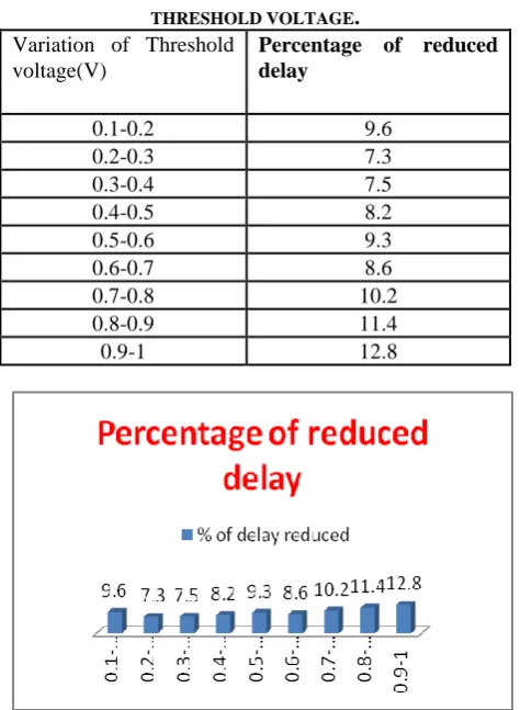
TABLE 2: % OF DELAY REDUCED WITH RESPECT TO THRESHOLD VOLTAGE.
Variation of Threshold voltage(V)
Percentage of reduced delay
0.1-0.2 9.6
0.2-0.3 7.3
0.3-0.4 7.5
0.4-0.5 8.2
0.5-0.6 9.3
0.6-0.7 8.6
0.7-0.8 10.2
0.8-0.9 11.4
0.9-1 12.8
fig 11 :% of delay reduced with respect to threshold voltage
VIII. CONCLUSION
In this paper, we designed complex gate which is having very good performance in terms of delay. This is achieved by increasing threshold voltage. The reduced delay and its percentage variation with respect to threshold voltage are shown below in the result analysis. Increasing of threshold voltage not only reduces delay but indirectly reduces leakage power consumption. Now-a-days Efficient Complex Gate using 45nm technology is preferable because of its delay and power.
REFERENCES
1. Sridhar Abburi and Rapoul Anil Kumar, ―Design Methodologies and Strategies for Low Power VLSI‖, International Journal for Modern Trends in Science and Technology, Vol. 03, Issue 06, June 2017, pp. 174-177.
2. Senthil Kumaran Varadharajan1 and Viswanathan Nallasamy,"Senthil Kumaran Varadharajan1 and Viswanathan Nallasamy",Proc. IEEE Conference on Emerging Devices and Smart Systems (ICEDSS 2017)3-4 March 2017, Mahendra Engineering College, Tamilnadu,,Proc. IEEE Conference on Emerging Devices and Smart Systems (ICEDSS 2017)3-4 March 2017, Mahendra Engineering College, Tamilnadu, India pp. no. 245-251.
3. MEHAR SHARMA, NEERAJ GUPTA, and RASHMI GUPTA. (2018). ―POWER REDUCTION TECHNIQUES IN VLSI.‖ International Journal of Engineering Technologies and Management Research, 5(2:SE), 123-129. DOI: 10.5281/zenodo.1200290. 4. Reetu, Rekha yadav Department of Electronics and Communication
Deenbandhu Chhotu Ram University of Science & Technology Murthal, Sonipat, India,‖ Dynamic Power Reduction of VLSI Circuits: A Review‖, International Journal of Advanced Research in Electronics and Communication Engineering (IJARECE) Volume 7, Issue 3, March 2018, All Rights Reserved © 2018 IJARECE,pp. no. 245-249. 5. Rajneesh Sharma1 and Shekhar Verma2 ,1Asst. Prof., 2Lecturer, Electronics Engineering Department, Domain Robotics, Lovely Professional University, Jalandhar (PB) India ,‖ Comparative Analysis of Static and Dynamic CMOS Logic Design‖, 5th IEEE International Conference on Advanced Computing & Communication Technologies [ICACCT-2011] ISBN 81-87885-03-3,pp. no. 231-234.
6. Mr. Abhishek Verma1, Dr. Anup Mishra2, Archana Singh3, Ankita Agrawal4 1Assistant Professor, 2Professor, 3,4Scholar Bhilai Institute of Technology, Durg (C.G.),‖ Effect of Threshold Voltage on Various CMOS Performance Parameter‖, Mr. Abhishek Verma et al Int. Journal of Engineering Research and Applications ,www.ijera.com ISSN : 2248-9622, Vol. 4, Issue 4( Version 8), April 2014, pp.21-28. 7. David J. Frank, Paul Solomon, Scott Reynolds and John Shin,‖ Supply
and Threshold Voltage Optimization for Low Power Design‖, IBM T.J. Watson Research Center, P.O. Box 218, Yorktown Heights, NY 10598 * Hyundai Electronics Industries, Korea
8. Maicon S. Cardoso, Gustavo H. Smaniotto, Andrei A. O. Bubolz,‖Area-Aware Design of Static CMOS Complex Gates ‖,978-1-5386-4859-9/18/$31.00 ©2018 IEEE,pp.282-286.
9. Kavita Khare1 , Nilay Khare2,‖VLSI Design And Analysis Of LowPower 6T SRAM Cell Using Cadence Tool‖,leSE 2008 Proc.2008, lohor Bahru, Malaysia,pp.117-121.
10. S.Radha, 2RB Hari Krishna‖VLSI Design And Analysis Of Low Power 6T SRAM Cell Using Cadence Tool‖,leSE 2008 Proc.2008, lohor Bahru, Malaysia,1-4244-2561-7/08/$20.00 ©2008 IEEE,pp.117-121.
11. Jeong-Taek Kong, Member, IEEE, Syed Zakir Hussain, and David Overhauser, Member, IEEE,‖Performance Estimation of Complex MOS Gates ‖,IEEE Transactions On Circuits And Systems—I: Fundamental Theory And Applications, Vol. 44, No. 9, September 1997,1057–7122/97$10.00 1997 IEEE,pp.785-795.
12. B. Padmavathi1 ,Dr.B.T.Geetha2,‖Low Power Design Techniques and Implementation Strategies Adopted in VLSI Circuits ‖,IEEE International Conference on Power, Control, Signals and
Instrumentation Engineering
[image:5.595.52.295.418.742.2]13. K. TOMAR,ASHISH SACHDEVA,‖IMPLEMENTATION AND ANALYSIS OF POWER REDUCTION TECHNIQUES IN CHARGE TRANSFER SENSE AMPLIFIER FOR SUB 90NM SRAM‖,IEEE - 40222,8TH ICCCNT 2017 JULY 3 - 5, 2017, IIT DELHI, DELHI, INDIA.
14. Nozar Tabrizi, Michael J. Liebelt, Kamran Eshraghian,‖Delay Hazards in Complex Gate Based Speed Independent VLSI Circuits‖,0-8186-7502-0/96 $5.00 0 1996 IEEE,pp.266-269. 15. K.Sakthidasan @ Sankaran and K.E.Purushothaman,‖Adaptive
Enhancement of Low Noise Amplifier Using Cadence Virtuoso Tool ‖,2017 Second International Conference on Recent Trends and Challenges in Computational Models,978-1-5090-4799-4/16 $31.00 © 2016 IEEE DOI 10.1109/ICRTCCM.2017.37,pp.330-334. 16. Xiaohong Jiang' , Yue Hao ,‖A New Defect Outline Model used for
Critical Area Estimation in VLSI ‖,0-7695-0719-O/OO $10.00 0 2000 IEEE,pp.21-29.
17. Maicon S. Cardoso, Gustavo H. Smaniotto,‖Area-Aware Design of Static CMOS Complex Gates ‖,978-1-5386-4859-9/18/$31.00 ©2018 IEEE,pp.282-86.
18. Hiromitsu Kimura, Member, IEEE, Takahiro Hanyu,‖Complementary Ferroelectric-Capacitor Logic for Low-Power Logic-in-Memory VLSI‖,IEEE JOURNAL OF SOLID-STATE CIRCUITS, VOL. 39, NO. 6, JUNE 2004,0018-9200/04$20.00 © 2004 IEEE,pp.919-926. 19. Koyel Dey,Sudipta Chattopadhyay,‖Design of High Performance 8 bit
Binary Multiplier using Vedic Multiplication Algorithm with 16 nm technology‖,978-1-5386-1703-8/17/$31.00 ©2017 IEEE.