This is a repository copy of Electronic structure and optical properties of Sn and SnGe quantum dots .
White Rose Research Online URL for this paper: http://eprints.whiterose.ac.uk/4088/
Article:
Moontragoon, P., Vukmirović, N., Ikonić, Z. et al. (1 more author) (2008) Electronic
structure and optical properties of Sn and SnGe quantum dots. Journal of Applied Physics, 103 (10).
https://doi.org/10.1063/1.2932169
Reuse
See Attached
Takedown
If you consider content in White Rose Research Online to be in breach of UK law, please notify us by
promoting access to White Rose research papers
White Rose Research Online
Universities of Leeds, Sheffield and York
http://eprints.whiterose.ac.uk/
This is an author produced version of a paper published in Journal of Applied Physics.
White Rose Research Online URL for this paper: http://eprints.whiterose.ac.uk/4088/
Published paper
Moontragoon, P., Vukmirović, N., Ikonić, Z. and Harrison, P. (2008) Electronic structure and optical properties of Sn and SnGe quantum dots, Journal of Applied Physics, Volume 103 (10).
Electronic structure and optical properties of Sn and SnGe
quantum dots
Pairot Moontragoon∗, Nenad Vukmirovi´c, Zoran Ikoni´c, and Paul Harrison
Institute of Microwaves and Photonics,
School of Electronic and Electrical Engineering,
University of Leeds, Leeds LS2 9JT, United Kingdom
Abstract
Self-assembled quantum dots in Si-Ge-Sn system attract research attention as possible direct band gap materials, compatible with Si-based technology, with potential applications in opto-electronics. In this work, the electronic structure near the Γ-point and interband optical matrix elements of strained Sn and SnGe quantum dots in Si or Ge matrix are calculated using the eight-bandk·pmethod, and the competingL-valley conduction band states were found by the effective mass method. The strain distribution in the dots was found with the continuum mechanical model. The parameters required for thek·p or effective mass calculation for Sn were extracted by fitting to the energy band structure calculated by the nonlocal empirical pseudopotential method (EPM). The calculations show that the self-assembled Sn/Si dots, sized between 4 nm and 12 nm, have indirect interband transition energies between 0.8 to 0.4 eV and direct interband transitions be-tween 2.5 to 2.0 eV. In particular, the actually grown, approximately cylindrical Sn dots in Si with a diameter and height of about 5 nm are calculated to have an indirect transition (to theLvalley) of about 0.7 eV, which agrees very well with experimental results. Similar good agreement with experiment was also found for SnGe dots grown on Si. However, neither of these are predicted to be direct band gap materials, in contrast to some earlier expectations.
PACS numbers: 73.21.La, 78.67.Hc, 71.15.Dx
I. INTRODUCTION
The Si-Ge-Sn alloys are considered as an interesting material for future optoelectronic
semiconductor devices, despite the difficulties in their growth which stem from the large
dif-ference of the lattice constants of the constituents, particularly that of Sn. These alloys are
generally compatible with silicon technology and offer many options to engineer the optical
properties by using different growth patterns. For example, the devices can be designed
based either on layer structures, such as single or multiple quantum wells, or based on
nan-ocluster (quantum dot) structures. The control of their properties can be done by varying
the composition of the alloys, such as Si1−xGex, Ge1−xSnx, Si1−xSnx and Ge1−x−ySixSny,
as described in experimental and theoretical investigations1–5, which indicated a wide
tun-ability of the band gap of these alloys. For instance, the GeSn alloys can be engineered
to cover the wavelength range form 1.5 to 8 µm for interband transitions, and from 8 to
200 µm for conduction- or valence-intersubband transitions6, indicating a huge potential for
optoelectronic applications – as laser diodes, photodetectors, and electro-optical modulators.
Self-assembled Sn quantum dots embedded in Si have been successfully grown in recent
years, and it was anticipated that these would also be important nanostructures for
op-toelectronic devices, because of their potential for synthesis of a Si-based direct bandgap
semiconductor, a property not found in the more conventional Ge and SiGe quantum dots.
Although bulk Sn is a direct zero band gap semiconductor, the gap at the Γ point is expected
to increase, as a combined result of quantum confinement and strain. Growth of Sn/Si dots
by temperature modulated molecular beam epitaxy has been reported. A few nanometres
thick epitaxially-stabilized metastable SnxSi1−x alloy layer with x = 0.05 to 0.1 was first
grown on Si (001), and then annealed at temperatures between 550 and 800o C, to form
the Sn quantum dots. The process thus differs from the conventional Stranski-Krastanow
growth of III/V dots, and is based on a very small equilibrium solubility of Sn in Si (or in
Ge), which leads to clusterization of Sn atoms upon annealing the metastable alloy,
leav-ing more or less pure Si around them. Usleav-ing the Z-contrast cross-sectional high-resolution
transmission electron microscopy, the sample was shown to contain dots with diameters in
the range of 5-10 nm, located mostly in what was the SnxSi1−x alloy layer, and very few
in Si spacer layer7. The shape of these dots was somewhat irregular, but generally
Z-contrast tomography it was found that dots could be in either the cubic α-Sn (zero-gap
semiconductor) or the tetragonal β-Sn (metallic) phase8. The α-Sn dots transform into the
β-Sn phase, more elongated in one direction, when their diameter exceeds a critical value of
about 8 nm. In order to investigate optical properties of the Sn-in-Si dots, the luminescence
spectrum was measured by using Fourier Transform Infrared Spectroscopy. It was
eluci-dated that the absorption spectrum starts from about 0.3 eV, with the absorption strength
of 8×103 cm−1, which was believed to be consistent with direct interband transitions9. In
contrast, the absorption measurements by Karim et al.10 show a relatively weaker broad
spectrum at 0.7–1 eV, but no features around 0.3 eV. Similarly, the α-Sn quantum dots
embedded in Ge were realized, with a diameter of 32 nm and 10% size distribution. Fitting
the simulations to experimental transmittance spectra has lead to a conclusion that direct
interband transitions in Sn dots were indeed observed, with an energy gap of 0.45 eV and
the absorption coefficient of 3×103cm−1 near the bandgap edge11.
On the other hand, theoretical studies of the electronic structure of Sn-based quantum
dots, which should help in understanding the features observed in experiments, are missing.
In this work, we therefore calculate the single-particle states and interband absoprtion in
this type of dots within the framework of envelope function theory. In Sec. II.A and B
the theoretical framework is presented. Due to lack of some of material parameters for Sn,
these were extracted from empirical nonlocal pseudopotentials, as described in Sec II.C. The
results of our study are presented in Sec. III, with special attention devoted to the issue
of the nature of the band gap of quantum dot material, which is relevant for optoelectronic
devices.
II. COMPUTATIONAL METHOD
In this section we describe the theoretical model used to calculate the electronic structure
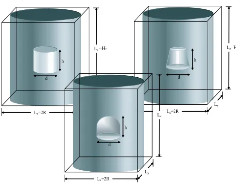
and optical properties of Sn and SnGe quantum dots. These were assumed to have cylindrical
symmetry, being either cylindrical, lens or cone shaped, with diameter (d) and height (h),
where h = d was taken for cylindrical, and h = d/2 for lens shaped (i.e. hemispherical)
dots, while h=d/2 and the base angle of 60o were taken for cone shaped dots, as shown in
Fig. 1. Although some papers report tetrakaidecahedron or truncated octahedron shapes8,
in all the observed dots.
A. The strain distribution
Due to a large difference in lattice constants of Sn (dots) and the matrix (Si, Ge) there is
a considerable strain built in the system, which strongly affects the electronic structure. The
strain was described within the continuum mechanical model and calculated by the finite
element method, as described in more detail in Ref. 12. The elastic energy of the classical
continuum medium is given by
W = 1
2
X
ijkl
Z
dV λijkl
h
eij(r)−e(0)ij (r)
i h
ekl(r)−e(0)kl (r)
i
(1)
where λijkl is the elastic tensor relating the stress and strain, eij(r) are the elastic strain
tensor components, ande(0)ij (r) the local intrinsic strain induced by the changes in the lattice constant
e(0)ij (r) =
µ
a(r)−a a
δij (2)
wherea(r) is the unstrained lattice constant at r, andais the substrate lattice constant. In crystals with the zincblende lattice (we consider only theα-Sn dots) the elastic tensor is of
the form
λijkl =C12δijδkl+C44(δikδjl+δilδjk) +Can 3
X
p=1
δipδjpδkpδlp (3)
where C12,C44 and Can =C11−C12−2C44 are the elastic constants.
In order to find the strain distribution, the finite element method is used to minimize
the total elastic energy. The continuum real space is divided into a nonuniform rectangular
grid, and the displacement components are expressed in terms of displacements at grid
points, using the first order Lagrange interpolation. The minimization was performed by
the conjugate gradient method13. The results of strain calculation for cylindrical, lens and
cone shaped Sn dots in Si are shown in Fig. 2. The calculated strain field components are
used in the eight-band k·p calculation, described in the next section.
B. The eight-band k·p model
The Γ-valley electronic structure and interband optical matrix elements of Sn quantum
conduction band Γ−7 and the valence bands Γ+8 (heavy hole and light hole bands) and Γ+7 (spin-orbit split-off band), including the strain dependent coupling and shifts of these bands.
In particular, the form given by Bahder14 was employed. The Hamiltonian is given as
H =Hk+Hs, where Hs is the strain part and Hk the kinetic part (that also includes the
modulated potentialV0(r) and the spin-orbit interactionHso).
The orthonormal wavefunction expansion method was used to find the size-quantized
states (eigenenergies and wavefunctions) in a quantum dot. Due to the cylindrical symmetry
of the dots considered here, these are taken to be embedded in an outer cylinder of radius
Rt and height Ht, with hard walls. Therefore, the envelope function corresponding to band
i was written as a linear combination of expansion basis functions
ψi(r) =
X
nl
Ainlfnm(i)(r)gl(z) Φm(φ), (4)
where
fnm(r) =
√
2
Rt
Jm(knmr)
¯
¯J|m|+1(knmRt) ¯ ¯
, (5)
gl(z) =
1
√ Ht
exp
µ i2πlz
Ht
, (6)
Φm(φ) =
1
√
2πexp (imφ), (7)
where l and m are integers and n a positive integer, and Jm is the Bessel function of order
m and knmRt is its n-th zero. Furthermore, m(i) = mf −mj(i), where mj(i) is the z
-component of angular momentum of the Bloch function |i >, and quantum number mf is
the z-component of the total angular momentum, which is a good quantum number and is
the sum of the angular momentum of the Bloch function and that of the envelope function.
The states can therefore be labeled as nemf (nhmf), denoting that an electron (hole) is in
the n-th state among the states with the z-component of the total angular momentum mf.
To find the optical absorption cross section of a transition from an initial stateito a final
state f, the interaction Hamiltonian with photons is found fromH′ =H¡
k+ e
~A
¢
−H(k), whereA=εAis the magnetic vector potential, considered constant in space, and where the quadratic terms in A were neglected, ε is the radiation polarization vector15. The optical
cross section of the i→f transition, due to electromagnetic radiation of angular frequency
ω is given by12
σε if =
2π
¯
nε0cω |
where Mif = hi|H′|fi is the matrix element which depends on the direction of light
po-larization, ¯n is refractive index, c is speed of light in vacuum, ε0 is the vacuum dielectric
constant, and Ei and Ef are the initial and final state energies, respectively. In order to
account for the spread of sizes of self-assembled quantum dots, and various other sources of
line broadening, the lineshape function g in Eq. (8) was taken as the Gaussian distribution
function, i.e.
g(Ef −Ei−~ω,2σ) =
1
σ√2πexp ·
−(Ef −Ei−~ω)
2
2σ2
¸
, (9)
where σ is the standard deviation of the Gaussian, which typically amounts to 10% of the
transition energy for bound-to-bound transitions. The selection rules for the transitions
are |∆m| = 0 for absorption of z-polarized radiation and |∆m| = 1 for in-plane-polarized
radiation.
The k·p calculation requires the parameters describing the bulk band structure of the constituent materials. In nonpolar (Si, Ge, Sn) zincblende crystals these are: Luttinger
parameters γ1,2,3, Kane energy Ep, band gap Eg, spin-orbit splitting ∆so, hydrostatic (ac
and av), uniaxial (b) and shear (d) deformation potentials, and A′ which describes the
remote band effects on the conduction band. For Si and Ge all these are well tabulated
in the literature, while the data for Sn are more scarce or completely missing. Therefore,
the Sn parameters were extracted from the empirical pseudopotential method (EPM), and
those of the values which have been reported previously could also be compared against the
values obtained here, for improved reliability, as described in the next section.
The highest valence band states in Sn dots (just as in almost all other semiconductors
except lead chalcogenides) are derived from the Γ point of the bulk Brillouin zone. If the
lowest conduction band state also turns out to be at Γ, the Sn dots would be a direct band
gap material. The main ‘competitor’ to these are the states derived from the conduction
band atLpoint, since it is much lower than theX point in Sn. The eight-bandk·pmethod cannotsimultaneouslydeliver states atL(a much more elaborate, 30-band k·pmethod16, or
e.g. the pseudopotential calculation17, would be required for that). In this work, however,
we chose to find the L-valley size-quantized states of Sn dots in an approximate manner,
using a simple effective mass calculation. For this purpose we use the scalar, angle-averaged
effective mass of the ellipsoidal L valleys, and account for the hydrostatic strain only, while
ignoring higher order effects, like the intervalley interference18 etc., which cannot be simply
as the k·p calculation at Γ, this should still suffice for comparison of direct and indirect gaps in Sn dots. The parameters required were also extracted from the EPM calculation
described below.
C. The nonlocal empirical pseudopotential method
The band structure of bulk α-Sn was modelled by the nonlocal empirical pseudopotential
method19. While requiring some experimental input, this method generally offers a better
accuracy for various band structure parameters than does the first-principles density
func-tional theory in the local density approximation without any addifunc-tional schemes like GW
approximation or “scissors correction”, as are employed in total energy approaches (see e.g.
Ref. 20 for comparison), and it is exactly these band-structure, rather than the ground-state
parameters which are of interest in the present work. The electronic structure is found by
solving the Schor¨odinger equation
Heffψn,k(r) =ǫn,kψn,k(r), (10)
in the plane wave basis
ψn,k(r) =
1
√
Ω0
eik·rX
G
an,k(G)ei G·r
, (11)
wherekis the wave vector in the first Brillouin zone,Gare the reciprocal lattice vectors and Ω0 is the volume of the primitive cell. The Hamiltonian has local, non-local, and spin-orbit
interaction parts:
Heff =Hloc+Hnon−loc+Hso. (12)
The local part is
Hloc(G′,G) = ~
2
2m(G+k)
2
δG,G′ +V(G−G′), (13)
where
V(G−G′) = X
α
Sα(G−G′)Vα(G−G′), (14)
and Vα(G−G′) andSα(G−G′) are the pseudopotential form factor and the lattice
The nonlocal potential matrix elements relating the basis states with wavevectors Kand K′ are19
VN L α (K,K
′) = 4π
Ω0
Al(E) (2l+ 1)Pl(cos (θK,K′))
×Si(K
−K′)Fi
l(K,K′), (15)
where
Fl(K,K′) =
R3 s 2 £ j2
l (KRs)−jl−1(KRs)jl+1(KRs)
¤
, K=K′
R2
s K2
−K′2
Kjl+1(KRs)jl(K′Rs)
−K′jl+1(K′Rs)jl(KRs)
, K6=K′
(16)
where K = G+k and K′ = G′+k, l is the azimuthal quantum number, cos (θK,K′) =
K·K′/|K·K′|, Pl is the Lagrange polynomial of order l , the potential strength Al is the
depth (or height) of the nonlocal square well, Rs is its radius (characterizing the particular
atomic type), jl is the spherical Bessel function of order l, and Ω0 is the volume of the unit
cell. The parameters for Sn given in Ref. 19 were used in this work.
The spin-orbit interaction Hamiltonian, in the plane wave basis, is
Hso(K′,K) =
−iλσ·(K−K′)·Si(K
−K′), (17)
where λ is the spin-orbit coupling constant, characterizing the particular atomic type, and
σ are the Pauli matrices.
For bulk bandstructure calculations one usually uses the discrete set of local
pseudopo-tential formfactors, at exactly those values ofGwhich correspond to the equilibrium lattice constant. To extract the deformation potentials, however, one has to consider lattices
de-formed by uniaxial, shear, or hydrostatic strain, which requires either a continuous local
pseudopotential form function Vα(q), or some means of interpolation. The same problem
arises in EPM based supercell calculations for superlattices, quantum dots, etc. For Si and
Ge, for instance, Friedel et al.21 have devised such formfunctions, of modified Falicov form
Vα(q) = 1 2
µ
a1(q2 −a2)
1 +e(a3(q2−a4))
¶ ·
tanh
µ
a5−q2
a6
+ 1
¸
, (18)
where q is magnitude of the wavevector, and this form, with improved parameters, has
subsequently been employed for various calculations, e.g. Refs. 22,23. We have started with
the formfactors for Sn19, and devised the corresponding formfunction for Sn that reproduces
a cutoff of 8 Ry, which gives almost full convergence, are given in Table I, along with those
for Si and Ge, Ref. 22. The nonlocal and the spin-orbit parts, on the other hand, are already
given as continuous functions of the wavevector, and need no further modification for the
present purpose.
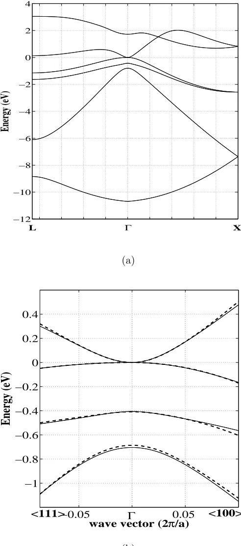
The band structure of bulk α-Sn along the L−Γ−X lines, calculated with these
pa-rameters, is given in Fig. 3. Near the Γ-point the EPM bandstructure should coincide with
that obtained by the k·p method (since it is the second order perturbation theory applied at the Γ point), with appropriately chosen material parameters, and this can be used to
extract these parameters28. Fitting of the two band structures (including the cases with
strain) was performed here by the simulated annealing algorithm13. It should be noted that
the (almost)full congruence can be obtained only in an infinitesimally small vicinity of the
Γ-point, while a very good congruence can be achieved in a finite range of kvectors around Γ, say 8–10% of the full span of the Brillouin zone (the range where the k·p method is usually considered accurate), and in this work we have targeted the latter choice. The set
of parameters for Sn, obtained that way, is given in Table II, together with those for Si and
Ge (the later two adopted from Refs. 29,30). Finally, the A′ parameter values of Si and Ge were found by using the relation for the conduction band effective mass m∗ at the Γ point
~2
2m0
(1 +A′) = ~
2
2m∗ −
P2 0
Eg+13∆
, (19)
whereP2
0 =~2EP/2m0, and the values of 0.528m0and 0.038m0for Si and Ge, respectively29.
The Luttinger γ parameters extracted here for Sn, Table II, are considerably different
from those given in Ref. 24. However, the effective masses for heavy holes which follow from
the two sets are very similar (0.2 in the [001] direction, and 0.55–0.59 in the [111] direction).
For light electrons our parameters give the effective masses of 0.018–0.019, and those from
Ref. 24 are 0.035–0.039, i.e. differing by a factor of two. However, the experimental values
for the latter (Table V in Ref. 24) are around 0.024, which is much closer to our value (not
unexpected, since we used a more empirical-related method of band structure calculation).
Therefore, we believe that the other parameters for Sn, reported here, are also reasonably
reliable. We should also note that the conduction and valence band hydrostatic deformation
potentials, ac and av, were individually determined by setting the energy at Γ+8 (heavy hole
and light hole band) for zero value of the hydrostatic strain, ǫ=ǫxx+ǫxx+ǫxx = 0, as the
constant reference energy, and then applying strain to find ac =
¡
and av =
¡
Γ+8 (ǫ)−Γ+8 (ǫ= 0)¢ /ǫ.
As for the L-valley parameters, the longitudinal (ml) and transverse (mt) effective mass
are found to be 1.99m0 and 0.091m0, respectively, in good agreement with other published
values 1.35m0, 1.48m0 and 0.072m0, 0.075m0, respectively24,31, and a value of -2.24 eV was
extracted for the hydrostatic deformation potential.
The final ingredient required for the k·p calculations of heterostructures is the valence band offset at the interface. In the absence of any more reliable experimental data, for Sn
grown on SixGeySn1−x−y we have used an expression in accordance to Jaros35, i.e. ∆Vv.b. =
1.17·x+ 0.69·y [eV]. The band energies on the absolute energy scale are not intrinsically
contained in the pseudopotential formfactors, and therefore cannot be obtained within the
EPM.
III. RESULTS AND DISCUSSION
Using the methods and materials parameters described above, we have investigated the
electronic and optical properties of the Sn-based quantum dots, in particular Sn quantum
dots embedded in Si36, and the Ge
1−xSnx alloy dots. To check the validity of the method
we have first done calculations for lens shaped Ge quantum dots in Si, with the diameter
and the height of about 100 and 15 nm, respectively. The direct interband transition onset
is about 1.3 eV, and the indirect transition (towards the L-point) onset is about 0.72 eV.
This is in good agreement with the experimental results of absorption spectrum of the
self-assembled Ge/Si quantum dots grown by a solid-source molecular beam epitaxy, in the
Stranski-Kranstanov growth mode37, where a broad peak at 0.7 to 1.0 eV was found.
A. Sn quantum dots
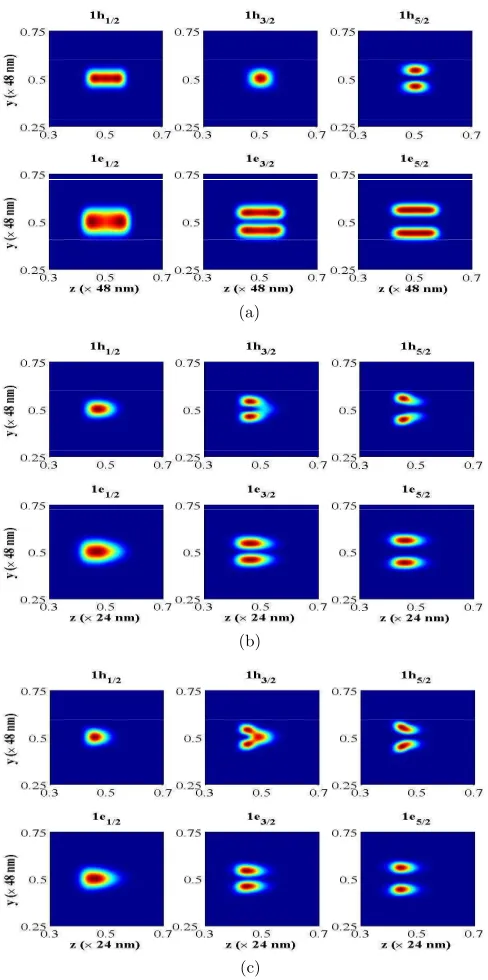
The electronic structure of Sn dots in Si was calculated assuming they were either
cylin-drical, lens or cone shaped. While the actually grown dots were approximately cylincylin-drical,
it is plausible to expect that the other two shapes might be achieved starting with a graded,
rather than uniform-composition, Sn-Si alloy layer, which is then annealed. The Sn/Si
in-terface has type-I band alignment, i.e. the Sn dot is the potential well for both electrons and
in the conduction (valence) band at Γ are given in Fig. 4. The direct-transition absorption
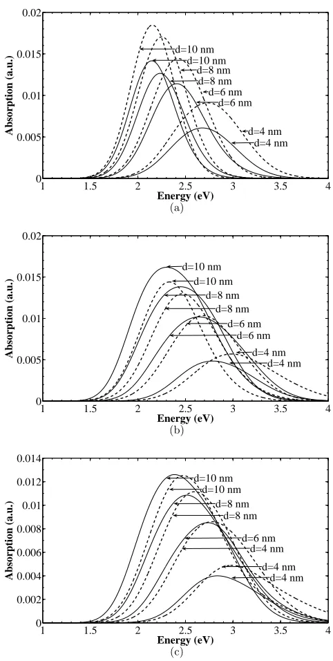
spectrum of a couple of dot sizes, for the three shapes, is shown in Fig. 5. As expected,
the transition energy inversely depends on the dot size, and also depends on the dot shape
in the expected manner, being shifted to somewhat higher energies for lens and cone dots.
Interestingly, the dot shape determines whether the z-polarized or in-plane-polarized light
would be more strongly absorbed.
The main feature from these calculations is that the direct absorption spectrum of Sn/Si
dots peaks around 2–2.5 eV. This is larger than the indirect absorption onset in bulk Si
(matrix), at about 1.1 eV, but since this absorption is relatively weak one can still expect
that these direct transitions might be observed in very thin layers of Si containing Sn dots.
It is quite a surprising result that the direct transition energies are so large. This is because
of the very large strain in Sn, so large, in fact, that is has converted a zero-gap material into
an almost wide-bandgap semiconductor.
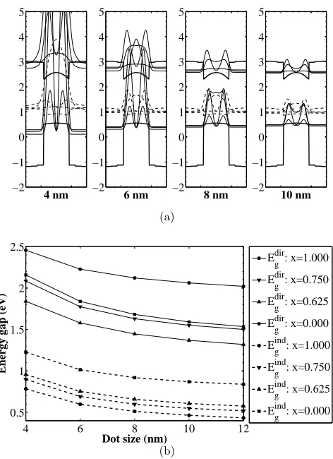
However, calculation ofL-valley quantized states (the band alignment is here also type-I)
shows that these states are much lower in energy than the conduction band states at Γ,
as shown in Fig. 6, hence the Sn/Si quantum dots are not a direct gap material. This
is a consequence of the fact that the absolute value of L-valey hydrostatic deformation
potential is much smaller than that of the Γ valley. Therefore, the effects of strain change
the arrangement of Γ and L-valley states. The photoluminescence peak at approx. 0.7 eV,
observed in Ref. 10 in Sn dots with the diameter of about 5 nm, agrees very well with the
indirect transition energy predicted here, so we believe that it is actually this (indirect and
weak) transition that was observed. The likely mechanism for this was the photogeneration
of electrons in the X valley of the Si matrix, followed by their capture into lower lying L
states of Sn dots, and then by the indirect, phonon-assisted recombination.
B. SnxGe1−x quantum dots
Previous studies of Si-Ge-Sn bulk alloys2–7show that a direct gap material can be obtained
in a suitable range of Ge1−xSnx alloy compositions, so we have also calculated the electronic
structure of Ge1−xSnx quantum dots embedded in Si. Clearly, such dots cannot be grown in
Si in the same way as Sn dots are, because Ge is completely soluable in Si, in contrast to Sn.
matrix, has been recently reported38,39. The dots are approximately hemispherical in shape,
they are covered by SiO2, and are asserted to have a coherent interface with the underlying
Si, and are therefore strained. It is less clear, however, what strain conditions apply towards
the ‘upper’ interface with SiO2, since it even has a different crystalline structure. The strain
conditions are important in Sn based dots, as shown above, but are difficult to resolve in
the case of Si/Ge1−xSnx/SiO2 dots. Furthermore, the different crystalline structures of Sn
and SiO2 would discourage one to use the k·p method at all, but the fact that the band
discontinuities between Sn and SiO2 are very large effectively makes it irrelevant what is on
the other side of Sn, and the k·p method can still be used to a good accuracy. Overall, we expect that the calculation for Ge1−xSnx quantum dots fully embedded in Si, with their axis
in the [001] direction, as was performed in this work, is an approximate description of the
actual structure.
In these calculations the Luttinger parameters, deformation potentials and the spin-orbit
splitting of Ge1−xSnx were estimated using Vegard’s law, while the direct band gap and
lat-tice constant were calculated by using the quadratic interpolation, with bowing parameters
of 2.49 eV2,4,40 and 0.166 ˚A41, respectively. The results for the dot sizes between 4 and 12
nm, and for different compositions 0≤ x≤ 1, show that the indirect interband transitions
(towards the Lvalley states) occur from 0.8 to 0.4 eV, while the direct interband transition
occur from 2.5 to 1.5 eV, as also shown in Fig. 6(b), implying that they are indirect gap
materials. The direct energy band gap depends quadratically on the Sn composition (note
the non-monotonic dependence of Eg on x in Fig. 6(b)), because the bowing parameter in
the direct band gap of the alloy has a strong influence. Experimentally, for dots of small
diameters (<10 nm) the absorption peaks between 1.5 eV and 2 eV were found38, which
agrees very well (perhaps surprisingly so, in view of the approximations involved) with the
data for direct transitions given in Fig. 6(b). Nevertheless, these dots are (predicted to be)
an indirect band gap material.
Finally, we have also made calculations for Sn dots embedded in Ge, which can be
fab-ricated in the same manner as Sn/Si dots, due to the small solubility of Sn in Ge. Here we
find the type-II alignment (after the strain), i.e. the dot is the potential well only for holes,
but not for either Γ orL-valley electrons. The conduction band edge atLis well below that
at Γ inside the Sn dot, since it is largely determined by strain, and this does not change too
matrix (which presumably could also be grown by the same technique) cannot become a
prominent direct gap material for any value of x.
IV. CONCLUSION
Using the nonlocal empirical pseudopotential method to extract the k·p parameters and deformation potentials of bulk Sn, and the 8×8 k·p method to calculate the electronic structure and optical properties of quantum dots, we have explored the properties of
self-assembled Sn dots embedded in Si, and Ge1−xSnx quantum dots in Si or in Ge, relevant for
optoelectronic applications. Cylindrical, lens and truncated cone shaped dots were
consid-ered. The self-assembled Sn/Si dots of size between 4 nm and 12 nm were found to have
indirect interband transitions (towards the L-valley size-quantized states) from 0.8 to 0.4
eV, and direct interband transitions from 2.5 to 2.0 eV. The indirect interband transition
energies compare very well with the experimental reported absorption peaks10. However,
the indirect nature of the lowest interband transition makes Sn or SnGe quantum dots in Si
matrix the unlikely candidates for optoelectronic devices, except perhaps for pure absorption
1 G. Sun, H. H. Cheng, J. Menendez, J. B. Khurgin, and R. A. Soref, Appl. Phys. Lett. 90,
11992 (1990).
2 G. He, and H. A. Atwater, Phys. Rev. Lett. 79, 1937 (1997).
3 M. Bauer, J. Taraci, J. Tolle, A. V. G. Chizmeshya, S. Zollner, D. J. Smith, J. Menendez, C.
Hu, and J. Kouvetakis, Appl. Phys. Lett. 81, 2992 (2002).
4 P. Moontragoon, Z. Ikoni´c, and P. Harrison, Semicond. Sci. Technol. 22, 742 (2007).
5 J. Kouvetakis, J. Men´endez, and A. G. V. Chizmeshya, Annual Review of Materials Research
36, 497 (2006).
6 J. Kouvetakis, and A. G. V. Chizmeshya, J. Mater. Chem. 17, 1649 (2007).
7 Y. Lei, P. Mock, T. Topuria, N. D. Browning, R. Ragan, K. S. Min, and H. A. Atwater, Appl.
Phys. Lett. 82, 4262 (2003).
8 I. Arslan, T. J. V. Yates, N. D. Browning, and P. A. Midgley, Science 309, 2195 (2005). 9 R. Ragan, K. S. Min, and H. A. Atwater, Materials Science and Engineering B 87, 204 (2001). 10 A. Karim, G.V. Hansson, W.-X. Ni, P.O. Holtz, M. Larsson and H.A. Atwater, Optical
Mate-rials 27, 836 (2005).
11 R. Ragan, Ph.D. dissertation, California Institute of Technology, 2002.
12 N. Vukmirovi´c, ˇZ. Gaˇcevi´c, Z. Ikoni´c, D. Indjin, P. Harrison, and V. Milanovi´c, Semicond. Sci.
Technol. 21, 1098 (2006).
13 W. H. Press, S. A. Teukolsky, W. T. Vetterling, and B. P. Flannery Numerical Recipes in
Fortran 77 (Cambridge University Press, Cambridge, 1992).
14 T. B. Bahder, Phys. Rev. B 41, 11992 (1990).
15 Z. Ikoni´c, V. Milanovi´c, and M. Tadi´c, J. Phys.: Condens. Matter 7, 7045 (1995). 16 S. Richard, F. Aniel, and G. Fishman, Phys. Rev. B 70, 235204 (2004).
17 L. W. Wang, A. Franceschetti, and A. Zunger, Phys. Rev. Lett. 78, 2819 (1997). 18 D. Ahn, J. Appl. Phys. 98, 033709 (2005).
19 J. R. Chelikowsky, and M. L. Cohen, Phys. Rev. B 14, 556 (1976).
20 H. Lopez, A. N. Chantis, J. Sune, and X. Cartoixa, J. Computational Electronics6, 195 (2007). 21 P. Friedel, M. S. Hybertsen, and M. Schl¨uter, Phys. Rev. B 39, 7974 (1989).
23 P. Yu, J. Wu, and B. F. Zhu, Phys. Rev. B 73, 235328 (2006).
24 T. Brudevoll, D. S. Citrin, M. Cardona, and N. E. Cristensen, Phys. Rev. B 48, 8629 (1993). 25 S. Adachi, J. Appl. Phys. 66, 813 (1989).
26 H. U. Middelmann, L. Sorba, V. Hinkel, and K. Horn, angle-resolved photoemission”, Phys.
Rev. B 35, 718 (1987).
27 G. P. Srivastava, J. Phys. C: Solid State Phys. 16, 1649 (1983).
28 D. J. Dugdale, S. Brand, and R. A. Abram, Phys. Rev. B 61, 12933 (2000).
29 S. Ridene, K. Boujdaria, H. Bouchriha, and G. Fishman, Phys. Rev. B 64, 085329 (2001). 30 C. G. Van de Walle, Phys. Rev. B 39, 1871 (1989).
31 M. Cardona, and F. H. Pollak, Phys. Rev. 142, 530 (1966). 32 P. Lawaetz, Phys. Rev. B 4, 3460 (1971).
33 B. L. Booth, and A. W. Ewald, Phys. Rev. 168, 805 (1968). 34 B. J. Roman, and A. W. Ewald, Phys. Rev. B 5, 3914 (1972). 35 M. Jaros, Phys. Rev. B 37, 7112 (1988).
36 P. Mock, Y. Lei, T. Topuria, N. D. Browning, R. Ragan, K. S. Min, and H. A. Atwater Physical
Chemistry of Interfaces and Nanomaterials 4807, 71 (2002).
37 Z. Yang, Y. Shi, J. Liu, B. Yan, R. Zhang, Y. Zheng, and K. Wang Materials Letters 58, 3765
(2004).
38 Y. Nakamura, A. Masada, and M. Ichikawa, Appl. Phys. Lett. 91, 013109 (2007).
39 Y. Nakayama, K. Takase, T. Hirahara, S. Hasegawa, T. Okuda, A. Harasawa, I. Matsuda, Y.
Nakamura, and M. Ichikawa, Japan. J. Appl. Phys. 46, L1176 (2007).
40 V. R. D’Costa, C. S. Cook, A. G. Birdwell, C. L. Littler, M. Canonico, S. Zollner, J. Kouvetakis,
and J. Men´endez, Phys. Rev. B 73, 125207 (2006).
41 P. Aella, C. Cook, J. Tolle, S. Zollner, A. V. G. Chizmeshya, and J. Kouvetakis, Appl. Phys.
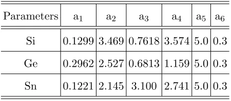
Parameters a1 a2 a3 a4 a5 a6
[image:18.595.193.418.71.170.2]Si 0.1299 3.469 0.7618 3.574 5.0 0.3 Ge 0.2962 2.527 0.6813 1.159 5.0 0.3 Sn 0.1221 2.145 3.100 2.741 5.0 0.3
TABLE I: Parameters of the pseudopotential ofα-Sn (this work), and for Si and Ge, Ref. 22. The normalization (lattice) volumes for Si, Ge, and Sn are 134.3, 151.8, and 230.5 a.u., respectively.
Value(unit)
Parameter Sn (this work) Sn (other sources) Si Ge
γ1 -25.19 -12.0
a),-14.97b),-19.2c) 4.285 13.38
γ2 -15.11 -8.45a),-10.61b),-13.2c) 0.339 4.24
γ3 -13.53 -6.84
a),-8.52b),-9.0c) 1.446 5.69
Ep 14.26 eV 23.8b) eV 21.60 eV 26.30 eV
A′ -3.25 -4.285 -7.519 ac -8.714 eV ac+av=-7.04a) 1.98 eV -8.24 eV
av 1.62 eV 2.46 eV 1.24 eV
b -2.01 eV -2.3d) -2.1 eV -2.9 eV
d -0.39 eV -4.1d) -4.8 eV -5.3 eV ∆ 0.70 eV 0.72a),0.77b) eV 0.044 eV 0.29 eV
Eg -0.408 eV -0.406a)-0.413b) eV 4.185 eV 0.898 eV
[image:18.595.141.468.364.661.2]Lx=2R
Ly
Lz
d h
Lx=2R
Ly
Lz
d h
Lx=2R
Ly
Lz
d h
[image:19.595.186.425.72.261.2]=Ht =Ht
(a)
(b)
[image:20.595.179.429.73.653.2](c)
−12 −10 −8 −6 −4 −2 0 2 4
Γ
Energy (eV)
L X
(a)
−0.05 0.05
−1 −0.8 −0.6 −0.4 −0.2 0 0.2 0.4
wave vector (2π/a)
Energy (eV)
<111> Γ <100>
(b)
[image:21.595.183.429.75.631.2](a)
(b)
[image:22.595.184.428.73.563.2](c)
1 1.5 2 2.5 3 3.5 4 0 0.005 0.01 0.015 0.02 Energy (eV)
Absorption (a.u.) d=4 nm d=4 nm d=6 nm d=6 nm d=10 nm d=10 nm d=8 nm d=8 nm (a)
1 1.5 2 2.5 3 3.5 4
0 0.005 0.01 0.015 0.02 Energy (eV) Absorption (a.u.) d=4 nm d=4 nm d=6 nm d=6 nm d=8 nm d=8 nm d=10 nm d=10 nm (b)
1 1.5 2 2.5 3 3.5 4
0 0.002 0.004 0.006 0.008 0.01 0.012 0.014 Energy (eV)
Absorption (a.u.) d=4 nm
[image:23.595.184.425.75.553.2]d=4 nm d=4 nm d=6 nm d=8 nm d=8 nm d=10 nm d=10 nm (c)
−2 −1 0 1 2 3 4 5
4 nm −2
−1 0 1 2 3 4 5
6 nm −2
−1 0 1 2 3 4 5
8 nm −2
−1 0 1 2 3 4 5 10 nm (a)
4 6 8 10 12
0.5 1 1.5 2 2.5
Dot size (nm)
Energy gap (eV)
E g dir : x=1.000 E g
dir: x=0.750
E
g
dir: x=0.625
E
g
dir: x=0.000
Egind: x=1.000
E
g
ind: x=0.750
E
g
ind: x=0.625
E
g
ind: x=0.000
(b)
[image:24.595.190.426.75.400.2]