VHDL:
Programming
by Example
Douglas L. Perry
Fourth Edition
McGraw-Hill
New York •Chicago •San Francisco •Lisbon •London Madrid •Mexico City •Milan •New Delhi •San Juan
Copyright © 2002 by The McGraw-Hill Companies, Inc. All rights reserved. Manufactured in the United States of America. Except as permitted under the United States Copyright Act of 1976, no part of this publication may be reproduced or distributed in any form or by any means, or stored in a database or retrieval system, without the prior written permission of the publisher.
0-07-140070-2
All trademarks are trademarks of their respective owners. Rather than put a trademark symbol after every occurrence of a trade-marked name, we use names in an editorial fashion only, and to the benefit of the trademark owner, with no intention of infringe-ment of the trademark. Where such designations appear in this book, they have been printed with initial caps.
McGraw-Hill eBooks are available at special quantity discounts to use as premiums and sales promotions, or for use in corporate training programs. For more information, please contact George Hoare, Special Sales, at [email protected] or (212) 904-4069.
TERMS OF USE
This is a copyrighted work and The McGraw-Hill Companies, Inc. (“McGraw-Hill”) and its licensors reserve all rights in and to the work. Use of this work is subject to these terms. Except as permitted under the Copyright Act of 1976 and the right to store and retrieve one copy of the work, you may not decompile, disassemble, reverse engineer, reproduce, modify, create derivative works based upon, transmit, distribute, disseminate, sell, publish or sublicense the work or any part of it without McGraw-Hill’s prior con-sent. You may use the work for your own noncommercial and personal use; any other use of the work is strictly prohibited. Your right to use the work may be terminated if you fail to comply with these terms.
THE WORK IS PROVIDED “AS IS”. McGRAW-HILL AND ITS LICENSORS MAKE NO GUARANTEES OR WARRANTIES AS TO THE ACCURACY, ADEQUACY OR COMPLETENESS OF OR RESULTS TO BE OBTAINED FROM USING THE WORK, INCLUDING ANY INFORMATION THAT CAN BE ACCESSED THROUGH THE WORK VIA HYPERLINK OR OTHERWISE, AND EXPRESSLY DISCLAIM ANY WARRANTY, EXPRESS OR IMPLIED, INCLUDING BUT NOT LIMITED TO IMPLIED WARRANTIES OF MERCHANTABILITY OR FITNESS FOR A PARTICULAR PURPOSE. McGraw-Hill and its licensors do not warrant or guarantee that the functions contained in the work will meet your requirements or that its operation will be uninterrupted or error free. Neither McGraw-Hill nor its licensors shall be liable to you or anyone else for any inaccuracy, error or omission, regardless of cause, in the work or for any damages resulting therefrom. McGraw-Hill has no responsibility for the con-tent of any information accessed through the work. Under no circumstances shall McGraw-Hill and/or its licensors be liable for any indirect, incidental, special, punitive, consequential or similar damages that result from the use of or inability to use the work, even if any of them has been advised of the possibility of such damages. This limitation of liability shall apply to any claim or cause what-soever whether such claim or cause arises in contract, tort or otherwise.
DOI: 10.1036/0071409548
Foreword xiii Preface xv
Acknowledgments xviii
Chapter 1 Introduction to VHDL 1
VHDL Terms 2
Describing Hardware in VHDL 3
Entity 3
Architectures 4
Concurrent Signal Assignment 5
Event Scheduling 6
Statement Concurrency 6 Structural Designs 7 Sequential Behavior 8 Process Statements 9 Process Declarative Region 9 Process Statement Part 9 Process Execution 10 Sequential Statements 10 Architecture Selection 11 Configuration Statements 11 Power of Configurations 12
Chapter 2 Behavioral Modeling 15
Introduction to Behavioral Modeling 16 Transport Versus Inertial Delay 20
Inertial Delay 20
Transport Delay 21
Inertial Delay Model 22 Transport Delay Model 23 Simulation Deltas 23
Drivers 27
Driver Creation 27
Bad Multiple Driver Model 28
Generics 29
Block Statements 31
Chapter 3 Sequential Processing 39
Process Statement 40
Sensitivity List 40
Process Example 40
Signal Assignment Versus Variable Assignment 42
Incorrect Mux Example 43
Correct Mux Example 45
Sequential Statements 46
IF Statements 47
CASE Statements 48
LOOP Statements 50
NEXT Statement 53
EXIT Statement 54
ASSERT Statement 56
Assertion BNF 57
WAIT Statements 59
WAIT ON Signal 62
WAIT UNTIL Expression 62
WAIT FOR time_expression 62
Multiple WAIT Conditions 63
WAIT Time-Out 64
Sensitivity List Versus WAIT Statement 66
Concurrent Assignment Problem 67
Passive Processes 70
Chapter 4 Data Types 73
Object Types 74
Signal 74
Variables 76
Constants 77
Data Types 78
Scalar Types 79
Composite Types 86
Incomplete Types 98
File Types 102
File Type Caveats 105
Subtypes 105
Chapter 5 Subprograms and Packages 109
Subprograms 110
Conversion Functions 113
Resolution Functions 119
Procedures 133
Packages 135
Package Declaration 136
Deferred Constants 136
Subprogram Declaration 137
Package Body 138
Chapter 6 Predefined Attributes 143
Value Kind Attributes 144
Value Type Attributes 144
Value Array Attributes 147
Value Block Attributes 149
Function Kind Attributes 151
Function Type Attributes 151
Function Array Attributes 154
Function Signal Attributes 156
Attributes ’EVENT and ’LAST_VALUE 157
Attribute ’LAST_EVENT 158
Attribute ’ACTIVE and ’LAST_ACTIVE 160
Signal Kind Attributes 160
Attribute ’DELAYED 161
Attribute ’STABLE 164
Attribute ’QUIET 166
Attribute ’TRANSACTION 168
Type Kind Attributes 169
Range Kind Attributes 170
Chapter 7 Configurations 173
Default Configurations 174
Component Configurations 176
Lower-Level Configurations 179
Entity-Architecture Pair Configuration 180
Port Maps 181
Mapping Library Entities 183
Generics in Configurations 185
Generic Value Specification in Architecture 188 Generic Specifications in Configurations 190
Board-Socket-Chip Analogy 195
Block Configurations 199
Chapter 8 Advanced Topics 205
Overloading 206
Subprogram Overloading 206
Overloading Operators 210
Aliases 215
Qualified Expressions 215
User-Defined Attributes 218
Generate Statements 220
Irregular Generate Statement 222
TextIO 224
Chapter 9 Synthesis 231
Register Transfer Level Description 232
Constraints 237
Timing Constraints 238
Clock Constraints 238
Attributes 239
Load 240
Drive 240
Arrival Time 240
Technology Libraries 241
Synthesis 243
Translation 243
Boolean Optimization 244
Flattening 245
Factoring 246
Mapping to Gates 247
Chapter 10 VHDL Synthesis 251
Simple Gate — Concurrent Assignment 252
IF Control Flow Statements 253
Case Control Flow Statements 256
Simple Sequential Statements 257
Asynchronous Reset 259
Asynchronous Preset and Clear 261
More Complex Sequential Statements 262
Four-Bit Shifter 264
Chapter 11 High Level Design Flow 273
RTL Simulation 275
VHDL Synthesis 277
Functional Gate-Level Verification 283
Place and Route 284
Post Layout Timing Simulation 286
Static Timing 287
Chapter 12 Top-Level System Design 289
CPU Design 290
Top-Level System Operation 290
Instructions 291
Sample Instruction Representation 292
CPU Top-Level Design 293
Block Copy Operation 299
Chapter 13 CPU: Synthesis Description 303
ALU 306
Comp 309
Control 311
Reg 321
Regarray 322
Shift 324
Trireg 326
Chapter 14 CPU: RTL Simulation 329
Testbenches 330
Kinds of Testbenches 331
Stimulus Only 333
Full Testbench 337
Simulator Specific 340
Hybrid Testbenches 342
Fast Testbench 345
CPU Simulation 349
Chapter 16 Place and Route 369
Place and Route Process 370
Placing and Routing the Device 373
Setting up a project 373
Chapter 17 CPU: VITAL Simulation 379
VITAL Library 381
VITAL Simulation Process Overview 382
VITAL Implementation 382
Simple VITAL Model 383
VITAL Architecture 386
Wire Delay Section 386
Flip-Flop Example 388
SDF File 392
VITAL Simulation 394
Back-Annotated Simulation 397
Chapter 18 At Speed Debugging Techniques 399
Instrumentor 401
Debugger 401
Debug CPU Design 401
Create Project 402
Specify Top-Level Parameters 403
Specify Project Parameters 403
Instrument Signals 404
Write Instrumented Design 405
Implement New Design 405
Start Debug 406
Enable Breakpoint 406
Trigger Position 408
Waveform Display 408
Set Watchpoint 409
Complex Triggers 410
Appendix A Standard Logic Package 413
Appendix B VHDL Reference Tables 435
Appendix D VHDL93 Updates 449
Alias 449
Attribute Changes 450
Bit String Literal 452
DELAY_LENGTH Subtype 452
Direct Instantiation 452
Extended Identifiers 453
File Operations 454
Foreign Interface 455
Generate Statement Changes 456
Globally Static Assignment 456
Groups 457
Incremental Binding 458
Postponed Process 459
Pure and Impure Functions 460
Pulse Reject 460
Report Statement 461
Shared Variables 461
Shift Operators 463
SLL — shift left logical 463
SRL — shift right logical 463
SLA — shift left arithmetic 463
SRA — shift right arithmetic 463
ROL — rotate left 464
ROR — rotate right 464
Syntax Consistency 464
Unaffected 466
XNOR Operator 466
Index 469
VHDL has been at the heart of electronic design productivity since ini-tial ratification by the IEEE in 1987. For almost 15 years the electronic design automation industry has expanded the use of VHDL from initial concept of design documentation, to design implementation and func-tional verification. It can be said that VHDL fueled modern synthesis technology and enabled the development of ASIC semiconductor compa-nies. The editions of Doug Perry’s books have served as the authoritative source of practical information on the use of VHDL for users of the language around the world.
The use of VHDL has evolved and its importance increased as semi-conductor devices dimensions have shrunk. Not more than 10 years ago it was common to mix designs described with schematics and VHDL. But as design complexity grew, the industry abandoned schematics in favor of the hardware description language only. The successive revisions of this book have always kept pace with the industry’s evolving use of VHDL.
The fact that VHDL is adaptable is a tribute to its architecture. The industry has seen the use of VHDL’s package structure to allow design-ers, electronic design automation companies and the semiconductor indus-try to experiment with new language concepts to ensure good design tool and data interoperability. When the associated data types found in the IEEE 1164 standard were ratified, it meant that design data interoper-ability was possible.
All of this was facilitated by industry backing in a consortium of systems, electronic design automation and semiconductor companies now known as Accellera.
And when the ASIC industry needed a standard way to convey gate-level design data and timing information in VHDL, one of Accellera’s progenitors (VHDL International) sponsored the IEEE VHDL team to build a companion standard. The IEEE 1076.4 VITAL (VHDL Initiative Towards ASIC Libraries) was created and ratified as offers designers a single language flow from concept to gate-level signoff.
methodologies and the external connections provided to the hardware description languages.
But from the beginning, the leadership of the VHDL community has assured open and internationally accredited standards for the electronic design engineering community. The legacy of this team’s work continues to benefit the design community today as the benchmark by which one measures openness.
The design community continues to see benefits as the electronic design automation community continues to find new algorithms to work from VHDL design descriptions and related standards to again push designer productivity. And, as a new generation of designers of programmable logic devices move to the use of hardware description languages as the basis of their design methodology, there will be substantial growth in the number of VHDL users.
This new generation of electronic designers, along with the current designers of complex systems and ASICs, will find this book as invalu-able as the first generation of VHDL users did with the first addition. Updated with current use of the standard, all will benefit from the years of use that have made the VHDL language the underpinning of successful electronic design.
This is the fourth version of the book and this version now not only provides VHDL language coverage but design methodology information as well. This version will guide the reader through the process of creating a VHDL design, simulating the design, synthesizing the design, placing and routing the design, using VITAL simulation to verify the final result, and a new technique called At-Speed debugging that provides extremely fast design verification. The design example in this version has been updated to reflect the new focus on the design methodology.
This book was written to help hardware design engineers learn how to write good VHDL design descriptions. The goal is to provide enough VHDL and design methodology information to enable a designer to quickly write good VHDL designs and be able to verify the results. It will also attempt to bring the designer with little or no knowledge of VHDL, to the level of writing complex VHDL descriptions. It is not intended to show every pos-sible construct of VHDL in every pospos-sible use, but rather to show the de-signer how to write concise, efficient, and correct VHDL descriptions of hardware designs.
This book is organized into three logical sections. The first section of the book will introduce the VHDL language, the second section walks through a VHDL based design process including simulation, synthesis, place and route, and VITAL simulation; and the third section walks through a design example of a small CPU design from VHDL capture to final gate-level implementation, and At-Speed debugging. At the back of the book are included a number of appendices that contain useful information about the language and examples used throughout the book.
range of types available for use in VHDL. Examples are given for each of the types showing how they would be used in a real example. In Chapter 5 the concepts of subprograms and packages are introduced. The different uses for functions are given, as well as the features available in VHDL packages.
Chapter 6 introduces the five kinds of VHDL attributes. Each attribute kind has examples describing how to use the specific attribute to the designer’s best advantage. Examples are given which describe the pur-pose of each of the attributes.
Chapters 7 and 8 will introduce some of the more advanced VHDL features to the reader. Chapter 7 discusses how VHDL configurations can be used to construct and manage complex VHDL designs. Each of the different configuration styles are discussed along with examples showing usage. Chapter 8 introduces more of the VHDL advanced top-ics with discussions of overloading, user defined attributes, generate statements, and TextIO.
The second section of the book consists of Chapters 9 through 11. Chap-ters 9 and 10 discuss the synthesis process and how to write synthesiz-able designs. These two chapters describe the basics of the synthesis process including how to write synthesizeable VHDL, what is a technol-ogy library, what does the synthesis process look like, what are con-straints and attributes, and what does the the optimization process look like. Chapter 11 discusses the complete high level design flow from VHDL capture through VITAL simulation.
The third section of the book walks through a description of a small CPU design from the VHDL capture through simulation, synthesis, place and route, and VITAL simulation. Chapter 12 describes the top level of the CPU design from a functional point of view. In Chapter 13 the RTL description of the CPU is presented and discussed from a synthesis point of view. Chapter 14 begins with a discussion of VHDL testbenches and how they are used to verify functionality. Chapter 14 finishes the discus-sion by describing the simulation of the CPU design. In Chapter 15 the verified design is synthesized to a target technology. Chapter 16 takes the synthesized design and places and routes the design to a target device. Chapter 17 begins with a discussion of VITAL and ends with the VITAL simulation of the placed and routed CPU design. Chapter 18 is a new chapter that discusses the new technique of At-Speed debugging. This chapter provides the reader with an in-depth look at how a hardware implementation of the CPU design can help speed verification.
1
Introduction to
VHDL
The VHSIC Hardware Description Language is an industry standard language used to describe hardware from the abstract to the concrete level. VHDL resulted from work done in the ’70s and early ’80s by the U.S. Department of Defense. Its roots are in the ADA language, as will be seen by the overall structure of VHDL as well as other VHDL statements.
VHDL usage has risen rapidly since its inception and is used by literally tens of thousands of engineers around the globe to create sophisticated electronic products. This chapter will start the process of easing the reader into the complexities of VHDL. VHDL is a powerful language with numerous language constructs that are capable of describing very complex behavior. Learning all the features of VHDL is not a simple task. Complex features will be introduced in a simple form and then more complex usage will be described.
In 1986, VHDL was proposed as an IEEE standard. It went through a number of revisions and changes until it was adopted as the IEEE 1076 standard in December 1987. The IEEE 1076-1987 standard VHDL is the VHDL used in this book. (Appendix D contains a brief description of VHDL 1076-1993.) All the examples have been described in IEEE 1076 VHDL, and compiled and simulated with the VHDL simulation environment from Model Technology Inc. The synthesis examples were synthesized with the Exemplar Logic Inc. synthesis tools.
VHDL Terms
Before we go any further, let’s define some of the terms that we use throughout the book. These are the basic VHDL building blocks that are used in almost every description, along with some terms that are redefined in VHDL to mean something different to the average designer.
■ Entity. All designs are expressed in terms of entities. An entity is the most basic building block in a design. The uppermost level of the design is the top-level entity. If the design is hierarchical, then the top-level description will have lower-level descriptions contained in it. These lower-level descriptions will be lower-level entities contained in the top-level entity description.
■ Architecture. All entities that can be simulated have an architec-ture description. The architecarchitec-ture describes the behavior of the entity. A single entity can have multiple architectures. One archi-tecture might be behavioral while another might be a structural description of the design.
■ Configuration. A configuration statement is used to bind a component instance to an entity-architecture pair. A configuration can be considered like a parts list for a design. It describes which behavior to use for each entity, much like a parts list describes which part to use for each part in the design.
■ Package. A package is a collection of commonly used data types and subprograms used in a design. Think of a package as a tool-box that contains tools used to build designs.
■ Bus. The term “bus” usually brings to mind a group of signals or a particular method of communication used in the design of hard-ware. In VHDL, a bus is a special kind of signal that may have its drivers turned off.
■ Attribute. An attribute is data that are attached to VHDL objects or predefined data about VHDL objects. Examples are the current drive capability of a buffer or the maximum operating temperature of the device.
■ Generic. A generic is VHDL’s term for a parameter that passes information to an entity. For instance, if an entity is a gate level model with a rise and a fall delay, values for the rise and fall delays could be passed into the entity with generics.
■ Process. A process is the basic unit of execution in VHDL. All operations that are performed in a simulation of a VHDL descrip-tion are broken into single or multiple processes.
Describing Hardware in VHDL
VHDL Descriptions consist of primary design units and secondary design units. The primary design units are the Entity and the Package. The sec-ondary design units are the Architecture and the Package Body. Sec-ondary design units are always related to a primary design unit. Libraries are collections of primary and secondary design units. A typical design usually contains one or more libraries of design units.
Entity
A VHDL entity specifies the name of the entity, the ports of the entity, and entity-related information. All designs are created using one or more entities.
Let’s take a look at a simple entity example:
ENTITY mux IS
The keyword ENTITYsignifies that this is the start of an entity state-ment. In the descriptions shown throughout the book, keywords of the language and types provided with the STANDARD package are shown in ALL CAPITAL letters. For instance, in the preceding example, the key-words are ENTITY, IS, PORT, IN, INOUT, and so on. The standard type pro-vided is BIT. Names of user-created objects such as mux, in the example above, will be shown in lower case.
The name of the entity is mux. The entity has seven ports in the PORT clause. Six ports are of mode INand one port is of mode OUT. The four data input ports (a, b, c, d) are of type BIT. The two multiplexer select inputs, s0and s1, are also of type BIT. The output port is of type BIT.
The entity describes the interface to the outside world. It specifies the number of ports, the direction of the ports, and the type of the ports. A lot more information can be put into the entity than is shown here, but this gives us a foundation upon which we can build more complex examples.
Architectures
The entity describes the interface to the VHDL model. The architec-ture describes the underlying functionality of the entity and contains the statements that model the behavior of the entity. An architecture is always related to an entity and describes the behavior of that entity. An architecture for the counter device described earlier would look like this:
ARCHITECTURE dataflow OF mux IS SIGNAL select : INTEGER; BEGIN
select <= 0 WHEN s0 = ‘0’ AND s1 = ‘0’ ELSE 1 WHEN s0 = ‘1’ AND s1 = ‘0’ ELSE 2 WHEN s0 = ‘0’ AND s1 = ‘1’ ELSE 3;
x <= a AFTER 0.5 NS WHEN select = 0 ELSE b AFTER 0.5 NS WHEN select = 1 ELSE c AFTER 0.5 NS WHEN select = 2 ELSE d AFTER 0.5 NS;
END dataflow;
The reason for the connection between the architecture and the entity is that an entity can have multiple architectures describing the behavior of the entity. For instance, one architecture could be a behavioral description, and another could be a structural description.
The textual area between the keyword ARCHITECTUREand the keyword BEGIN is where local signals and components are declared for later use. In this example signal select is declared to be a local signal.
The statement area of the architecture starts with the keyword BEGIN. All statements between the BEGINand the ENDnetlist statement are called concurrent statements, because all the statements execute concurrently.
Concurrent Signal Assignment
In a typical programming language such as C or C++, each assignment statement executes one after the other and in a specified order. The order of execution is determined by the order of the statements in the source file. Inside a VHDL architecture, there is no specified ordering of the assignment statements. The order of execution is solely specified by events occurring on signals that the assignment statements are sensitive to.
Examine the first assignment statement from architecture behave, as shown here:
select <= 0 WHEN s0 = ‘0’ AND s1 = ‘0’ ELSE 1 WHEN s0 = ‘1’ AND s1 = ‘0’ ELSE 2 WHEN s0 = ‘0’ AND s1 = ‘1’ ELSE 3;
A signal assignment is identified by the symbol <=. Signal selectwill get a numeric value assigned to it based on the values of s0and s1. This statement is executed whenever either signal s0or signal s1has an event occur on it. An event on a signal is a change in the value of that signal. A signal assignment statement is said to be sensitive to changes on any sig-nals that are to the right of the <= symbol. This signal assignment state-ment is sensitive to s0and s1. The other signal assignment statement in architecture dataflowis sensitive to signal select.
statement will not execute because this statement is not sensitive to changes to signal a. This happens because signal a is not on the right side of the operator. The second signal assignment statement will exe-cute because it is sensitive to events on signal a. When the second signal assignment statement executes the new value of a will be assigned to signal x. Output port xwill now change to 1.
Let’s now look at the case where signal s0changes value. Assume that s0and s1 are both 0, and ports a, b, c, and dhave the values 0, 1, 0, and 1, respectively. Now let’s change the value of port s0from 0 to 1. The first signal assignment statement is sensitive to signal s0and will there-fore execute. When concurrent statements execute, the expression value calculation will use the current values for all signals contained in it.
When the first statement executes, it computes the new value to be as-signed to q from the current value of the signal expression on the right side of the <=symbol. The expression value calculation uses the current values for all signals contained in it.
With the value of s0equal to 1 and s1 equal to 0, signal selectwill receive a new value of 1. This new value of signal selectwill cause an event to occur on signal select, causing the second signal assignment statement to execute. This statement will use the new value of signal select to assign the value of port b to port x. The new assignment will cause port xto change from a 0 to a 1.
Event Scheduling
The assignment to signal x does not happen instantly. Each of the values assigned to signal xcontain an AFTER clause. The mechanism for delaying the new value is called scheduling an event. By assigning port xa new value, an event was scheduled 0.5 nanoseconds in the future that contains the new value for signal x.When the event matures (0.5 nanoseconds in the future), signal xreceives the new value.
Statement Concurrency
The two signal assignment statements in architecture behaveform a behavioral model, or architecture, for the muxentity. The dataflow archi-tecture contains no structure. There are no components instantiated in the architecture. There is no further hierarchy, and this architecture can be considered a leaf node in the hierarchy of the design.
Structural Designs
Another way to write the muxdesign is to instantiate subcomponents that perform smaller operations of the complete model. With a model as simple as the 4-input multiplexer that we have been using, a simple gate level description can be generated to show how components are described and instantiated. The architecture shown below is a structural description of the muxentity.
ARCHITECTURE netlist OF mux IS COMPONENT andgate
PORT(a, b, c : IN bit; c : OUT BIT); END COMPONENT;
COMPONENT inverter
PORT(in1 : IN BIT; x : OUT BIT); END COMPONENT;
COMPONENT orgate
PORT(a, b, c, d : IN bit; x : OUT BIT); END COMPONENT;
SIGNAL s0_inv, s1_inv, x1, x2, x3, x4 : BIT;
BEGIN
U1 : inverter(s0, s0_inv); U2 : inverter(s1, s1_inv);
U3 : andgate(a, s0_inv, s1_inv, x1); U4 : andgate(b, s0, s1_inv, x2); U5 : andgate(c, s0_inv, s1, x3); U6 : andgate(d, s0, s1, x4);
U7 : orgate(x2 => b, x1 => a, x4 => d, x3 => c, x => x); END netlist;
This description uses a number of lower-level components to model the behavior of the muxdevice. There is an inverter component, an andgate component and an orgatecomponent. Each of these components is declared in the architecture declaration section, which is between the architecture statement and the BEGINkeyword.
The architecture statement area is located after the BEGINkeyword. In this example are a number of component instantiation statements. These statements are labeled U1-U7. Statement U1is a component instantiation statement that instantiates the inverter component. This statement con-nects port s0 to the first port of the inverter component and signal
s0_invto the second port of the inverter component. The effect is that port in1of the inverter is connected to port s0of the muxentity, and port
xof the inverter is connected to local signal s0_inv. In this statement the ports are connected by the order they appear in the statement.
Notice component instantiation statement U7. This statement uses the following notation:
U7 : orgate(x2 => b, x1 => a, x4 => d, x3 => c, x => x);
This statement uses named association to match the ports and signals to each other. For instance port x2of the orgateis connected to port bof the entity with the first association clause. The last instantiation clause connects port xof the orgatecomponent to port xof the entity. The order of the clauses is not important. Named and ordered association can be mixed, but it is not recommended.
Sequential Behavior
There is yet another way to describe the functionality of a mux device in VHDL. The fact that VHDL has so many possible representations for sim-ilar functionality is what makes learning the entire language a big task. The third way to describe the functionality of the muxis to use a process statement to describe the functionality in an algorithmic representation. This is shown in architecture sequential, as shown in the following:
ARCHITECTURE sequential OF mux IS (a, b, c, d, s0, s1 )
VARIABLE sel : INTEGER; BEGIN
IF s0 = ‘0’ and s1 = ‘0’ THEN sel := 0;
ELSIF s0 = ‘1’ and s1 = ‘0’ THEN sel := 1;
ELSIF s0 = ‘0’ and s1 = ‘0’ THEN sel := 2;
ELSE
WHEN 0 => x <= a; WHEN 1 => x <= b; WHEN 2 => x <= c; WHEN OTHERS =>
x <= d; END CASE; END PROCESS; END sequential;
The architecture contains only one statement, called a process state-ment. It starts at the line beginning with the keyword PROCESSand ends with the line that contains END PROCESS. All the statements between these two lines are considered part of the process statement.
Process Statements
The process statement consists of a number of parts. The first part is called the sensitivity list; the second part is called the process declarative part; and the third is the statement part. In the preceding example, the list of signals in parentheses after the keyword PROCESSis called the sen-sitivity list. This list enumerates exactly which signals cause the process statement to be executed. In this example, the list consists of a, b, c, d, s0, and s1. Only events on these signals cause the process statement to be executed.
Process Declarative Region
The process declarative part consists of the area between the end of the sensitivity list and the keyword BEGIN. In this example, the declarative part contains a variable declaration that declares local variable sel. This variable is used locally to contain the value computed based on ports s0 and s1.
Process Statement Part
sequential statements. This means that any statements enclosed by the process are executed one after the other in a sequential order just like a typical programming language. Remember that the order of the statements in the architecture did not make any difference; however, this is not true inside the process. The order of execution is the order of the statements in the process statement.
Process Execution
Let’s see how this works by walking through the execution of the example in architecture sequential, line by line. To be consistent, let’s assume that s0changes to 0. Because s0is in the sensitivity list for the process statement, the process is invoked. Each statement in the process is then executed sequentially. In this example the IFstatement is executed first followed by the CASEstatment. Each check that the IFstatement performs is done sequentially starting with the first in the model.
The first check is to see if s0is equal to a 0. This statement fails because s0is equal to a 1 and s1t is equal to a 0. The signal assignment state-ment that follows the first check will not be executed. Instead, the next check is performed. This check succeeds and the signal assignment state-ments following the check for s0 = 1 and s1 = 0 are executed. This statement is shown below.
sel := 1;
Sequential Statements
This statement will execute sequentially. Once it is executed, the next check of the IFstatement is not performed. Whenever a check succeeds, no other checks are done. The IFstatement has completed and now the CASE statement will execute. The CASEstatement will evaluate the value of sel computed earlier by the IF statement and then execute the appropriate statement that matches the value of sel. In this example the value of sel is 1 therefore the following statement will be executed:
x <= b;
Architecture Selection
So far, three architectures have been described for one entity. Which archi-tecture should be used to model the muxdevice? It depends on the accuracy wanted and if structural information is required. If the model is going to be used to drive a layout tool, then the structural architecture netlist is probably most appropriate. If a structural model is not wanted for some other reason, then a more efficient model can be used. Either of the other two methods (architectures dataflowand sequential) are probably more efficient in memory space required and speed of execution. How to choose between these two methods may come down to a question of programming style. Would the modeler rather write concurrent or sequential VHDL code? If the modeler wants to write concurrent VHDL code, then the style of architecture dataflowis the way to go; otherwise, architecture sequential should be chosen. Typically, modelers are more familiar with sequen-tial coding styles, but concurrent statements are very powerful tools for writing small efficient models.
We will also look at yet another architecture that can be written for an entity. This is the architecture that can be used to drive a synthesis tool. Synthesis tools convert a Register Transfer Level(RTL) VHDL description into an optimized gate-level description. Synthesis tools can offer greatly enhanced productivity compared to manual methods. The synthesis process is discussed in Chapters 9, “Synthesis” and 10, “VHDL Synthesis.”
Configuration Statements
An entity can have more than one architecture, but how does the modeler choose which architecture to use in a given simulation? The configuration statement maps component instantiations to entities. With this powerful statement, the modeler can pick and choose which architectures are used to model an entity at every level in the design.
Let’s look at a configuration statement using the netlist architecture of the rsffentity. The following is an example configuration:
CONFIGURATION muxcon1 OF mux IS FOR netlist
FOR U1,U2 :
inverter USE ENTITY WORK.myinv(version1); END FOR;
FOR U3,U4,U5,U6 : andgate USE ENTITY WORK.myand(ver-sion1);
FOR U7 : orgate USE ENTITY WORK.myor(version1); END FOR;
END FOR; END muxcon1;
The function of the configuration statement is to spell out exactly which architecture to use for every component instance in the model. This occurs in a hierarchical fashion. The highest-level entity in the design needs to have the architecture to use specified, as well as any components instantiated in the design.
The preceding configuration statement reads as follows: This is a con-figuration named muxcon1for entity mux. Use architecture netlistas the architecture for the topmost entity, which is mux. For the two component instances U1 and U2 of type inverterinstantiated in the netlist archi-tecture, use entity myinv, architecture version1from the library called WORK. For the component instances U3-U6 of type andgate, use entity myand, architecture version1from library WORK. For component instance U7 of type orgate use entity myor, architecture version1 from library WORK. All of the entities now have architectures specified for them. Entity muxhas architecture netlist, and the other components have architectures named version1specified.
Power of Configurations
By compiling the entities, architectures, and the configuration specified earlier, you can create a simulatable model. But what if you did not want to simulate at the gate level? What if you really wanted to use architecture BEHAVEinstead? The power of the configuration is that you do not need to recompile your complete design; you only need to recompile the new config-uration. Following is an example configuration:
CONFIGURATION muxcon2 OF mux IS FOR dataflow
END FOR; END muxcon2;
This is a configuration named muxcon2for entity mux. Use architecture dataflow for the topmost entity, which is mux. By compiling this configuration, the architecture dataflowis selected for entity muxin this simulation.
SUMMARY
In this chapter, we have had a basic introduction to VHDL and how it can be used to model the behavior of devices and designs. The first example showed how a simple dataflow model in VDHL is specified. The second example showed how a larger design can be made of smaller designs —in this case a 4-input multiplexer was modeled using AND, ORand IN-VERTERgates. The first example provided a structural view of VHDL.
2
Behavioral
Modeling
In Chapter 1, we discussed different modeling techniques and touched briefly on behavioral modeling. In this chapter, we discuss behavioral modeling more thoroughly, as well as some of the issues relating to the simulation and syn-thesis of VHDL models.
Introduction to Behavioral
Modeling
The signal assignment statement is the most basic form of behavioral modeling in VHDL. Following is an example:
a <= b;
This statement is read as follows: agets the value of b. The effect of this statement is that the current value of signal bis assigned to signal a. This statement is executed whenever signal bchanges value. Signal b is in the sensitivity list of this statement. Whenever a signal in the sen-sitivity list of a signal assignment statement changes value, the signal assignment statement is executed. If the result of the execution is a new value that is different from the current value of the signal, then an event is scheduled for the target signal. If the result of the execution is the same value, then no event is scheduled but a transaction is still generated (transactions are discussed in Chapter 3, “Sequential Processing”). A trans-action is always generated when a model is evaluated, but only signal value changes cause events to be scheduled.
The next example shows how to introduce a nonzero delay value for the assignment:
a <= b after 10 ns;
This statement is read as follows: a gets the value of b when 10 nanoseconds of time have elapsed.
Both of the preceding statements are concurrent signal assignment state-ments. Both statements are sensitive to changes in the value of signal b. Whenever bchanges value, these statements execute and new values are assigned to signal a.
Using a concurrent signal assignment statement, a simple AND gate can be modeled, as follows:
ENTITY and2 IS
PORT ( a, b : IN BIT; PORT ( c : OUT BIT ); END and2;
ARCHITECTURE and2_behav OF and2 IS BEGIN
A
B
C
Figure 2-1
AND Gate Symbol.
END and2_behav;
The AND gate has two inputs a, band one output c, as shown in Figure 2-1. The value of signal cmay be assigned a new value whenever either aor bchanges value. With an AND gate, if ais a ‘0’and bchanges from a ‘1’to a ‘0’, output cdoes not change. If the output does change value, then a transaction occurs which causes an event to be scheduled on signal c; otherwise, a transaction occurs on signal c.
The entity design unit describes the ports of the and2gate. There are two inputs aand b, as well as one output c. The architecture and2_behav for entity and2contains one concurrent signal assignment statement. This statement is sensitive to both signal aand signal b by the fact that the expression to calculate the value of cincludes both aand bsignal values. The value of the expression aand bis calculated first, and the resulting value from the calculation is scheduled on output c, 5 nanoseconds from the time the calculation is completed.
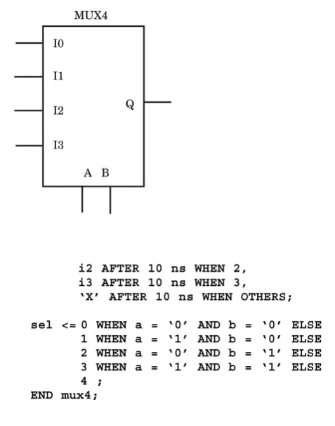
The next example shows more complicated signal assignment state-ments and demonstrates the concept of concurrency in greater detail. In Figure 2-2, the symbol for a four-input multiplexer is shown.
This is the behavioral model for the mux:
LIBRARY IEEE;
USE IEEE.std_logic_1164.ALL;
ENTITY mux4 IS
PORT ( i0, i1, i2, i3, a, b : IN std_logic; PORT ( i0, i1, i2, i3, a, q : OUT std_logic); END mux4;
ARCHITECTURE mux4 OF mux4 IS SIGNAL sel: INTEGER;
BEGIN
WITH sel SELECT
I0 I1
A B Q MUX4
[image:37.531.132.371.70.373.2]I3 I2
Figure 2-2
Mux4 Symbol.
q <= i2 AFTER 10 ns WHEN 2, q <= i3 AFTER 10 ns WHEN 3, q <= ‘X’ AFTER 10 ns WHEN OTHERS;
sel <= 0 WHEN a = ‘0’ AND b = ‘0’ ELSE 1 WHEN a = ‘1’ AND b = ‘0’ ELSE 2 WHEN a = ‘0’ AND b = ‘1’ ELSE 3 WHEN a = ‘1’ AND b = ‘1’ ELSE 4 ;
END mux4;
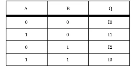
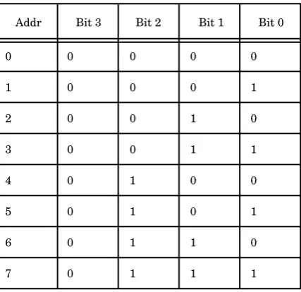
The entity for this model has six input ports and one output port. Four of the input ports (I0, I1, I2, I3) represent signals that will be assigned to the output signal q. Only one of the signals will be assigned to the out-put signal qbased on the value of the other two input signals aand b. The truth table for the multiplexer is shown in Figure 2-3.
To implement the functionality described in the preceding, we use a conditional signal assignment statement and a selected signal assignment. The second statement type in this example is called a conditional signal assignment statement. This statement assigns a value to the target sig-nal based on conditions that are evaluated for each statement. The statement WHENconditions are executed one at a time in sequential order until the conditions of a statement are met. The first statement that matches the conditions required assigns the value to the target signal. The target signal for this example is the local signal sel. Depending on the values of signals a and b, the values 0 through 4 are assigned to sel.
A B Q
0 0 I0
1 0 I1
0 1 I2
[image:38.531.141.370.75.191.2]1 1 I3
Figure 2-3
Mux Functional Table.
matches does the assign, and the other matching statements’ values are ignored.
The first statement is called a selected signal assignment and selects among a number of options to assign the correct value to the target sig-nal. The target signal in this example is the signal q.
The expression (the value of signal selin this example) is evaluated, and the statement that matches the value of the expression assigns the value to the target signal. All of the possible values of the expression must have a matching choice in the selected signal assignment (or an OTHERS clause must exist).
Each of the input signals can be assigned to output q, depending on the values of the two select inputs, aand b. If the values of aor bare unknown values, then the last value, ‘X’ (unknown), is assigned to output q. In this example, when one of the select inputs is at an unknown value, the out-put is set to unknown.
Looking at the model for the multiplexer, it looks like the model will not work as written. It seems that the value of signal selis used before it is computed. This impression is received from the fact that the second statement in the architecture is the statement that actually computes the value for sel. The model does work as written, however, because of the concept of concurrency.
The second statement is sensitive to signals aand b. Whenever either aor bchanges value, the second statement is executed, and signal selis updated. The first statement is sensitive to signal sel. Whenever signal selchanges value, the first signal assignment is executed.
based on the sophistication of the synthesis tool and the constraints put on the design.
Transport Versus Inertial Delay
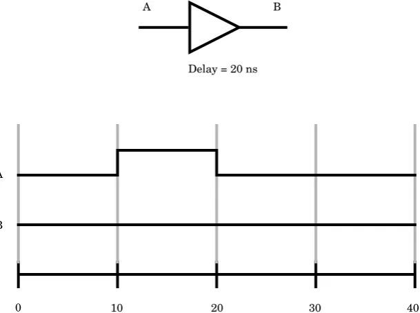
In VHDL, there are two types of delay that can be used for modeling behaviors. Inertial delay is the most commonly used, while transport delay is used where a wire delay model is required.
Inertial Delay
Inertial delay is the default in VHDL. If no delay type is specified, iner-tial delay is used. Ineriner-tial delay is the default because, in most cases, it behaves similarly to the actual device.
In an inertial delay model, the output signal of the device has inertia, which must be overcome for the signal to change value. The inertia value is equal to the delay through the device. If there are any spikes, pulses, and so on that have periods where a signal value is maintained for less than the delay through the device, the output signal value does not change. If a signal value is maintained at a particular value for longer than the delay through the device, the inertia is overcome and the device changes to the new state.
Figure 2-4 is an example of a very simple buffer symbol. The buffer has a single input A and a single output B. The waveforms are shown for input A and the output B. Signal A changes from a ‘0’to a ‘1’at 10 nanoseconds and from a ‘1’to a ‘0’at 20 nanoseconds. This creates a pulse or spike that is 10 nanoseconds in duration. The buffer has a 20- nanosecond delay through the device.
A
B
0 10 20 30 40
A B
[image:40.531.155.460.76.303.2]Delay = 20 ns
Figure 2-4
Inertial Delay Buffer Waveforms.
event at 30 nanoseconds did not have enough time to overcome the inertia of the output signal.
The inertial delay model is by far the most commonly used in all cur-rently available simulators. This is partly because, in most cases, the inertial delay model is accurate enough for the designer’s needs. One more reason for the widespread use of inertial delay is that it prevents prolific propagation of spikes throughout the circuit. In most cases, this is the behavior wanted by the designer.
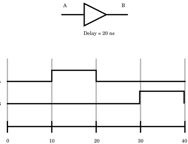
Transport Delay
Transport delay is not the default in VHDL and must be specified. It repre-sents a wire delay in which any pulse, no matter how small, is propagated to the output signal delayed by the delay value specified. Transport delay is especially useful for modeling delay line devices, wire delays on a PC board, and path delays on an ASIC.
A B
Delay = 20 ns
A
B
[image:41.531.146.451.72.305.2]0 10 20 30 40
Figure 2-5
Transport Delay Buffer Waveforms.
propagation.
At time 10 nanoseconds, the buffer model is executed and schedules an event for the output to go to a 1 value at 30 nanoseconds. At time 20 nanoseconds, the buffer model is re-invoked and predicts a new value for the output at time 40 nanoseconds. With the transport delay algorithm, the events are put in order. The event for time 40 nanoseconds is put in the list of events after the event for time 30 nanoseconds. The spike is not swallowed but is propagated intact after the delay time of the device.
Inertial Delay Model
The following model shows how to write an inertial delay model. It is the same as any other model we have been looking at. The default delay type is inertial; therefore, it is not necessary to specify the delay type to be inertial:
LIBRARY IEEE;
USE IEEE.std_logic_1164.ALL; ENTITY buf IS
ARCHITECTURE buf OF buf IS BEGIN
b <= a AFTER 20 ns; END buf;
Transport Delay Model
Following is an example of a transport delay model. It is similar in every respect to the inertial delay model except for the keyword TRANSPORTin the signal assignment statement to signal b. When this keyword exists, the delay type used in the statement is the transport delay mechanism:
LIBRARY IEEE;
USE IEEE.std_logic_1164.ALL; ENTITY delay_line IS
PORT ( a : IN std_logic; PORT ( b : OUT std_logic); END delay_line;
ARCHITECTURE delay_line OF delay_line IS BEGIN
b <= TRANSPORT a AFTER 20 ns; END delay_line;
Simulation Deltas
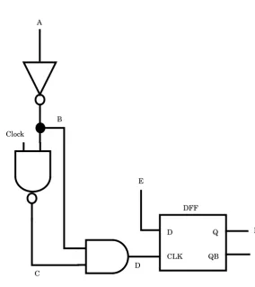
Simulation deltas are used to order some types of events during a simu-lation. Specifically, zero delay events must be ordered to produce con-sistent results. If zero delay events are not properly ordered, results can be disparate between different simulation runs. An example of this is shown using the circuit shown in Figure 2-6. This circuit could be part of a clocking scheme in a complex device being modeled. It probably would not be the entire circuit, but only a part of the circuit used to generate the clock to the D flip-flop.
The circuit consists of an inverter, a NAND gate, and an AND gate driving the clock input of a flip-flop component. The NAND gate and AND gate are used to gate the clock input to the flip-flop.
D CLK
Q
QB
DFF
A
Clock
C
D
B
E
[image:43.531.135.420.56.376.2]F
Figure 2-6
Simulation Delta Circuit.
To use delta delay, all of the circuit components must have zero delay specified. The delay for all three gates is specified as zero. (Real circuits do not exhibit such characteristics, but sometimes modeling is easier if all of the delay is concentrated at the outputs.) Let’s examine the non-delta delay mechanism first.
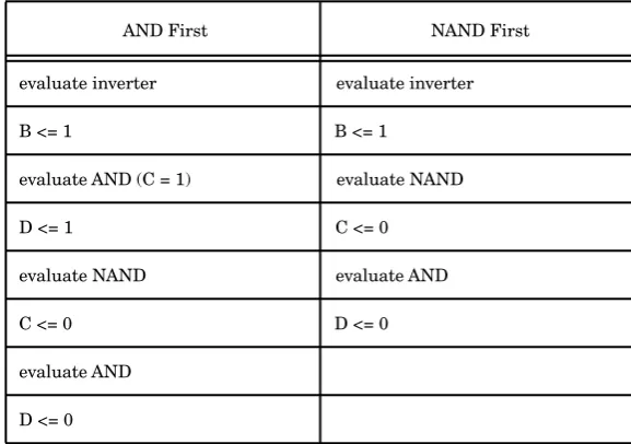
When a falling edge occurs on signal A, the output of the inverter changes in 0 time. Let’s assume that such an event occurs at time 10 nanoseconds. The output of the inverter, signal B, changes to reflect the new input value. When signal B changes, both the AND gate and the NAND gate are reevaluated. For this example, the clock input is assumed to be a constant value ‘1’. If the NAND gate is evaluated first, its new value is ‘0’.
AND First NAND First
evaluate inverter evaluate inverter
B <= 1 B <= 1
evaluate AND (C = 1) evaluate NAND
D <= 1 C <= 0
evaluate NAND evaluate AND
C <= 0 D <= 0
evaluate AND
[image:44.531.149.438.76.279.2]D <= 0
Figure 2-7
Comparison of Two Evaluation Mecha-nisms.
The NAND gate reevaluates and calculates its new value as ‘0’. The change on the output of the NAND gate causes the AND gate to reevaluate again. The AND gate now sees the value of B, a ‘1’value, and the new value of signal C, a ‘0’value. The AND gate now predicts a ‘0’on its output. This process is summarized in Figure 2-7.
Both circuits arrive at the same value for signal D. However, when the AND gate is evaluated first, a rising edge, one delta delay wide, occurs on signal D. This rising edge can clock the flip-flop, depending on how the flip-flop is modeled.
The point of this discussion is that without a delta synchronization mechanism, the results of the simulation can depend on how the simulator data structures are built. For instance, compiling the circuit the first time might make the AND gate evaluate first, while compiling again might make the NAND gate evaluate first—clearly not desirable results; simu-lation deltas prevent this behavior from occurring.
The same circuit evaluated using the VHDL delta delay mechanism would evaluate as shown in Figure 2-8.
The evaluation of the circuit does not depend on the order of evalua-tion of the NAND gate or AND gate. The sequence in Figure 2-8 occurs irrespective of the evaluation order of the AND or NAND gate.
Time Delta Activity
10 ns (1) A <= 0
evaluate inverter
(2) B <= 1 evaluate AND evaluate NAND
(3) D <= 1 C <= 0 evaluate AND
(4) D <= 0
11 ns
Figure 2-8
Delta Delay Evalua-tion Mechanism.
The inverter calculates the new value for signal B, which is the value ‘1’. This value is not propagated immediately, but is scheduled for the next delta time point (delta 2).
The simulator then begins execution of delta time point 2. Signal B is updated to a ‘1’value, and the AND gate and NAND gate are reevaluated. Both the AND gate and NAND gate now schedule their new values for the next delta time point (delta 3).
When delta 3 occurs, signal D receives a ‘1’value, and signal C receives a ‘0’value. Because signal C also drives the AND gate, the AND gate is reevaluated and schedules its new output for delta time point 4.
To summarize, simulation deltas are an infinitesimal amount of time used as a synchronization mechanism when 0 delay events are present. Delta delay is used whenever 0 delay is specified, as shown in the fol-lowing:
a <= b AFTER 0 ns;
Another case for using delta delay is when no delay is specified. For example:
a <= b;
In both cases, whenever signal bchanges value from an event, signal ahas a delta-delayed signal assignment to it.
ENTITY reg IS
PORT( a, clock : in bit PORT( d : out bit); END reg;
ARCHITECTURE test OF reg IS SIGNAL b, c : bit;
BEGIN
b <= NOT(a); -- notice no delay c <= NOT( clock AND b);
d <= c AND b; END test;
Drivers
VHDL has a unique way of handling multiply driven signals. Multiply driven signals are very useful for modeling a data bus, a bidirectional bus, and so on. Correctly modeling these kinds of circuits in VHDL requires the concept of signal drivers. A VHDL driver is one contributor to the overall value of a signal.
A multiply driven signal has many drivers. The values of all of the drivers are resolved together to create a single value for the signal. The method of resolving all of the contributors into a single value is through a resolution function(resolution functions are discussed in Chapter 5, “Subprograms and Packages”). A resolution function is a designer-written function that is called whenever a driver of a signal changes value.
Driver Creation
Drivers are created by signal assignment statements. A concurrent signal assignment inside of an architecture produces one driver for each sig-nal assignment. Therefore, multiple sigsig-nal assignments produce multiple drivers for a signal. Consider the following architecture:
ARCHITECTURE test OF test IS BEGIN
a <= b AFTER 10 ns; a <= c AFTER 10 ns; END test;
signal assignment statement creates a driver for signal a. The first state-ment creates a driver that contains the value of signal bdelayed by 10 nanoseconds. The second statement creates a driver that contains the value of signal cdelayed by 10 nanoseconds. How these two drivers are resolved is left to the designer. The designers of VHDL did not want to arbitrarily add language constraints to signal behavior. Synthesizing the preceding example would short cand btogether.
Bad Multiple Driver Model
Let’s look at a model that looks correct at first glance, but does not function as the user intended. The model is for the 4 to 1 multiplexer discussed earlier:
USE WORK.std_logic_1164.ALL; ENTITY mux IS
PORT (i0, i1, i2, i3, a, b: IN std_logic; PORT (q : OUT std_logic);
END mux;
ARCHITECTURE bad OF mux IS BEGIN
q <= i0 WHEN a = ‘0’ AND b = ‘0’ ELSE ‘0’; q <= i1 WHEN a = ‘1’ AND b = ‘0’ ELSE ‘0’; q <= i2 WHEN a = ‘0’ AND b = ‘1’ ELSE ‘0’; q <= i3 WHEN a = ‘1’ AND b = ‘1’ ELSE ‘0’; END BAD;
This model assigns i0to qwhen ais equal to a 0 and bis equal to a 0; i1when ais equal to a 1 and bis equal to a 0; and so on. At first glance, the model looks like it works. However, each assignment to signal qcreates a new driver for signal q. Four drivers to signal qare created by this model. Each driver drives either the value of one of the i0, i1, i2, i3inputs or ‘0’. The value driven is dependent on inputs aand b. If ais equal to ‘0’and bis equal to ‘0’, the first assignment statement puts the value of i0into one of the drivers of q. The other three assignment statements do not have their conditions met and, therefore, are driving the value ‘0’. Three drivers are driving the value ‘0’, and one driver is driving the value of i0. Typical resolution functions would have a difficult time predicting the desired output on q, which is the value of i0.
ARCHITECTURE better OF mux IS BEGIN
q <= i0 WHEN a = ‘0’ AND b = ‘0’ ELSE i1 WHEN a = ‘1’ AND b = ‘0’ ELSE i2 WHEN a = ‘0’ AND b = ‘1’ ELSE i3 WHEN a = ‘1’ AND b = ‘1’ ELSE ‘X’; --- unknown
END better;
Generics
Generics are a general mechanism used to pass information to an instance of an entity. The information passed to the entity can be of most types allowed in VHDL. (Types are covered in detail later in Chapter 4, “Data Types.”)
Why would a designer want to pass information to an entity? The most obvious, and probably most used, information passed to an entity is delay times for rising and falling delays of the device being modeled. Generics can also be used to pass any user-defined data types, including information such as load capacitance, resistance, and so on. For synthesis parameters such as datapath widths, signal widths, and so on, can be passed in as generics.
All of the data passed to an entity is instance-specific information. The data values pertain to the instance being passed the data. In this way, the designer can pass different values to different instances in the design.
The data passed to an instance is static data. After the model has been elaborated (linked into the simulator), the data does not change during simulation. Generics cannot be assigned information as part of a simula-tion run. The informasimula-tion contained in generics passed into a component instance or a block can be used to alter the simulation results, but results cannot modify the generics.
The following is an example of an entity for an AND gate that has three generics associated with it:
ENTITY and2 IS
GENERIC(rise, fall : TIME; load : INTEGER); PORT( a, b : IN BIT;
PORT( c : OUT BIT); END AND2;
delays, as well as the loading that the device has on its output. With this information, the model can correctly model the AND gate in the design. Following is the architecture for the AND gate:
ARCHITECTURE load_dependent OF and2 IS SIGNAL internal : BIT;
BEGIN
internal <= a AND b;
c <= internal AFTER (rise + (load * 2 ns)) WHEN internal = ‘1’ ELSE internal AFTER (fall + (load * 3 ns));
END load_dependent;
The architecture declares a local signal called internalto store the value of the expression aand b. Pre-computing values used in multiple instances is a very efficient method for modeling.
The generics rise, fall, and load contain the values that were passed in by the component instantiation statement. Let’s look at a piece of a model that instantiates the components of type AND2 in an-other model:
LIBRARY IEEE;
USE IEEE.std_logic_1164.ALL; ENTITY test IS
GENERIC(rise, fall : TIME; load : INTEGER); PORT ( ina, inb, inc, ind : IN std_logic; PORT ( out1, out2 : OUT std_logic); END test;
ARCHITECTURE test_arch OF test IS COMPONENT AND2
GENERIC(rise, fall : TIME; load : INTEGER); PORT ( a, b : IN std_logic;
PORT ( c : OUT std_logic); END COMPONENT;
BEGIN
U1: AND2 GENERIC MAP(10 ns, 12 ns, 3 ) PORT MAP (ina, inb, out1 );
U2: AND2 GENERIC MAP(9 ns, 11 ns, 5 ) PORT MAP (inc, ind, out2 );
END test_arch;
to out1. In the same way, component U2is mapped to signals inc, ind, and out2.
Generic rise of instance U1 is mapped to 10 nanoseconds, generic fallis mapped to 12 nanoseconds, and generic loadis mapped to 3. The generics for component U2 are mapped to values 9 and 11 nanoseconds and value 5.
Generics can also have default values that are overridden if actual values are mapped to the generics. The next example shows two instances of component type AND2.
In instance U1, actual values are mapped to the generics, and these values are used in the simulation. In instance U2, no values are mapped to the instance, and the default values are used to control the behavior of the simulation if specified; otherwise an error occurs:
LIBRARY IEEE;
USE IEEE.std_logic_1164.ALL; ENTITY test IS
GENERIC(rise, fall : TIME; GENERIC(load : INTEGER);
PORT ( ina, inb, inc, ind : IN std_logic; PORT ( out1, out2 : OUT std_logic);
END test;
ARCHITECTURE test_arch OF test IS COMPONENT and2
GENERIC(rise, fall : TIME := 10 NS; GENERIC(load : INTEGER := 0); PORT ( a, b : IN std_logic; PORT ( c : OUT std_logic); END COMPONENT;
BEGIN
U1: and2 GENERIC MAP(10 ns, 12 ns, 3 ) PORT MAP (ina, inb, out1 );
U2: and2 PORT MAP (inc, ind, out2 );
END test_arch;
As we have seen, generics have many uses. The uses of generics are limited only by the creativity of the model writer.
Block Statements
to logically group areas of the model. The analogy with a typical Schematic Entry system is a schematic sheet. In a typical Schematic Entry system, a level or a portion of the design can be represented by a number of schematic sheets. The reason for partitioning the design may relate to C design standards about how many components are allowed on a sheet, or it may be a logical grouping that the designer finds more understandable. The same analogy holds true for block statements. The statement area in an architecture can be broken into a number of separate logical areas. For instance, if you are designing a CPU, one block might be an ALU, another a register bank, and another a shifter.
Each block represents a self-contained area of the model. Each block can declare local signals, types, constants, and so on. Any object that can be declared in the architecture declaration section can be declared in the block declaration section. Following is an example:
LIBRARY IEEE;
USE IEEE.std_logic_1164.ALL; PACKAGE bit32 IS
TYPE tw32 IS ARRAY(31 DOWNTO 0) OF std_logic; END bit32;
LIBRARY IEEE;
USE IEEE.std_logic_1164.ALL; USE WORK.bit32.ALL;
ENTITY cpu IS
PORT( clk, interrupt : IN std_logic;
PORT( addr : OUT tw32; data : INOUT tw32 ); END cpu;
ARCHITECTURE cpu_blk OF cpu IS SIGNAL ibus, dbus : tw32; BEGIN
ALU : BLOCK
SIGNAL qbus : tw32; BEGIN
-- alu behavior statements END BLOCK ALU;
REG8 : BLOCK
SIGNAL zbus : tw32; BEGIN
REG1: BLOCK
SIGNAL qbus : tw32; BEGIN
-- reg1 behavioral statements END BLOCK REG1;