Theses Thesis/Dissertation Collections
2010
Implementation of multi-CLB designs using
quantum-dot cellular automata
Chia-Ching Tung
Follow this and additional works at:http://scholarworks.rit.edu/theses
This Thesis is brought to you for free and open access by the Thesis/Dissertation Collections at RIT Scholar Works. It has been accepted for inclusion
in Theses by an authorized administrator of RIT Scholar Works. For more information, please [email protected].
Recommended Citation
Using Quantum-dot Cellular Automata
by
Chia-Ching Tung
A Thesis Submitted in Partial Fulfillment of the Requirements for the Degree of Master of Science
in Electrical Engineering
Supervised by
Assistant Professor Dr. Eric Peskin
Department of Electrical and Microelectronic Engineering Kate Gleason College of Engineering
Rochester Institute of Technology Rochester, New York
February 2010
Approved by:
Dr. Eric Peskin, Assistant Professor
Thesis Advisor, Department of Electrical and Microelectronic Engineering
Dr. Dorin Patru, Assistant Professor
Committee Member, Department of Electrical and Microelectronic Engineering
Dr. Dhireesha Kudithipudi, Assistant Professor
Rochester Institute of Technology Kate Gleason College of Engineering
Title:
Implementation of Multi-CLB Designs Using QCA
I, Chia-Ching Tung, hereby grant permission to the Wallace Memorial Library to reproduce my thesis in whole or part.
Chia-Ching Tung
Acknowledgments
Abstract
Implementation of Multi-CLB Designs Using Quantum-dot Cellular Automata
Chia-Ching Tung
Supervising Professor: Dr. Eric Peskin
CMOS scaling is currently facing a technological barrier. Novel tech-nologies are being proposed to keep up with the need for computation power
and speed. One of the proposed ideas is thequantum-dot cellular automata
(QCA) technology. QCA uses quantum mechanical effects in the device at the molecular scale. QCA systems have the potential for low power, high density, and regularity.
This thesis studies QCA devices and uses those devices to build a
sim-ple field programmable gate array(FPGA). The FPGA is a combination of
multipleconfigure logical blocks(CLBs) tiled together. Most previous work
on this area has focused on fixed logic and programmable interconnect. In contrast, the work at the Rochester Institute of Technology (RIT) has
de-signed and simulated a configurable logic block (CLB) based on look-up
tables (LUTs). This thesis presents a simple FPGA that consists of
Contents
Acknowledgments . . . iii
Abstract . . . iv
1 Introduction. . . 1
1.1 Motivation . . . 1
1.2 Previous Work . . . 4
1.3 Contributions . . . 7
1.3.1 Proposed Design . . . 7
1.3.2 Applications . . . 8
1.4 Organization . . . 8
2 QCA Background . . . 9
2.1 Basic QCA Operation . . . 9
2.1.1 QCA Cell . . . 10
2.1.2 QCA Wire . . . 10
2.1.3 Wire Crossing . . . 11
2.1.4 Majority Gate and Inverter Gate . . . 12
2.1.5 QCA Clock . . . 14
2.1.6 Design Rules . . . 15
2.2 QCADesigner . . . 17
2.2.1 Limitations . . . 18
2.3 QCA Implementation . . . 18
2.3.2 Molecular QCA . . . 20
2.3.3 Magnetic QCA . . . 21
2.4 QCA Concept Relative to the Thesis . . . 22
3 Architectures . . . 24
3.1 FPGA . . . 24
3.2 CLB . . . 25
3.3 LUT . . . 26
3.3.1 Unit Memory . . . 28
3.3.2 Output Circuitry . . . 30
3.4 Configuration . . . 32
4 Simulation and Analysis . . . 38
4.1 Full Adder . . . 39
4.2 Ripple Carry Adder . . . 41
4.3 Bit-Serial Multiplier . . . 44
4.4 Glitchless Reconfiguration . . . 45
5 Conclusions and Future Work . . . 50
Bibliography . . . 52
A Full Adder Waveform Simulation . . . 59
B RCA Waveform Simulation . . . 67
C BSM Waveform Simulation . . . 75
List of Tables
2.1 Truth table for majority gate. . . 13
3.1 Full adder truth table. . . 36
3.2 si memory configuration. . . 36
3.3 ci+1 memory configuration. . . 36
3.4 Input for configuration. . . 37
4.1 Full adder result. . . 40
4.2 RCA result. . . 44
4.3 Glitchless reconfiguration. . . 48
4.4 Full adder result during partial reconfiguration. . . 49
B.1 RCA test vectors applied. . . 68
List of Figures
1.1 Fixed logic FPGA. . . 3
1.2 FPGA with programmable logic. . . 4
1.3 FPGA with programmable logic and programmable inter-connect. . . 5
2.1 Binary interpretation of the states of a QCA cell. . . 10
2.2 QCA normal wire. . . 11
2.3 QCA inversion chain. . . 11
2.4 Wire crossing. . . 12
2.5 QCA majority gate. . . 13
2.6 QCA inverter. . . 14
2.7 Clock zones and phases. . . 15
2.8 Normal wire connects to inversion chain. . . 16
2.9 Inversion chain tapping off. . . 16
2.10 QCA wire crossing between normal and inversion. . . 17
2.11 Metal dot QCA cell: (a) SEM image, and (b) schematic dia-gram. Reproduced from [28] with permission of the publisher. 19 2.12 Two views of a molecule as a QCA cell. Reproduced from [19] with permission of the publisher. . . 20
2.13 Different states of a molecular QCA cell: (a) +1 state, (b) non-ideal state, and (c) -1 state. Reproduced from [19] with permission of the publisher. . . 21
3.1 Architecture for QCA FPGA. . . 25
3.2 Block diagram of CLB. . . 26
3.3 CLB layout in QCADesigner [41]. . . 27
3.4 LUT. . . 29
3.5 Decoder. . . 30
3.6 Unit memory cell. . . 31
3.7 Output circuitry. . . 33
3.8 A single CLB. . . 34
3.9 Position of each address within the LUT of the CLB. . . 35
4.1 Full adder symbol. . . 39
4.2 FA simulation in QCADesigner. . . 40
4.3 Simulation result of full adder in HDLQ. . . 41
4.4 RCA block diagram. . . 41
4.5 Partial 4-bit RCA waveform result form HDLQ. . . 43
4.6 BSM block diagram. . . 46
4.7 Simulation result of glitchless reconfiguration. . . 49
A.1 Full adder waveform in QCADesigner 1 of 6. . . 60
A.2 Full adder waveform in QCADesigner 2 of 6. . . 61
A.3 Full adder waveform in QCADesigner 3 of 6. . . 62
A.4 Full adder waveform in QCADesigner 4 of 6. . . 63
A.5 Full adder waveform in QCADesigner 5 of 6. . . 64
A.6 Full adder waveform in QCADesigner 6 of 6. . . 65
A.7 Full adder waveform in HDLQ 1 of 3. . . 66
A.8 Full adder waveform in HDLQ 2 of 3. . . 66
A.9 Full adder waveform in HDLQ 3 of 3. . . 66
B.1 RCA waveform in HDLQ 1 of 12. . . 68
B.3 RCA waveform in HDLQ 3 of 12. . . 69
B.4 RCA waveform in HDLQ 4 of 12. . . 70
B.5 RCA waveform in HDLQ 5 of 12. . . 70
B.6 RCA waveform in HDLQ 6 of 12. . . 71
B.7 RCA waveform in HDLQ 7 of 12. . . 71
B.8 RCA waveform in HDLQ 8 of 12. . . 72
B.9 RCA waveform in HDLQ 9 of 12. . . 72
B.10 RCA waveform in HDLQ 10 of 12. . . 73
B.11 RCA waveform in HDLQ 11 of 12. . . 73
B.12 RCA waveform in HDLQ 12 of 12. . . 74
C.1 BSM waveform in HDLQ 1 of 5. . . 76
C.2 BSM waveform in HDLQ 2 of 5. . . 76
C.3 BSM waveform in HDLQ 3 of 5. . . 76
C.4 BSM waveform in HDLQ 4 of 5. . . 76
C.5 BSM waveform in HDLQ 5 of 5. . . 76
D.1 Glitchless reconfiguration waveform 1 of 7. . . 78
D.2 Glitchless reconfiguration waveform 2 of 7. . . 79
D.3 Glitchless reconfiguration waveform 3 of 7. . . 80
D.4 Glitchless reconfiguration waveform 4 of 7. . . 81
D.5 Glitchless reconfiguration waveform 5 of 7. . . 82
D.6 Glitchless reconfiguration waveform 6 of 7. . . 83
Chapter 1
Introduction
As of 2009, the transistor density or the number of transistors on an
inte-grated circuit (IC) chip is approaching a limit. The semiconductor industry
is still able to fabricate devices exponentially smaller according to Moore’s law [25], but as transistor sizes are shrinking to the nanometer scale, it be-comes extremely difficult to continue packing more and more computational power into our microprocessors. In the near future, the operation of transis-tors will be dominated by the physics of the quantum world. Conventional
complementary metal-oxide-semiconductor (CMOS) transistor is facing its
physical limitations [8, 9] related to power dissipation, interconnects, and fabrication. Research on a novel technology to replace the current technol-ogy is necessary. The new method has to take advantage of quantum effects and nanoscale physics in order to keep up with the ever growing need for computation power and speed.
1.1
Motivation
Currently, CMOS is the mainstream technology for fabricating chips. As more transistors are being put into the processors, the issues related to dop-ing regions, oxide thickness, diffusion barriers, power dissipation, and
leak-age current etc. become difficult to scale. All these issues call into question
the feasibility of CMOS in the future.
There is much ongoing research to find a way to replace the standard
CMOS technology. Quantum-dot cellular automata (QCA) [18], carbon
nanotube transistors (CNT) [3], silicon nanowires [12], etc. are all
(ITRS) [1] describes the difficulty that the current semiconductor technol-ogy will face. The biggest concern that the CMOS is facing is the difficulty on setting more and more devices on the chips. Approximately at 25 nm technology the fabrication process might fail to achieve this goal [8]. Quan-tum mechanical effects have an important role in device performance and induce uncertainty. QCA is an emerging nanotechnology that provides a revolutionary approach to substitute for the traditional CMOS technology
for very-large-scale integration (VLSI) fabrication. QCA technology
ad-dresses the inevitable nanoscale level issues, such as interaction between devices and operation of devices. The interaction between devices at the nanoscale level is a roadblock on further scaling of the CMOS devices. QCA also has the following potential advantages: low power consumption, higher device density, and implementation on the nanoscale level.
The current ongoing research in the field of QCA has two directions. One direction is to find a method for stable fabrication of QCA devices. In order to compete with CMOS technology, the device must have low cost, be able to operate at room temperature, and be able to handle high clock frequencies. Some significant examples of such research are [4, 10, 21, 23,
24]. Three types of QCA fabrication process have been proposed,metal-dot
QCA [21], molecular QCA [23], and magnetic QCA [5]. However, there
has not been a successful attempt to create a testable circuit of molecular QCA, and only small circuits have been fabricated by metal-dot QCA, and magnetic QCA.
The other direction of research is on the nanoarchitecture level [34],
which is the primary focus of this thesis. This area of research has focuses
on using QCA technology for circuit implementation. Taskin et al. suggest
that the general nanoarchitecture design is able to be studied by modeling QCA dots at a higher level of abstraction [34]. The high-level design is in-dependent of the manufacturing technology. Unlike power dissipation, area of the device, and operating clock frequency, the architecture level does not require hardware manufactured devices to perform experimental testing.
Field programmable gate arrays (FPGAs) [6] are reconfigurable logic
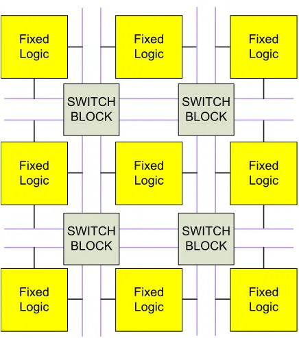
Figure 1.1: Fixed logic FPGA.
both. The logic blocks have the ability to compute complex functions of given inputs. The outputs of the logic blocks are connected and wired to-gether. FPGAs have a regular pattern in design, which may facilitate self-assembly when fabricated in nanotechnology. FPGAs can emulate many applications. If an FPGA can be built using QCA technology, it would al-low many applications to run on QCA. Therefore, creating an FPGA using QCA technology is an interesting application of QCA.
FPGAs mainly consist of an array of multiplexers,look-up tables(LUTs),
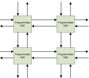
memory cells, and special hardware blocks. As mentioned in the previous paragraph, FPGAs depend on programmable logic, programmable intercon-nect, or both [7, 46]. FPGAs with fixed logic consist of a sea of fixed logic elements interconnected by a mesh of wires. The programmability is made at the point of intersection of the wires. Figure 1.1 shows a general exam-ple of fixed-logic-type FPGA. The switch blocks decide the signal routings based on the users’ configurations. Figure 1.2 shows an FPGA with pro-grammable logic. The inputs and the outputs on each side of the block are
Programmable logic
Programmable logic
Programmable logic
[image:15.612.159.462.84.348.2]Programmable logic
Figure 1.2: FPGA with programmable logic.
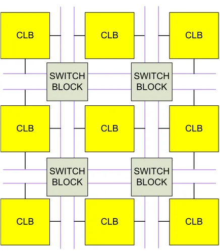
block (CLB) with fixed connections to the neighboring CLBs. Most
com-mercial FPGAs consist of both types of circuits. The configurable logic blocks are linked by programmable interconnect. Programmable intercon-nects are switching blocks that can be programmed to give various connec-tions between the logic blocks for different funcconnec-tions. Such an arrangement is shown in Figure 1.3. The black lines in Figure 1.3 represent the intercon-nections between the CLB and the switch blocks.
This thesis focuses on the programmable-logic method. This method achieves the goal through the use of LUTs. The LUT consists of a 16-bit memory and two 2-to-4 decoders. It is capable of serial write and parallel read operations with low read latency.
1.2
Previous Work
Previous work on QCA-based FPGAs has focused on programmable
Figure 1.3: FPGA with programmable logic and programmable interconnect.
based on programmable interconnect. In [27], authors develop an intercon-nect design with flexible routing. The interconintercon-nects between each block are operated by QCA cells. If the connection is to be established, the clock sig-nal is applied to the interconnect to make the QCA cells operate. When the clock is not given to the QCA cells, the connection is not established, and the cells act as open circuits. The logic block in [26,27] consists of a NAND gate. The size of logic blocks for data processing are equal to the size of the interconnect blocks. This allows the shape of the FPGA to be more compact and organized. These articles discuss the use of programmable interconnect with fixed logic, which is the FPGA architecture represented in Figure 1.1.
Amiriet al.[2] created a tree of multiplexers to be the fixed logic cell for
the FPGA. The fixed logic presented has six inputs and one output. Two of the six inputs are the control signals that decide which inputs will be routed to the output. The module can emulate any two-input or three-input logic function such as NAND, AND, OR, and NOR. The authors believe their proposed circuit could operate at terahertz frequencies. Similar to [27], the directions of all input signals are controlled by one or two control signals.
programmable interconnect in the FPGA. The PSM allows the logic blocks of the FPGA to be interconnected when needed. The PSM acts as a con-troller in the system to decide the direction and the destination of all the signals.
In contrast to the above articles, Lantz and Peskin [16] explored the method of building FPGA by programmable logic. A novel CLB design for FPGAs implementation in QCA has been presented. The CLB is built
by using four look-up tables (LUTs), each of them corresponding to one of
the four directions: north, south, east, and west. Each LUT is equipped with a decoder and 16-bit memory blocks. Each LUT is capable of taking four inputs and producing one output. The complete CLB is formed by joining four LUTs together. The CLB has separate inputs for data and for LUT reconfiguration that may be used independently. Therefore, it is possible to reconfigure the memory of the LUT while data is being processed. This CLB has four inputs and four outputs that can also combine with other CLBs or stand alone to perform digital functions. A disadvantage of the design is its high latency. The read operation requires 30 clock cycles. An FPGA is made up of an array of CLB blocks. Each CLB is capable of implement-ing an independent function. The output of the CLBs can be combined to implement a complex function of the input variables. The signals will tra-verse multiple CLBs. Therefore, the latency will accumulate and become an important issue. Optimizing to reduce the latency and area of the design is necessary.
CMOS memories to avoid unused area. The FPGA studied in this thesis will be an array of multiple copies of the CLB presented by [32, 36].
1.3
Contributions
In contrast to [2, 15, 26, 27, 39]. This thesis presents an FPGA based on
configurable logic. In contrast to [16, 32], this thesis creates a small FPGA
consisting ofmultipleCLBs.
1.3.1 Proposed Design
This thesis presents the design and simulation of a CLB-based FPGA us-ing QCA technology, and applications along with the FPGA. The FPGA in
the thesis is considered to be the composition of configurable logic blocks
(CLBs). The FPGA architecture presented in the thesis is formed through tiling multiple CLBs together with nearest-neighbor connections only. The primary inputs and outputs of the FPGA are on the outer perimeter of the FPGA. Unlike other types of QCA-based FPGAs, which focus on grammable interconnect [15, 27], the presented FPGA is formed using pro-grammable logic. The FPGA can be designed in any size and for different purposes. Each CLB consists of four LUTs and has four pairs of inputs and outputs associated with it. QCADesigner [41] is used for layout and simulation of the design. However, when the layout design requires a sig-nificant amount of time to simulate, another tool is needed to reduce the simulation time. HDLQ [29] is a Verilog library, which is also used for sim-ulation purposes. The results from both QCADesigner and HDLQ match
each other. A ripple-carry adder (RCA), a bit-serial multiplier (BSM),
1.3.2 Applications
Every device needs to be tested by applications to ensure its reliability. The
applications designed for this simple FPGA are the following: 4-bit ripple
carry adder (RCA), 4-bit serial multiplier (BSM), and partial
reconfigura-tion. To speed up simulation,HDLQ [29] is used. Each level of the design
drawn in QCADesigner is also modeled and re-simulated using HDLQ Ver-ilog library. For levels up to the CLB, the layout is simulated in QCADe-signer and the HDLQ model is simulated using ModelSim. The results match bit for bit and cycle by cycle. The designs with multiple CLBs are only simulated using the HDLQ model in ModelSim. For each application, the results match the expected results.
1.4
Organization
Chapter 2
QCA Background
The concept of quantum cellular-dot automata (QCA) was introduced by
Tougaw and Lent [18] in 1993. They proposed this new technique to be an alternative method for fabricating electronic devices. The concept was very theoretical in the beginning. Many mathematical equations were used to prove its feasibility and strengths. In the following decade, this topic drew more attention and improved in both design and fabrication.
QCA technology provides a computation method which is different from that used in traditional transistor-based circuits. This section explains the basic operation of QCA technology and its associated components, such as a cell, wire, majority gate, and inverter. The layout designs of the QCA circuits are the combination of all the mentioned components. More infor-mation can be obtained in [18, 22, 41]. Mainly, there are two categories of
current QCA research, physical implementationandnanoarchitecture. This
thesis is focused on the nanoarchitecture. The logic design is independent of the implementation technique. Once the implementation becomes more stable for fabrication, the design can be set into a real hardware device.
2.1
Basic QCA Operation
e
e
Binary state ‘0’ Binary state ‘1’
e
e
Figure 2.1: Binary interpretation of the states of a QCA cell.
2.1.1 QCA Cell
QCA circuits are made up of QCA cells [20]. Generally, each QCA cell
contains four electron wells and two electrons. The electron wells are held at a low potential and are coupled to each other by tunnel junctions. The interpretation of the states of a QCA cell is dependent on the position of the electrons in the electron wells. The electron position is calculated by a Schr¨odinger equation through a quantum-mechanical Hamiltonian [17]. The electrons repel each other to opposite corners of the cell. This gives two stable configurations — one for each diagonal. One diagonal is used to represent a binary ‘0.’ The other diagonal is used to represent ‘1.’ Figure 2.1 shows the two stable configurations and their binary interpretation.
2.1.2 QCA Wire
The QCA cells can be placed next to each other to form a chain of QCA
cells. This chain is called a QCA wire. Figure 2.2(a) shows an example
of a QCA wire carrying a logic ‘0.’ Each cell is polarized to “-1” due to Coulombic interaction. It can be seen in the first cell that the occupied dots in the cell distance themselves from the other occupied dots in the cell. The second cell reproduces the logical value from the first cell and passes this
on to the next one. This process is called a domino effect, in which all cells
INPUT OUTPUT
(a) Output = Input = ‘0.’
INPUT OUTPUT
(b) Output = Input = ‘1.’
Figure 2.2: QCA normal wire.
INPUT OUTPUT
(a) Even cells ‘0,’ and odd cells ‘1.’
INPUT OUTPUT
(b) Even cells ‘1,’ and odd cells ‘0.’
Figure 2.3: QCA inversion chain.
Besides the normal QCA wire shown in Figure 2.2, there is another type
of QCA wire called inversion chain. Figure 2.3 demonstrates the two stable
configurations of the QCA inversion chain with (a) logic ‘0’ and (b) logic ‘1’ inputs. All the cells in the inversion chain are rotated 45 degrees with respect to the normal QCA cells. A QCA inversion chain consists of an array of 45-degree orientated cell. In the inversion chain, the neighboring cells are aligned in opposite polarization for stable configuration. As the information is being transmitted, the polarizations alternate between ‘1’ and ‘-1’. This means that the QCA inversion chain can be considered as a serial chain of inverters. A normal QCA cell can be tapped off the inversion to obtain buffered or inverted outputs.
2.1.3 Wire Crossing
OUTPUT 1
OUTPUT 2
INPUT 2
INPUT 1
Figure 2.4: Wire crossing.
mentioned in Section 2.1.2, there are two types of QCA wires, normal wire and inversion chain. It is possible to have wire crossing between a normal wire and an inversion chain, because the signals will not interfere with each other. The cell at the intersection must be an inverted cell. Figure 2.4 shows a wire crossing between a vertical inversion chain and a horizontal normal wire.
2.1.4 Majority Gate and Inverter Gate
One of the major components in QCA technology is the 3-input majority
gate. The Boolean function of the majority gate isF = AB+BC+AC. If
two of the inputs are fixed at ‘0’, the output will be ‘0.’ If two of the inputs are fixed at ‘1,’ the output will be ‘1.’ The majority gate can implement a 2-input AND or a 2-2-input OR gate by setting one of the 2-inputs to constant ‘0’ or ‘1.’ Figure 2.5 (a) shows the majority gate configured as a 2-input AND gate, and Figure 2.5 (b) shows the 2-input OR gate. Table 2.1 shows the configuration needed to implement a 2-input AND and a 2-input OR gate.
Another important component is the inverter. Figure 2.6 shows QCA
B ‘0’
A and B A
‘1’
B
A or B A
(a) AND gate (b) OR gate
Figure 2.5: QCA majority gate.
Table 2.1: Truth table for majority gate.
(a) withC = 0,F =A∧B (b) withC= 1,F =A∨B
C B A F
0 0 0 0
0 0 1 0
0 1 0 0
0 1 1 1
C B A F
1 0 0 0
1 0 1 1
1 1 0 1
INPUT
OUTPUT
Figure 2.6: QCA inverter.
The logic value is passed to the edge of the two-prong fork. The output is driven by the diagonally opposite force from the two-prong fork input. The logic value of output is then forced to be opposite to that of the input by the Coulombic interaction.
2.1.5 QCA Clock
The electron in the electron well requires high potential energy to tunnel through the junction. This potential energy is provided by the QCA clock. In this thesis, a four-phase clock system is adopted. The electrons are allowed to move between the wells when the clock is high, because the potential barrier is low. On the other hand, the electron is trapped in the well when the clock is low due to the raised potential barrier. Electrons will then assume the polarization of their neighbors. QCA circuits adopt a four-clock-phase technique to power the circuits.
CMOS clocking is implemented adiabatically to reduce the power dissi-pation. Typically, four-phase clocking is used for QCA logic
synchroniza-tion. The four phases areswitch,hold,release, andnull. The clock wires are
embedded directly under the physical layer of QCA cells. In the hold state
where the clock is low, the QCA cell is holding the current position of the
electrons. The rising edge of the clock is the release state, where electrons
tunnel down to the bottom of the QCA cell due to the electrons attraction.
When the clock is high, the QCA cell enters the null state. At the falling
edge of the clock, QCA enters the switch state where the electrons are
re-pelled from the clock plane and tunnel to other positions. Figure 2.7 shows the clock mechanism for four phase clocking. It is a shifting movement over
Sp
ace
Time
Clock Zone 0
Clock Zone 1
Clock Zone 2
Clock Zone 3
s h r n s s s h h r r h r n n n
Figure 2.7: Clock zones and phases.
stands for release phase. Finally, nstands for null phase.
The four clock zones are zone 3, zone 2, zone 1, and zone 0. Figure 2.7 shows the clock zone signals behavior. In a QCA circuit, each cell must be assigned to a clock zone. Although all the cells will experience the four phases of the clock over time, each cell still needs to be given a specific clock zone in the design. The arrangement of clock zones determines the direction of information flow. The direction of information flow is from zone 0 to zone 1 to zone 2 to zone 3, then back to zone 0 of the next clock period. The clock signal in all QCA-based circuits has to be a global signal where all cells share the same clock. Unlike CMOS technology, the clock-ing of QCA is implemented underneath the layer upon which QCA cells are placed [34].
2.1.6 Design Rules
INPUT
OUTPUT
Figure 2.8: Normal wire connects to inversion chain.
Input 1 Output 1
Buffered Output
Input 1 Output1
Inverted Output
Figure 2.9: Inversion chain tapping off.
Length of Clock Zones If there are more than 10 cells in the single clock zone, the signal seems to be inaccurate. On the other hand, a minimum of two cells in a single clock zone is required. This minimum of two is sufficient for QCADesigner. However, for ease of fabrication, it may be necessary to group more cells in each clock zone [37].
Normal and Inversion Chain Connection In the design process, connections might be required between a normal wire and an inversion chain. The con-necting cell needs to be translated by half a cell width in order for the de-sired signal to transfer properly. Figure 2.8 shows an example of how such a connection can be established.
INPUT 1 OUTPUT 1 INPUT 2
OUTPUT 2
INPUT 1 OUTPUT 1
INPUT 2
OUTPUT 2
Figure 2.10: QCA wire crossing between normal and inversion.
Normal Wire Crossing Inversion Chain Wire crossing between normal wires and inversion chains is complex. During design process, a couple of behav-iors were explored during the simulation. Some restrictions were developed to ensure the correct simulation.
1. The intersection cell should be an inversion chain cell.
2. A minimum of two cells of the normal wire before the intersection should have the same clock phase as the inversion cell at the intersec-tion.
3. A minimum of one additional inversion cell on each side of the in-tersection must be the same clock phase. Figure 2.10 illustrates these minimal phase concepts.
4. The normal chain should move to the next clock phase after crossing the intersection.
2.2
QCADesigner
QCADesigner is an easy and useful program to design and simulate QCA circuits. QCADesigner is not just a switch-level simulator. It simulates
QCA using the quantum mechanics of QCA. It has a friendly graphic user
the cell is placed in the schematic, it is easy to change its clock zone or the rotation of the cell. By double clicking on the cell, the user can name the cell to be either input or output. To simulate the circuit, there are two steps
to do. The first step is to set up thesimulation engine, and the second step is
to set up thesimulation type. Simulation engine has two choices,coherence
vector and bistable. This thesis uses the bistable simulation engine for all
the proposed designs. The simulation type is to allow the user to set up the input test vectors. User can add in more test cycles in the table. The more cycles there are, the more boxes there are for clicking. Checked boxes repre-sent an input of ‘1’, and unchecked boxes reprerepre-sent input of ‘0.’ Once all the
set up is completed, choose start simulation from the simulation menu on
top to start the process. There are more details and a user guide from [40]. However, there are still certain limitations of QCADesigner.
2.2.1 Limitations
All the proposed designs are simulated in QCADesigner version 2.0.3. The simulating computer is equipped with 3 GB of memory and a Pentium(R) 4 3.2 GHz CPU and works under Windows XP professional with service pack 3. The time required to simulate for one CLB is approximately 12 hours. The total cells used are 22,558. The shape of the design was constructed
to be a rectangle with area of 48.41 µm2, but the occupied area is only
7.31 µm2. This is the largest scale design possible for simulation. When
tiled multi-CLB together and perform simulation in QCADesigner, the error message always occurs to state that “out of memory.” During the design process, there are certain things that were explored in the simulation such as number of cells in the clock zones.
2.3
QCA Implementation
Three types of QCA implementation have been proposed. The first one is
called metal dot junction QCA [4, 21], the second type is called molecular
QCA [23, 24], and the last type is called magnetic QCA [10]. Each
(a) (b)
Figure 2.11: Metal dot QCA cell: (a) SEM image, and (b) schematic diagram. Reproduced from [28] with permission of the publisher.
has been completely developed.
2.3.1 Metal Junction QCA
Metal junction QCA [4, 21] was the first fabrication technique developed to demonstrate the concept of QCA. It was not intended to compete with the current CMOS technology in the sense of speed and practicality. The basic idea of metal dot QCA is to build quantum dots using aluminum islands. The cell size is approximately 60 nm by 60 nm, with junction capacitance of 400 aF [4]. The method has the advantages of an easier fabrication process, reliability, and ease of modeling and analyzing. However, it has one major drawback, which is the operating temperature. The prototype only operates
at10◦K or below. The required quantum-mechanical effects only happen at
this operating temperature. Metal dot QCA is meant as a proof-of-concept
implementation. Figure 2.11 shows a scanning electron microscope (SEM)
Figure 2.12: Two views of a molecule as a QCA cell. Reproduced from [19] with permis-sion of the publisher.
2.3.2 Molecular QCA
To address the issues of metal junction QCA, molecular QCA was
pro-posed [23, 24]. In molecular QCA, each device is built by molecules. The
basic concept of molecular QCA is that each molecular QCA cell consists of a pair of identical allyl groups as shown in Figure 2.12. The molecule shown in Figure 2.12 is also known as a 1, 4-diallyl butane radical cation. This is formed by two allyl groups connected by a butyl bridge in between. This molecule is neutral on one end and the other end behaves as a cation.
(a) (b) (c)
Figure 2.13: Different states of a molecular QCA cell: (a) +1 state, (b) non-ideal state, and (c) -1 state. Reproduced from [19] with permission of the publisher.
state. At this scale, the required quantum-mechanical effects can happen at room temperature.
Molecular QCA is believed to have the following advantages: high den-sity, high clock frequency from the gigahertz range to the terahertz range, low power consumption, low power loss. An individual molecular QCA cell has been demonstrated. However, no complete circuit using molecular QCA has yet been demonstrated [43].
2.3.3 Magnetic QCA
A magnetic QCA (MQCA) cell consists of a single circular nanodot [10,
13, 14, 30]. A magnetic Supermalloy (mainly Ni) [10] is used to create the
Figure 2.14: SEM image of a fabricated MQCA network. Reproduced from [10] with permission of the publisher.
compared to CMOS [4]. A NOT gate and a majority gate have been demon-strated [11, 14]. Figure 2.14 shows a SEM image of a fabricated magnetic QCA network.
2.4
QCA Concept Relative to the Thesis
QCA is a nanotechnology, and it depends on quantum-mechanical effects, in particular, quantum-tunneling. However, the use of QCA does not imply quantum computing. Quantum computing depends on the superposition of the states. The circuits implemented in Section 2.1 are standard logic gates. Those gates are built based on the QCA concept. The output of each gate is either ‘0’ or ‘1’ at any given clock cycle. The circuits built from these gates do not depend on superposition. Hence, this is not a quantum computing method.
Chapter 3
Architectures
This chapter describes the hierarchical architecture of the design presented in this thesis. The layout of the design is shown in QCADesigner. The description flows in a top-down format. The FPGA is explained first, and second the CLB, next the LUT, and finally the memory component.
3.1
FPGA
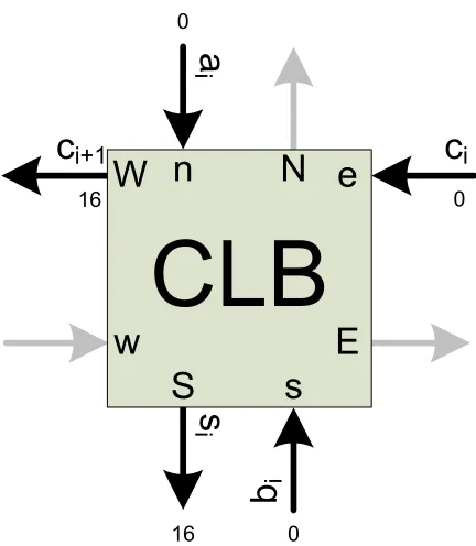
The proposed architecture for the FPGA is a cellular array of CLBs tiled together. Figure 3.1 demonstrates an example of the proposed FPGA. The number of CLBs tiled together determines the size of the applications that can be performed on the FPGA. Each side of a CLB block has a single input and a single output. The outputs of each CLB are connected to the adjacent CLB’s input for data communication purposes. Besides the input and output lines shown on the figure, there are also some configuration bits used to configure the CLB memory on the right side of the FPGA (not shown on the figure) and the output of those bits are on the left side of the FPGA.
CLB CLB CLB
CLB CLB CLB
CLB CLB CLB
Figure 3.1: Architecture for QCA FPGA.
3.2
CLB
The CLB is composed of fourlook-up tables (LUTs). The LUTs are placed
in a 2× 2 array to form the CLB. Figure 3.2 shows the block diagram of
the CLB. It has four data inputs: n, s, e, w, and four data outputs: N, S, E,
W. There are 16 additional configuration inputs to the CLB, which are not
shown on the Figure 3.2, but will be explained in Section 3.4. The four data inputs come from the four corners of the CLB and travel to the center. The signals are then evenly distributed to the four LUTs. Each input line must incur the same number of clock cycles of latency to ensure a throughput of one read operation per clock cycle. The CLB was first developed by [16], and then optimized by [32]. It takes seven clock cycles for the data to travel
from n, s, e, andw to the LUTs. Then each LUT takes nine clock cycles to
W n e w s S n w e s N s e w n E s w e n W n N e E s S w
Figure 3.2: Block diagram of CLB.
Verilog model using HDLQ [29] is separately developed. The completed simulations in both programs are shown in Chapter 4.
3.3
LUT
between each cell. This enables a throughput of one read per cycle. The to-tal latency from the decoded address to arrive at a valid output is nine clock cycles.
At the bottom right of the LUT, there is the output of the LUT. It is the OR of the enabled outputs of all 16 memory cells. The decoder ensures that only one memory cell is enabled. Thus, the output of the entire LUT is equal to the value stored in the enabled cell.
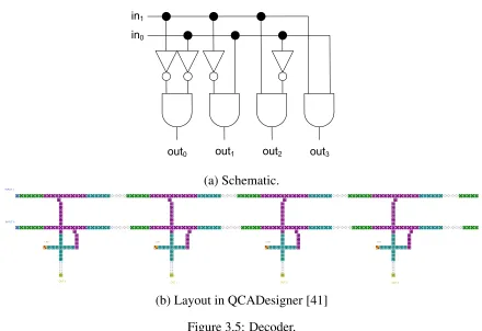
The decoder used in the LUT is similar to the traditional CMOS memory design, which has separate row and column decoders. This decoder is capa-ble of decoding four inputs to 16 outputs that matches with the 16-memory block in the design. Figure 3.5 shows the schematic and layout of the 2-to-4 decoder. The row and column decoders are identical to each other. The only difference is the rotation. The outputs of the row and column decoders are ANDed together to form the enable signals inside the memory blocks.
Figure 3.4 (b) shows the schematic of the LUT. The decoders are located
on the top and left side. The 16 cells in the middle are arranged in a 4 ×
4 array. The bottom right is the output circuitry that combines all the 16
memory outputs. To configure the LUT, there are four input lines for the memory entering from the right side, and there are also four input lines for a Read/Write (RW) signal entering from the left side. The device has a read latency of nine clock cycles and a throughput of one read operation per clock cycle. It is designed in a way that it is possible to rotate it and to connect it
to another LUT. Arranging four LUTs in a2×2array gives the CLB shown
in Figure 3.2.
3.3.1 Unit Memory
COLUMN DECODER UNIT MEM CELL UNIT MEM CELL UNIT MEM CELL UNIT MEM CELL UNIT MEM CELL UNIT MEM CELL UNIT MEM CELL UNIT MEM CELL UNIT MEM CELL UNIT MEM CELL UNIT MEM CELL UNIT MEM CELL UNIT MEM CELL UNIT MEM CELL UNIT MEM CELL UNIT MEM CELL R OW D E C OD E R OR GATE OR GATE OR GATE ONE CLOCK CYCLE DELAY
2 3 4 5
2 3 4 5 6
3 4 5 6 7
4 5 6 7 8
2
3
4
2 3 4
3 4 5 6
4 5 6 7
5 6 7 8
OUTPUT 9 1 1 0 0 0 0 (a) Schematic. 1.00 -1.00 -1.00 W_MC_0 -1.00
-1.00
1.00 -1.00 -1.00 W_MC_4 -1.00
-1.00
1.00
1.00 -1.00 -1.00 W_MC_1 -1.00
-1.00
1.00 -1.00 -1.00 W_MC_5 -1.00
-1.00 1.00 DI_OUT_0 WRITE_IN_0 B A -1.00 DI_OUT_1 WRITE_IN_1 -1.00 1.00 -1.00 -1.00 W_MC_2 -1.00
-1.00
1.00 -1.00 -1.00 W_MC_6 -1.00
-1.00
1.00
1.00 -1.00 -1.00 W_MC_3 -1.00
-1.00
1.00 -1.00 -1.00 W_MC_7 -1.00
-1.00 1.00 DI_OUT_2 WRITE_IN_2 -1.00 DI_OUT_3 WRITE_IN_3 -1.00 D C -1.00 -1.00 1.00 -1.00 -1.00 W_MC_8 -1.00
-1.00
1.00
1.00 -1.00 -1.00 W_MC_C -1.00
-1.00
1.00 DATA_IN_0
1.00 -1.00 -1.00 W_MC_9 -1.00
-1.00
1.00
1.00 -1.00 -1.00 W_MC_D -1.00
-1.00
1.00
1.00 -1.00 -1.00 W_MC_A -1.00
-1.00
1.00
1.00 -1.00 -1.00 W_MC_E -1.00
-1.00
1.00
1.00 -1.00 -1.00 W_MC_B -1.00
-1.00
1.00
1.00 -1.00 -1.00 W_MC_F -1.00
-1.00 1.00 -1.00 -1.00 DATA_IN_1 WR_OUT_1 1.00 DATA_IN_2 WR_OUT_2 1.00 DATA_IN_3 WR_OUT_3 1.00 OUT
(b) Layout in QCADesigner [41]
in1
in0
out0
out1 out2
out3
(a) Schematic. OUT 0 OUT 1 INPUT 1 INPUT 0 -1.00 -1.00 OUT 2 -1.00 OUT 3 -1.00
[image:41.612.89.529.83.385.2](b) Layout in QCADesigner [41]
Figure 3.5: Decoder.
cycle. One more important idea in the design is the way that memory is con-figured. Memory is only written when the RW signal encounters a pulse on the DI signal. Otherwise, the memory is not being configured and remains unchanged. The configuration process is discussed in Section 3.4.
3.3.2 Output Circuitry
The output circuitry merges the outputs from all the memory cells such that the enabled cell determines the output of the LUT. QCA does not have tris-tate buffers. Therefore, the use of logic for selecting a single output from the memory cells is required. The proposed LUT used a series chain of OR gates to achieve one read per clock cycle. The decoder and the output circuitry are arranged in a way that the input information and the output information flow in the same direction as each other. The proposed design ensures a fully pipelined operation. The design has similarity to that of [42]. However, the throughput frequency is unclear from [42].
Zone 3
Zone 0
Zone 1
Zone 2
Zone 3 Zone 0 Zone 1 Zone 2
Zone 3
Zone 3
(a) Schematic.
1.00 -1.00
-1.00 -1.00
DATA_OUT
-1.00
1.00
COL_IN
RW_IN ROW_IN
OR_IN
COL_OUT
DATA_IN ROW_OUT
RW_OUT
CELL_OUT
(b) Layout in QCADesigner.
Four OR chains are running horizontally, and one is running vertically. The horizontal chains combine the value stored in the memory within a row, and the vertical chain merges the values from four horizontal chains. Each OR chain is made up of three gates, and it is executed in parallel with the row and column decoders. This two-stage OR gate circuitry and the row and column decoders are designed specifically for selecting a single memory cell out of the 16-bits memory of the LUT. In Figure 3.7, besides the three OR gates on the vertical (rightmost chain), all other OR gates are embedded within the unit memory cell of Figure 3.6.
Figure 3.7 (b) shows the layout of the output circuitry. The latency of the OR chain is one clock cycle for a single OR operation. This is important because the row and column decoders also have the same latency to ensure a fully pipelined structure for the LUT. The delay along the OR chain matches the delay along the array of Figure 3.4 (a) for a throughput of one read operation per clock cycle.
3.4
Configuration
0 4 1 2 3 8 12
5 9 D
A E
6
7 B F
OUT (a) Schematic. OR_IN_0 1.00 ENABLE_4 OR_IN_1 1.00 ENABLE_5 OR_IN_2 1.00 ENABLE_6 OR_IN_3 1.00 ENABLE_7 1.00 ENABLE_8 1.00 ENABLE_C 1.00 ENABLE_9 1.00 ENABLE_D 1.00 ENABLE_A 1.00 ENABLE_E 1.00 ENABLE_B 1.00 ENABLE_F 1.00 1.00 1.00 OUTPUT (b) Layout.
Figure 3.8: A single CLB.
A CLB consists of four LUTs. Each LUT has 16 memory cells, which means a complete CLB has 64 bits of memory. Figure 3.9 shows how the memory is allocated in the CLB. Each DATA IN signal forms a pair with its matching RW signal. Each such pair controls an entire row of memory. Based on this type of configuration, to set up a desired function, a truth table must be written first. In Figure 3.9, the memory is divided into four sections.
The top right section is associated with the N output. The top left section is
associated with the W output. The bottom right section is associated with
theE output. Finally, the bottom left section is associated with theS output.
The input to the CLB block is in a (e, w, s, n) pattern. For example, when
an input of0111 is given to the CLB, the CLB must return the values stored
in the location of 7 in all four sections. Equations (3.1) and (3.2) show the
full adder logical behavior.
si = ai ⊕bi ⊕ci (3.1)
ci+1 = aibi+ bici+aici (3.2)
W N
15 11 7 3 3 7 11 15
14 10 6 2 2 6 10 14
13 9 5 1 1 5 9 13
12 8 4 0 0 4 8 12
12 8 4 0 0 4 8 12
13 9 5 1 1 5 9 13
14 10 6 2 2 6 10 14
15 11 7 3 3 7 11 15
S E
Figure 3.9: Position of each address within the LUT of the CLB.
port of the CLB. It is simple to match the truth table with memory config-uration. This table is set so that it increases its value from 0 to 15 in the binary system. The addresses in Table 3.1 correspond to the locations in
Figure 3.9. In this example, N and E are all meaningless (don’t care)
val-ues. Therefore, the memory associated with them, the top right and bottom
right sections, should be set to ‘0.’ si andci+1 correspond to the bottom left
and the top left sections. Those memory units must be configured as shown in Tables 3.2 and 3.3. Based on the setup and the memory configuration input from Figure 3.8, each DATA IN controls a row of memory. Table 3.4 shows the inputs needed to configure the CLB into a full adder. Between each valued input, there must be a delay cycle to match the RW signals. There are eight of memory units in each row, so eight valid inputs are re-quired to configure the memory unit. The first eight cycles from Table 3.4 configure the left part of the memory in the CLB. The last eight cycles
con-figure the right part of the memory in the CLB. In the table, X indicates a
don’t carebit. It is just because this full adder example does not require the
right part of memory to function. When users design their own functions, they will have to figure out the memory input for them. RW signals travel in
the opposite direction from that of theDAT A IN signals. Each RW signal
must have the input sequence of 0000000001000000. This sequence starts
the RW pulse with the correct timing to meet each bit of the DAT A IN at
the appropriate cell. Once the full adder is configured, the top left memory
contains EE88 in hex and bottom left contains 9966 in hex, and the other
Table 3.1: Full adder truth table.
Address Inputs Outputs
ci bi ai ci+1 si
e w s n W S N E
0 0 0 0 0 0 0 X X
1 0 0 0 1 0 1 X X
2 0 0 1 0 0 1 X X
3 0 0 1 1 1 0 X X
4 0 1 0 0 0 0 X X
5 0 1 0 1 0 1 X X
6 0 1 1 0 0 1 X X
7 0 1 1 1 1 0 X X
8 1 0 0 0 0 1 X X
9 1 0 0 1 1 0 X X
10 1 0 1 0 1 0 X X
11 1 0 1 1 1 1 X X
12 1 1 0 0 0 1 X X
13 1 1 0 1 1 0 X X
14 1 1 1 0 1 0 X X
15 1 1 1 1 1 1 X X
Table 3.2: si memory configuration.
1 1 0 0
0 0 1 1
0 0 1 1
1 1 0 0
Table 3.3: ci+1memory configuration.
1 1 1 1
1 1 0 0
1 1 0 0
Table 3.4: Input for configuration.
Input clock cycle 1 2 3 4 5 6 7 8 9 10 11 12 13 14 15 16
DAT A IN3 1 - 1 - 1 - 1 - X - X - X - X
-DAT A IN2 1 - 1 - 0 - 0 - X - X - X - X
-DAT A IN1 1 - 1 - 0 - 0 - X - X - X - X
-DAT A IN0 0 - 0 - 0 - 0 - X - X - X - X
-DAT A IN4 1 - 1 - 0 - 0 - X - X - X - X
-DAT A IN5 0 - 0 - 1 - 1 - X - X - X - X
-DAT A IN6 0 - 0 - 1 - 1 - X - X - X - X
-Chapter 4
Simulation and Analysis
Two different simulators, QCADesigner [41] and HDLQ [29] with
Model-Sim, are used for the simulation. The layout was first drawn and simulated
using QCADesigner. However, at the one-CLB level, the simulation time requires more than 12 hours. To reduce the significant amount of simula-tion time, HDLQ with ModelSim is used for designs with more than one CLB. All the architectures below the CLB level are rebuilt in HDLQ and simulated for verification. The results from both QCADesigner and HDLQ match each other. However, HDLQ is possible for large-scale simulation.
QCADesigner is an open-source software package that many QCA re-searchers have been using. However, QCADesigner simulator (V.2.0.3) was last updated at 2005. Although the tool allows simulating of multi-layer QCA, not enough evidence is provided to support the feasibility of such de-sign. Therefore, all the architectures presented in this thesis use a single layer. HDLQ [29] is a Verilog library for behavioral simulation of QCA architectures. Unlike QCADesigner, which models QCA at the physical level with quantum-mechanics, HDLQ models QCA circuits by assuming an ideal logical model of QCA operation. This is important for a fast proto-typing of complex QCA circuit. The complex QCA circuits are composed
of different logic blocks. For example, wire, fanout, inverter, andmajority
voter blocks are provided in the HDLQ library. The unit memory, LUT,
CLB, and FPGA are formed as structural interconnections of these blocks. In each level up to the CLB, the simulation results match those of QCADe-signer.
The CLB of Figure 3.3 is simulated in QCADesigner version 2.0.3 using
Figure 4.1: Full adder symbol.
number of samples is 300,000. All remaining parameters use the default values provided by QCADesigner.
4.1
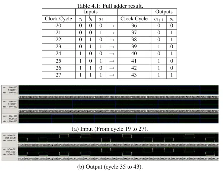
Full Adder
In the first step of design verification, the 1-bit full adder (FA) is simulated
using QCADesigner. The FA implements Equations (3.1) and (3.2). Fig-ure 4.1 shows the schematic view of the FA. FigFig-ure 3.3 shows the layout. In this circuit, inputs and outputs are given, as shown in Figure 4.1. Table 4.1 shows a general input and output relationship. Our CLB has a latency of 16 clock cycles, which means for any given input vector to the system, the cor-responding output is expected after 16 clock cycles. As for this full adder
testing, only three inputs, ai,bi, andci, are given. To run an exhaustive test,
eight test vectors are given to the system.
Table 4.1: Full adder result.
Inputs Outputs
Clock Cycle ci bi ai Clock Cycle ci+1 si
20 0 0 0 → 36 0 0
21 0 0 1 → 37 0 1
22 0 1 0 → 38 0 1
23 0 1 1 → 39 1 0
24 1 0 0 → 40 0 1
25 1 0 1 → 41 1 0
26 1 1 0 → 42 1 0
27 1 1 1 → 43 1 1
(a) Input (From cycle 19 to 27).
(b) Output (cycle 35 to 43).
Figure 4.2: FA simulation in QCADesigner.
the FA. IN N ORT H, IN SOU T H, and IN EAST are the three inputs:
ai, bi, andci. OU T SOU T H issi, andOU T W EST is ci+1.
Figure 4.3 demonstrates the input and output waveform in HDLQ. There is a signal named zone1 in the figure. It represents the clock provided to the cells in clock zone 1 of the QCA system. Only one clock is shown here because the output signal changes its status based on this clock. On Figure 4.3, each cycle is 100 ns with the exception of the first cycle being 75 ns to match the clock cycles in QCADesigner. These times are arbitrary. The actual clock period needed for correct operation would depend on the
physical QCA implementation used. data0 in0and data0 in1 are the two
input line used to configure the memory of the LUT. in a, in b, and in c
Figure 4.3: Simulation result of full adder in HDLQ. 32 48 0 0 16 16 c0 c1 a 0 s 0 b0 0 16 32 c2 a 1 s 1 b1 32 48 48 c3 a 2 s 2 b2 64 64 c4 a 3 s 3 b3 48 16 32 N W n e
S
E s w
N W n e
S
E s w
N W n e
S
E s w
N W n e
S
E s w
Figure 4.4: RCA block diagram.
larger-scale design, HDLQ is used to replace QCADesigner.
4.2
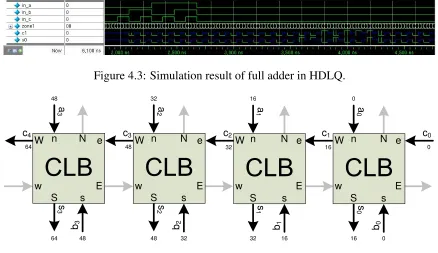
Ripple Carry Adder
A 4-bit ripple-carry adder (RCA) is constructed by tiling four 1-bit full
adders together. Figure 4.4 shows the block diagram of the design. The HDLQ Verilog model is simulated using ModelSim. To achieve a 4-bit plus 4-bit RCA, the FPGA is made up of four CLBs tiled together horizontally. For two 4-bit numbers, there are nine inputs to the system and five outputs from the system. Figure 4.4 shows how CLBs are tiled together to form
the 4-bit RCA. CLB0 is the least significant block. It takes three inputs, c0,
a0, and b0, to produce two outputs, c1, and s0. The behavior of the RCA
is calculated based on Equations (3.1) and (3.2), from which the expected output from each bit can be calculated.
As shown in Figure 4.4, CLB0 produces s0 and c1 for CLB1. CLB1
follows the same behavior for CLB2 and thenCLB3. The final five output
an exhaustive test set of all 512 input combinations. Figure 4.4 depicts four CLBs configured to implement the RCA. Within each shaded CLB, the
inputs are n, s, e, w, and the outputs are N, S, E, W. The function is then
determined by the memory configuration. The gray arrows in Figure 4.4 represent inputs to and outputs from the CLBs that are not used by the RCA design.
The number next to each signal on the figure indicates the clock cycles of latency relative to the initial inputs applied to the least significant bit. For
a given test vector, if a0, b0 and c0 are all applied at clock cycle t, then any
signal marked with the numbernin the diagram occurs at clock cyclet+n.
For an input signal, this means that the user must apply that input at the indicated cycle. For an output, this means that the output must be read at that cycle.
The latency on the critical path from the least-significant inputs to the most significant outputs is 64 clock cycles long. However, the adder is fully pipelined. Note that all the inputs to a given CLB arrive with the same latency. The least significant bits for the next pair of addends can be applied
in cycle t+ 1. Thus, a throughput of one addition per clock cycle can be
maintained. Figure 4.5 shows the partial waveform result from HDLQ.
Here is an example of the addition process. If 0111 + 1110 are given
to the RCA, Table 4.2 shows the input and output sequences of the RCA.
The inputs need to be staggered. That is why 0111 and 1110 are split and
given to the RCA in four different clock cycles, and there are also four
outputs associated with each given input after 16 clock cycles. The Xs in
the table are the do not care bits. Table 4.2 only shows one addition process. However, it does not mean that the clock cycles in between are idle. Those clock cycles in between are also calculating other sets of addition process.
Calculating the exact number of cycles for a signal to arrive at certain
time seems like a wave pipeline. Wave pipelining is to send in a steam of
(a) Cycle 189 to 221.
[image:54.612.94.528.191.573.2](b) Cycle 222 to 254.
Table 4.2: RCA result.
Clock Cycle Input Bit Carry Bit Output Bit
190 a0 = 1,b0 = 0,c0= 0
206 a1 = 1,b1 = 1,c0= 0 c1 = 0 s0 = 1
222 a2 = 1,b2 = 1,c0= 0 c2 = 1 s1 = 0
238 a3 = 0,b3 = 1,c0= 0 c3 = 1 s2 = 1
254 c4 = 1 s3 = 0
In this sense, a QCA circuit operates as a wave pipeline. In the test bench design, all the inputs are pre-designed and sent into the system like a wave of signals. The complete simulation waveform of the RCA can be found in Appendix B.
To run an exhaustive test on the 4-bit RCA requires a long list of vectors. To avoid mistakes in the test bench, a spreadsheet is used to compute the inputs and expected outputs. After the results are constructed, each input is staggered according to the CLB latencies. The table is saved into a text file. This file contains the input to the system and also the expected output from the system in each cycle. The test bench is able to read from this file, so it knows in which cycle what inputs are given to the RCA and what outputs are expected. The test bench compares the actual outputs from the RCA with the expected outputs from the text file. If there is mismatch from the comparing process, the mismatch cycle is reported on the screen.
4.3
Bit-Serial Multiplier
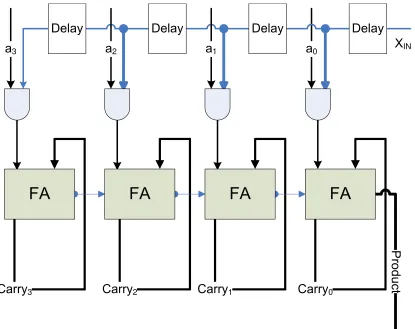
Another application for the proposed FPGA is abit-serial multiplier(BSM).
The BSM is capable of taking two 4-bit numbers and multiplying them
to-gether. Figure 4.6 shows the block diagram of the BSM.A = ha3, a2, a1, a0i
is the multiplicand and is input to the system in parallel. XIN represents
one bit of the multiplier from X = hx3, x2, x1, x0i and is input serially
two 4-bit factors, 256 cycles are needed. The design is tested under HDLQ with ModelSim. The test bench was written to compare the simulation out-put to the expected outout-put from the file. To run an exhaustive test, 65,536 test vectors are needed. The simulation results match to the expected result. Therefore, the proposed FPGA is proven to handle BSM. Partial waveform results are shown in Appendix C.
BSM is chosen to be one of the test applications because of the delays in the design. The proposed CLB is a heavy pipelined structure. Initially, the array multiplier seems to be a good application for the proposed CLB because of the pipelined block structure. However, it turns out that the signal cannot always arrive at desired time because different paths between the same two points can have different latencies. The internal delay makes the array multiplier hard to implement using the proposed FPGA. Instead BSM has a lot of internal signal delays, which fits to the delay of the proposed
CLB. 12 CLBs in an array format of3×4are used to implement the BSM.
Each CLB in the middle row is configured to be a 1-bit full adder. Each
CLB in the top row is configured as an AND gate for ANDing ai andXIN.
In Figure 4.6, there are many delay boxes shown on the schematic. Those delays can be taken care by the proposed CLB internal delay. Each CLB in the bottom row is configured to be a feedback loops.
4.4
Glitchless Reconfiguration
Partial reconfiguration [33, 45] is a process to configure part of an FPGA
while the whole FPGA is still operating. Partial reconfiguration is interest-ing in many areas. Patterson [31] applied the partial reconfiguration
tech-nique to the data encryption standard (DES) algorithm. DES is a private
key algorithm that is used to encrypt or decrypt the information transferred. The FPGA implementation uses a circuit that is specialized for a particu-lar key to improve performance. Patterson uses partial reconfiguration to replace the key-specific portion of the circuit leaving the rest unchanged.
0 2
3 1
3 2 1 0
[image:57.612.97.512.196.525.2]IN
FPGA, this unit consists of one row of configuration bits. Therefore, par-tially reconfiguring a region that does not span the full width of the device requires reconfiguring areas on either side of the target region. In these ar-eas, the new configuration bits are equal to the old configuration bits. If the user circuits in the side region are to keep operating uninterrupted during partial reconfiguration, it is important that this operation does not cause a glitch in any configuration values in the side regions. An FPGA is said to
support glitchless reconfiguration if, when a bit holds the same value
be-fore and after reconfiguration, the act of reconfiguration is guaranteed not to cause a glitch [33].
Figure 4.7 shows the result of glitchless reconfiguration from QCADe-signer. It uses the same example of a 1-bit full adder. Table 4.3 shows the
inputs and memory results with clock cycles. Data IN3...0 andData IN7...4
are used to configure the memory. It needs 17 cycles to configure the 8×8
memory of the proposed CLB. Cycle 1 to 17 from Table 4.3 shows the vec-tors to configure the memory to emulate the CLB. The address inputs are given when the configuration process is completed. However, to observe the
reconfiguration process, Data IN3...0 and Data IN7...4 are given the same
Table 4.3: Glitchless reconfiguration.
Cycle Data IN3...0 Data IN7...4 RW IN Address input NM C EM C
1 E 9 0 0 zzzz zzzz
2 - - 0 0 zzzz zzzz
3 E 9 0 0 zzzz zzzz
4 - - 0 0 zzzz zzzz
5 8 6 0 0 zzzz zzzz
6 - - 0 0 zzzz zzzz
7 8 6 0 0 zzzz zzzz
8 - - 0 0 zzzz zzzz
9 - - 0 0 zzzz zzzz
10 - - 1 0 zzzz zzzz
11 0 0 0 0 zzzz zzzz
12 - - 0 0 Ezzz 9zzz
13 0 0 0 0 EEzz 99zz
14 - - 0 0 EE8z 996z
15 0 0 0 0 EE88 9966
16 - - 0 0 EE88 9966
17 0 0 0 0 EE88 9966
18 - - 0 0 EE88 9966
19 - - 0 0 EE88 9966
20 E 9 0 0 EE88 9966
21 - - 0 1 EE88 9966
22 E 9 0 2 EE88 9966
23 - - 0 3 EE88 9966
24 8 6 0 4 EE88 9966
25 - - 0 5 EE88 9966
26 8 6 0 6 EE88 9966
27 - - 0 7 EE88 9966
28 - - 0 0 EE88 9966
29 - - 1 1 EE88 9966
30 - - 0 2 EE88 9966
31 0 0 0 3 EE88 9966
32 - - 0 4 EE88 9966
33 0 0 0 5 EE88 9966
34 - - 0 6 EE88 9966
Figure 4.7: Simulation result of glitchless reconfiguration.
Table 4.4: Full adder result during partial reconfiguration.
Inputs Outputs
Clock Cycle ci bi ai Clock Cycle ci+1 si
20 0 0 0 → 36 0 0
21 0 0 1 → 37 0 1
22 0 1 0 → 38 0 1
23 0 1 1 → 39 1 0
24 1 0 0 → 40 0 1
25 1 0 1 → 41 1 0
26 1 1 0 → 42 1 0
27 1 1 1 → 43 1 1
28 0 0 0 → 44 0 0
29 0 0 1 → 45 0 1
30 0 1 0 → 46 0 1
31 0 1 1 → 47 1 0
32 1 0 0 → 48 0 1
33 1 0 1 → 49 1 0
34 1 1 0 → 50 1 0
Chapter 5
Conclusions and Future Work
This thesis presents the design, layout and successful simulation of a LUT-based CLB in QCADesigner and HDLQ. A collection of four CLBs and another collection of 12 CLBs acting as a very simple FPGA are also sim-ulated in HDLQ. Previous work on FPGAs in QCA has focused on pro-grammable interconnect. In contrast, this thesis presents what we believe to
be the first QCA design to use multiple CLBs consisting of look-up tables
(LUTs).
QCA depends on the use of clocks throughout. Even logic gates and wires are clocked. Thus, even simple operations incur multiple clock cycles of latency. This forms a fundamental design challenge in QCA. To achieve high throughput, QCA designs must be heavily pipelined. The LUTs pre-sented here adopt a two-dimensional memory structure with separate row and column decoders inspired by CMOS memories. These are carefully de-signed such that inputs and outputs all flow in the same direction and delays are matched. This allows the LUTs to maintain a throughput of one trans-action per clock cycle. The proposed CLB has just over half the area and incurs just over half the latency of the CLB of [16].
We have demonstrated a sample application of a four-bit ripple-carry adder (four-CLB) and a four-bit bit serial multiplier (12-CLB) running on the simple FPGA. Although the latency of the critical path is 64 clock cy-cles, the adder maintains a throughput of one sum per clock cycle. This is achieved by applying the same strategy as that used to design the LUT.
memory is configured [16, 36]. Although the reconfiguration bits are input serially, they are not shifted from cell to cell. Instead, each bit only changes the value of its destination cell.
Once more realistic applications are implemented, we will be in a better position to compare the effectiveness of configurable logic to that of config-urable routing in the context of QCA. The FPGA presented here relies en-tirely on configurable logic. Most commercial FPGAs use both configurable logic and configurable routing. Possible future work could investigate com-bining our CLB with configurable routing of existing QCA designs.
Currently, all the applications presented here rely on hand-mapping for all the memory allocation, which takes time and has a high possibility of
error. To reduce the error and time, anelectronic-design automation (EDA)
tool must be developed to efficiently map applications to our design.
An issue in the proposed FPGA design is that the function cannot always have matched latency from every signal. QCA is a pipelined technology. Hence, everything must be pipelined. The CLB presented in this thesis maintains a throughput of one transaction per clock cycle. However, in a user design, different paths might cross different numbers of CLBs before converging. Such mismatch delays interfere with pipelining. This issue has been studied in other fields [35, 44]. In those papers, the proposed FPGA
is considered as fixed-frequency FPGA. They proposed an idea to solve this
issue by adding a programmable delay at the input or output of each CLB to balance the path delays. Further research can apply the techniques of [35, 44] to the CLB presented in this thesis.
Bibliography
[1] Alan Allan, Don Edenfeld, William H. Joyner, Jr., Andrew B. Kahng,
Mike Rodgers, and Yervant Zorian. 2001 technology roadmap for
semiconductors. IEEE Computer, 35(1):42–53, 2002.
[2] M. A. Amiri, M. Mahdavi, and S. Mirzakuchaki. QCA implementation
of a mux-based FPGA CLB. InProceedings of the International
Con-ference on Nanoscience and Nanotechnology (ICONN 2008), pages
141–144, February 2008.
[3] Adrian Bachtold, Peter Hadley, Takeshi Nakanishi, and Cees
Dekker. Logic circuits with carbon nanotube transistors. Science,
294(5545):1317–1320, 2001.
[4] Gary H. Bernstein. Quantum-dot cellular automata: computing by
field polarization. InDAC ’03: Proceedings of the 40th annual Design
Automation Conference, pages 268–273. ACM, 2003.
[5] Gary H. Bernstein, Alexandra Imre, V. Metlushko, Alexei O. Orlov,
L. Zhou, L. Ji, Gy¨orgy Csaba, and Wolfgang Porod. Magnetic QCA
systems. Microelectronics Journal, 36(7):619–624, 2005.
[6] Stephen Brown and Jonathan Rose. FPGA and CPLD architectures: A
tutorial. IEEE Des. Test. Comput., 13(2):42–57, 1996.
[7] Stephen Brown and Zvonko Vranesic. Fundamentals of Digital Logic
with VHDL Design. McGraw-Hill Higher Education, third edition,
[8] B. H. Calhoun, Yu Cao, Xin Li, Ken Mai, L. T. Pileggi, R. A. Rutenbar,
and K. L. Shepard. Digital circuit design challenges and opportunities
in the era of nanoscale CMOS. Proc. IEEE, 96(2):343–365, February
2008.
[9] Tze-Chiang Chen. Where CMOS is going: trendy hype vs. real
tech-nology. InProceedings of the IEEE International Solid-State Circuits
Conference (ISSCC 2006), pages 1–18, February 2006.
[10] R. P. Cowburn and M. E. Welland. Room temperature magnetic
quan-tum cellular automata. Science, 287(5457):1466–1468, 2000.
[11] R.P. Cowburn. Digital nanomagnetic logic. In Device Research
Con-ference, pages 111–114, June 2003.
[12] Yi Cui and Charles M. Lieber. Functional nanoscale electronic
de-vices assembled using silicon nanowire building blocks. Science,
291(5505):851–853, 2001.
[13] S. Anisul Haque, Masahiko Yamamoto, Ryoichi Nakatani, and Yasushi
Endo. Magnetic logic gate for binary computing. Science and
Technol-ogy of Advanced Materials, 5(1-2):79 – 82, 2004. 21st Century COE
Program, Osaka University.
[14] A. Imre, G. Csaba, L. Ji, A. Orlov, G. H. Bernstein, and W. Porod.
Ma-jority logic gate for magnetic quantum-dot cellular automata. Science,
311(5758):205–208, 2006.
[15] A. Jazbec, N. Zimic, I. L. Bajec, P. Pe˘car, and M. Mraz. Quantum-dot
field programmable gate array: enhanced routing. In Proceedings of
the 2006 Conference on Optoelectronic and Microelectronic Materials
[16] Timothy D. Lantz and Eric R. Peskin. A QCA implementation of a
configurable logic block for an FPGA. In Proceedings of the Third
International Conference on Reconfigurable Computing and FPGAs
(ReConFig 2006), pages 132–141, September 2006.
[17] C. S. Lent and P. D. Tougaw. A device architecture for computing with
quantum dots. Proc. IEEE, 85(4):541–557, April 1997.
[18] C. S. Lent, P. D. Tougaw, W. Porod, and G. H. Bernstein. Quantum
cellular automata. Nanotechnology, 4(1):49–57, January 1993.
[19] Craig S. Lent, Beth Isaksen, and Marya Lieberman. Molecular
quantum-dot cellular automata. Journal of the American Chemical
Society, 125(4):1056–1063, January 2003.
[20] Craig S. Lent, P. Douglas Tougaw, and Wolfgang Porod. Bistable
satu-ration in coupled quantum dots for quantum cellular automata.Applied
Physics Letters, 62(7):714–716, 1993.
[21] Mo Liu and C. S. Lent. High-speed metallic quantum-dot cellular
au-tomata. In Proceedings of the Third IEEE Conference on
Nanotech-nology (IEEE-NANO 2003), volume 2, pages 465–468, August 2003.
[22] Fabrizio Lombardi, Jing Huang, Xiaojun Ma, Mariam Momenzadeh,
Marco Ottavi, Luca Schiano, and Vamsi Vankamamidi. Design and
Test of Digital Circuits by Quantum-Dot Cellular Automata. Artech
House, 2008.
[23] Yuhui Lu and C. S. Lent. Theoretical study of molecular quantum
dot cellular automata. In Proceedings of the 10th International
Work-shop on Computational Electronics (IWCE-10), pages 118–119,
[24] Yuhui Lu, Mo Liu, and Craig Lent. Molecular quantum-dot cellular
automata: From molecular structure to circuit dynamics. Journal of
Applied Physics, 102(3):034311, 2007.
[25] Gordon E. Moore. Cramming more components onto integrated
cir-cuits. Electronics, 38(8):114 ff., April 1965.
[26] Michael Thaddeus Niemier and Peter M. Kogge. The ‘4-diamond
cir-cuit’ - a minimally complex nano-scale computational building block
in QCA. In Proceedings of the IEEE Computer Society Annual
Sym-posium on VLSI (ISVLSI 2004), pages 3–10. IEEE Computer Society,
February 2004.
[27] Michael Thaddeus Niemier, Arun Francis Rodrigues, and Peter M.
Kogge. A potentially implementable FPGA for quantum dot
cellu-lar automata. In Proceedings of the First Workshop on Non-Silicon
Computation (NSC-1), pages 38–45, 2002.
[28] Alexei O. Orlov, Islamshah Amlani, Geza Toth, Craig S. Lent, Gary H.
Bernstein, and Gregory L. Snider. Correlated electron trans