Rochester Institute of Technology
RIT Scholar Works
Theses Thesis/Dissertation Collections
6-2015
An Interconnection Architecture for Seamless Inter
and Intra-Chip Communication Using Wireless
Links
Jagan Muralidharan [email protected]
Follow this and additional works at:http://scholarworks.rit.edu/theses
This Thesis is brought to you for free and open access by the Thesis/Dissertation Collections at RIT Scholar Works. It has been accepted for inclusion
in Theses by an authorized administrator of RIT Scholar Works. For more information, please [email protected].
Recommended Citation
An Interconnection Architecture for Seamless Inter and
Intra-Chip Communication Using Wireless Links
by
Jagan Muralidharan
A Thesis Submitted in Partial Fulfillment of the Requirements for the Degree of Master of Science in Computer Engineering
Supervised by
Dr. Amlan Ganguly
Department of Computer Engineering Kate Gleason College of Engineering
Rochester Institute of Technology Rochester, NY
June 2015
Approved By:
_____________________________________________ ___________ ___
Dr. Amlan Ganguly
Primary Advisor – R.I.T. Dept. of Computer Engineering
_ __ ___________________________________ _________ _____
Dr. Andres Kwasinski
Secondary Advisor – R.I.T. Dept. of Computer Engineering
_____________________________________________ ______________
Dr. Reza Azarderakhsh
ii
Dedication
I would like to dedicate this thesis to my parents Mr. Muralidharan and Mrs. Soundaravalli
who have supported me from the beginning of this journey. I would also like to dedicate
this to my mentor and all my friends who have been a great source of motivation and
iii
Acknowledgements
I take this opportunity to express my profound gratitude and deep regards to my primary
advisor Dr. Amlan Ganguly for his exemplary guidance, monitoring and constant
encouragement throughout this thesis. Dr. Ganguly dedicated his valuable time to review
my work constantly and provide valuable suggestions which helped in overcoming many
obstacles and keeping the work on the right track. I would also like to express my deepest
gratitude to Dr. Andres Kwasinski and Dr. Reza Azarderakhsh for sharing their thoughts
and suggesting valuable ideas which have had significant impact on this thesis. I am
grateful for their valuable time and cooperation during the course of this work. I also take
this opportunity to thank my research group members for all the constant support and help
iv
Abstract
As semiconductor technologies continues to scale, more and more cores are being
integrated on the same multicore chip. This increase in complexity poses the challenge of
efficient data transfer between these cores. Several on-chip network architectures are
proposed to improve the design flexibility and communication efficiency of such multicore
chips. However, in a larger system consisting of several multicore chips across a board or
in a System-in-Package (SiP), the performance is limited by the communication among
and within these chips. Such systems, most commonly found within computing modules
in typical data center nodes or server racks, are in dire need of an efficient interconnection
architecture.
Conventional interchip communication using wireline links involve routing the
data from the internal cores to the peripheral I/O ports, travelling over the interchip
channels to the destination chip, and finally getting routed from the I/O to the internal cores
there. This multihop communication increases latency and energy consumption while
decreasing data bandwidth in a multichip system. Furthermore, the intrachip and interchip
communication architectures are separately designed to maximize design flexibility.
Jointly designing them could, however, improve the communication efficiency
significantly and yield better solutions.
Previous attempts at this include an all-photonic approach that provides a unified
inter/intra-chip optical network, based on recent progress in nano-photonic technologies.
Works on wireless inter-chip interconnects successfully yielded better results than their
v
connection between two chips rather than a communication architecture for a system as a
whole.
In this thesis, the design of a seamless hybrid wired and wireless interconnection
network for multichip systems in a package is proposed. The design utilizes on-chip
wireless transceivers with dimensions spanning up to tens of centimeters. It manages to
seamlessly bind both intrachip and interchip communication architectures and enables
direct chip-to-chip communication between the internal cores. It is shown through cycle
accurate simulations that the proposed design increases the bandwidth and reduces the
energy consumption when compared to the state-of-the-art wireline I/O based multichip
vi
Table of Contents
Dedication ... iiAcknowledgements ... iii
Abstract ... iv
Table of Contents ... vi
List of Figures ... viii
List of Tables ... ix
Chapter 1 Introduction ...1
1.1. Network-on-Chip (NoC)... 1
1.2. Interchip Communication ... 4
1.3. Emerging Interconnect Architectures ... 6
1.4. Thesis Contribution ... 7
Chapter 2 Related Work ...10
Chapter 3 Wireless Multichip Architecture ...13
3.1. Topology ... 14
3.1.1 Multichip System with Intrachip Mesh ... 14
3.1.2 Multichip System with Intrachip Small-World ... 15
3.2. Physical Layer ... 17
3.3. Wireless Communication Protocol ... 18
3.4. Routing ... 20
Chapter 4 Simulation Results ...22
vii
4.2. Wireless Link Budget Analysis ... 24
4.3. Performance Evaluation ... 25
4.3.1 Achievable Bandwidth ... 27
4.3.2 Packet Energy ... 29
4.4. Performance Evaluation with Non-Uniform Traffic ... 31
4.5. Area Overheads ... 35
Chapter 5 Conclusions and Future Work ...37
viii
List of Figures
Fig. 1: Network-on-Chip Architecture [4] ... 2Fig. 2: Range of different interconnection architectures ... 5
Fig. 3: Architecture of the proposed wireless multichip system ... 13
Fig. 4: Small-World NoC architecture with short and long range links [29] ... 16
Fig. 5: Block diagram of mm-wave CDMA based wireless transceiver ... 19
Fig. 6: Peak achievable bandwidth per core for varying system size, for uniform traffic ... 28
Fig. 7: Average packet energy dissipation with varying system size, with uniform traffic ... 30
Fig. 8(a): Peak achievable bandwidth per core with non-uniform traffic (b): Packet Energy with non-uniform traffic ... 32
Fig. 9(a): Peak Bandwidth per core for 2 chip system with localization (b) Average packet energy for 2 chip system with localization ... 34
ix
List of Tables
1
Chapter 1
Introduction
In order to keep up with the growing performance demands of applications, modern
computing systems are becoming increasingly complex. The number of cores integrated
on a single chip is increasing, and the number of transistors have increased to billions. With
this increase comes the problem of communication delay among the cores. The electrical
wires that carry signals across the chip do not scale in length with technology, and hence
end up increasing the global wire delay. If this data latency becomes too large, the
processing cores would waste a lot of power being idle and by waiting [1].
Traditionally, ad-hoc and bus-based architectures were used for intra-chip
communication. These architectures, although seemingly adequate, worked well only for a
few number of cores. As the number of cores increased, the length of the shared bus would
also have to increase, leading to a high intrinsic parasitic capacitance and thus, increased
propagation delays. Moreover, the bandwidth available to each core reduced, resulting in
lower throughput and increased contention delays. This led to the introduction of ad-hoc
based architectures where the bus was split into multiple segments and employed
hierarchically [2]. However, this architecture still possessed the inherent limitations of the
bus-based architecture. In other words, the traditional architectures were not scalable to
higher number of cores on a chip. Thus, modern communication networks gradually moved
towards Network-on-Chip (NoC) architectures as a solution to the above problem [3].
1.1.
Network-on-Chip (NoC)
Network-on-Chip paradigm is a new approach of designing a scalable
2
approach where the communication infrastructure is separated from the functionality of the
cores. That is, this approach separates the communication network from the processing
elements and the data is routed over this network using intelligent switches or routers [4].
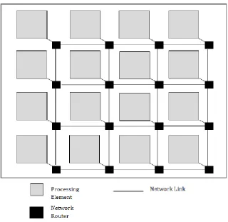
[image:12.612.164.484.210.521.2]Such an approach provides a scalable plug-and-play system, and facilitates reusability.
Fig.1 depicts a basic Network-on-Chip architecture for a 16 core system.
Fig. 1: Network-on-Chip Architecture [4]
Conventionally, there are three types of switching mechanisms used for data
routing in NoCs, namely Circuit Switching, Packet Switching and Wormhole Switching.
In circuit switched networks, a dedicated path is reserved for the entire transmission
3
the number of cores increases because there are numerous other cores waiting for
transmission along the same path. Hence this method is inefficient for larger systems. In
case of packet switched networks, the data is divided into packets and then each packet is
routed over the network. Since there is no reservation path in this case, the packets need to
be buffered in the switches along the path to the destination. This demands more area
overhead for the multicore System-on-Chip, which is not favorable.
Considering the drawbacks of the above two switching techniques, wormhole
switching is adopted in this work [5]. Here, the data packets are broken down into small
units called flow control units or flits. The size of each flit is chosen such that a single flit
can traverse a single hop in a single clock cycle. These flits are routed over the network
using switches, and each switch only forwards the first flit or the header flit onto the next
switch in the path to the destination. The rest of the flits (body flits) follow this path setup
by the header flit in pipelined fashion. Hence each switch only has to hold or forward these
smaller sized flits, eliminating the need for large buffers. However, reserving a path for a
particular packet would prevent other messages from being sent to a switch until the packet
is completely transmitted. As a solution, the concept of virtual channels is used where a
virtual path is reserved for each distinct message. Each packet being transmitted is
allocated a distinct buffer at each of the switches along its path to the destination. This way,
every packet gets a distinct virtual path, and each switch can send and receive packets from
4
1.2.
Interchip Communication
Large complex systems such as servers and datacenters encompass computing
modules with multiple multicore chips. In these environments, the lower level cache is
physically distributed between the cores, and cache or memory access would often require
communication between the cores of different chips. As the number of multicore chips
keeps scaling up in these systems, the interconnection between them is becoming
increasingly complex. Hence, in these infrastructures, the communication efficiency
among and within the chips is very important for the overall system performance.
While intrachip communication is gradually advancing to Network-on-Chip
architectures, interchip communication is also evolving at a rapid pace. For interchip
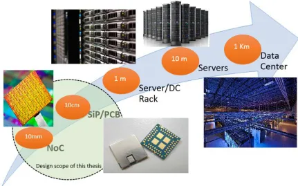
communications, bus-based and ad-hoc architectures are still popular, and signals are
mostly transmitted by electrical interconnects on printed circuit boards [13] [22]. In
multichip environments within a System-in-Package (SiP), solder bumps or C4
interconnects are used, spanning 10 mm in range. For board level multichip modules,
Peripheral Component Interconnect (PCI) is the most common local I/O bus technology
for interchip interconnection. Recently the PCI Express (PCIe) is presented as the next
generation I/O technology [6]. On a larger scale, when dealing with distances of several
meters to a kilometer such as in a datacenter warehouse, Ethernet cables are used for the
same interchip communication. Fig. 2 shows the range of different interconnection
5
Fig. 2: Range of different interconnection architectures
However, there is a huge performance gap between the interchip I/O and the
on-chip electrical interconnects. For instance, the limited number of I/O and the crosstalk
issues severely limit the bandwidth of interchip communication. The substantial difference
in physical lengths, resistance and capacitance between the I/O and the intrachip
interconnects account for the much larger interchip delay. Furthermore, the off-chip I/O
with high capacitance would require much larger drive power when compared to the
on-chip interconnects. These factors make interon-chip and intraon-chip interconnects mismatched,
and the two architectures are always designed with different protocols and properties [7].
Owing to this difference, the data from cores located within the chips need to travel to the
peripheral I/O blocks, traverse the interchip link, and then get routed over to its final
6
cores of a multichip system is highly inefficient in terms of energy consumption, latency
and bandwidth.
1.3.
Emerging Interconnect Architectures
In order to alleviate the problems of traditional off-chip interconnections, many
works have been proposed over the years. Optical interconnects are proposed as a
promising solution, to replace both inter- and intrachip electrical wires and interconnect
the two channels [7]. However, in spite of boasting advantages of ultrahigh throughput,
low delay and low power consumption, the pitch of photonic interconnects do not scale
well due to the limitations in size of silicon-photonic devices. Furthermore, manufacturing
the electronic components required for such a photonic interconnection is not feasible with
standard CMOS processes. Another promising solution is the proposition of vertically
integrated 3D ICs [8] which contain multiple layers of active devices. However, this
architecture requires extremely precise wafer-to-wafer alignment during manufacturing,
and sophisticated thermal management techniques.
Wireless links for data communication is a rising methodology and a good
alternative to traditional interconnects. As conventional metallic interconnects become the
bottleneck of Network-on-Chips, wireless NoC architectures are proposed [9], which
significantly improves the energy efficiency and bandwidth of on-chip data
communication. This method utilizes wireless links in the millimeter-wave (mm-wave)
bands using on-chip antennas embedded in the chip [10]. Recent research has shown that
these on-chip wireless interconnects is scalable to off-chip communication as well. These
7
multi GigaHertz bandwidths [10] [11]. In this case, the factors that posed major challenges
with traditional I/O are overcome here. For example, the delay difference between on-chip
and off-chip wireless interconnects is negligible owing to the high speeds of
electromagnetic waves. Also, the increase in power for increase in transmission length is
not as profound as with the wired interconnects. These factors make wireless interconnects
suitable for an alliance of inter- and intrachip architectures for multicore chips.
1.4.
Thesis Contribution
In this thesis, it will be shown that wireless interconnects can be used to establish a
seamless communication infrastructure for multichip systems within a single package. This
architecture will enable exchange of data between cores in a single chip as well as between
cores from different chips in a multichip system, thus seamlessly merging both the
interchip and the intrachip networks. The wireless links will span distances up to a few tens
of centimeters, using the same communication protocols for both interchip and intrachip
data transfer. Wireless transceivers will be integrated in a select few cores in the chips, and
each of these cores will be able to communicate directly with other such cores in a single
hop, within the same or different chips. To be equipped with these wireless transceivers,
the internal cores of the chips will be efficiently selected such that, on an average, every
other core will be within a short distance from its nearest transceiver. This will reduce
multihop communication and improve energy efficiency. This proposed work will
elaborate the design methodologies of two different interconnection architectures for such
a multichip System-in-Package. The work will also demonstrate how the design
8
The following points will summarize the contributions made during this work.
Proposed Interconnection Architecture
o Development of a methodology for seamless interconnection between
on-chip and off-chip data transfer
o Design of a seamless hybrid wired and wireless interconnection network
for multichip Systems-in-Packages
Evaluation of Wireless Multichip Architecture
o Evaluation of peak achievable bandwidth of the multichip network for
varying system size
o Evaluation of packet energy dissipation of the multichip network for
varying system size
o Analysis of bandwidth and packet energy for the multichip system with
non-uniform traffic patterns
o Comparison of performance metrics of the proposed wireless multichip
architecture with its wireline counterpart
Development of simulation framework
o Develop a cycle accurate simulator to implement the wireless multichip
architecture and monitor the progress of flits over the switches and links
per cycle
o Include the power consumption parameters of both the wired and
wireless links in the simulator to model the energy consumption in data
9
o Obtain experimental results of the wireless multichip architecture in
terms of the following metrics for performance evaluation:
Peak achievable bandwidth per core
Packet energy dissipation
Publication
o Md. Shahriar Shamim, Jagan Muralidharan and Amlan Ganguly, “An
Interconnection Architecture for Seamless Inter and Intra-Chip
Communication Using Wireless Links”, In Proceedings of International
10
Chapter 2
Related Work
The performance of on-chip and off-chip interconnections are significantly
mismatched since, according to the International Technology Roadmap for
Semiconductors (ITRS), the pitch of the interchip I/O interconnects is not scaling as fast
as the pitch of the on-chip interconnects [12]. Owing to this reason, interchip and intrachip
communication architectures are separately designed with different protocols and
properties.
For intrachip communication, traditionally, the cores communicated using a shared
bus based interconnection, which then gave way to a slightly more efficient bus splitting
methodology [13]. Current System-on-Chip (SoC) designs, however, are moving on to
Network-on-Chip (NoC) architectures to alleviate issues including poor scalability and
limited bandwidth. Here the functionality of the cores is separated from the communication
fabric by providing a dedicated infrastructure for data transmission. There have been
different types of architectures suggested in this regard, notably the SPIN (Scalable,
Programmable, Integrated Network) architecture where a fat-tree structure is used [14], the
mesh-based architecture called CLICHÉ (Chip-Level Integration of Communicating
Heterogeneous Elements) [15], the 2D-Torus architecture with wrap-around channels [3],
the OCTAGON interconnect architecture [16], the Butterfly Fat-Tree (BFT) architecture
[17], etc.. These NoC architectures are characterized with respect to their performance and
design trade-offs in [9], and shown how these trade-offs affect a typical multiprocessor
system performance. While NoC architectures improve the performance of SoCs, the
11
the conventional wired interconnects remain a bottleneck of NoC. Long range
high-bandwidth on-chip wireless data links are proposed as an energy efficient alternative [18]
where the multihop wired paths between distant cores are replaced by a single wireless
communication link. On-chip antennas from graphene or Carbon Nanotube based
structures are predicted to provide high bandwidth wireless communication channels [19]
[20]. However, integration of these antennas with standard CMOS processes needs to
overcome significant challenges, while mm-wave CMOS transceivers operating in the
sub-THz frequency ranges is a more near term solution. For intrachip and interchip
communication, mm-wave wireless on-chip embedded antennas are designed and
evaluated in [10]. For this wireless NoC (WiNoC) architectures, the medium access
mechanisms range from simple token passing protocols [9], to more sophisticated CDMA
based mechanisms [21].
For interchip communication, bus based architectures are still popular, and signals
are mostly transmitted by wired interconnects on printed circuit boards (PCB).
Conventionally, for a multichip system-in-package, C4 bumps coupled with in-package
transmission lines are used to interconnect chips [22]. On the board level, a scalable and
low power I/O transceiver is proposed in [23] which provides speeds of 5 to 15 Gbps over
single-board channels. For wireless interchip communication, [24] proposes a wirelessly
connected multichip module for a High Performance Computing environment. In [25]
on-chip wireless transceivers are used to facilitate fast prebonding wafer testing enabled by
direct access to components under test within the ICs. Wireless transceivers for 60 GHz
interchip and intrachip communications are designed in [26]. On a larger scale, a wireless
12
proposed to eliminate the performance issues of conventional I/O interconnects between
chips include [34] in which optical through-chip buses for thinned stacked dies are used
for interchip communication in SiPs. Also, [35] includes optical interconnections where
optical leaky-wave nano-antennas are used for data communication, and [7] uses optical
networks to jointly integrate both interchip and intrachip networks. In this thesis, a hybrid
inter and intrachip communication is proposed, using both on-chip wired links and CDMA
13
Chapter 3
Wireless Multichip Architecture
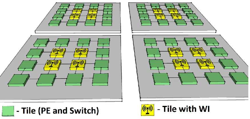
The primary aim of the proposed architecture is to seamlessly unify inter and
intrachip networks such that data can be transmitted between cores on a single chip as well
as between cores on multiple chips in a system. This architecture is a hybrid network with
both wired and wireless interconnects. Every core in the multichip system is integrated
with a NoC switch, and the switches within each independent chip are interconnected using
[image:23.612.93.530.308.517.2]an intrachip NoC architecture.
Fig. 3: Architecture of the proposed wireless multichip system
Wireless Interfaces (WIs) are integrated in a select few switches in the each of these
chips in order to realize interchip wireless communication. To be equipped with the WIs,
the internal cores are efficiently selected such that, on an average, every other core will be
14
counterparts in the same chip as well as other chips. Fig. 3 shows the architecture of the
proposed multichip system interconnected with inter and intrachip wireless network. This
figure is not to scale and is merely to provide an idea of how the architecture will be laid
out. The actual architecture however will involve much more cores on each of the chips,
and would be beyond the scope of a comprehensible diagram.
3.1.
Topology
Every core in the proposed multichip system is integrated with a NoC switch, and
the switches within each independent chip are interconnected using an intrachip NoC
architecture. The system is proposed with two different intrachip NoC topologies and their
interconnection architectures are described below:
3.1.1 Multichip System with Intrachip Mesh
The intrachip NoC topology employed here is a traditional mesh based NoC [4].
This topology consists of an m × n mesh of switches interconnecting the cores placed along
with those switches as shown in Fig.1. Every switch, except those at the edges, is connected
to four neighboring switches and one core, thus forming a mesh like orderly network
structure. Traditionally, for interchip communication, an I/O is connected to the periphery
of the chip onto one of the switches at the edge. This would mean that data packets from
the internal cores have to travel to the chip edge, get transmitted over the I/O onto the other
chip, and then get routed to its destination core. This multihop interchip communication
results in high latency and high energy consumption. As a solution, in this proposed
15
subnets and a switch at the center of each of these subnets is equipped with a Wireless
Interface (WI) for interchip data transfer. This logical placement of the WIs in the subnets
would avoid long multihop paths, and ensure that every core in the system can transmit
interchip data within just a few hops. This significantly improves the connectivity of the
entire multichip system by establishing direct wireless chip-to-chip links between internal
cores, thus eliminating the need to travel to and from the periphery of the chips.
3.1.2 Multichip System with Intrachip Small-World
While the NoC mesh topology is good, its performance is shown to improve by
inserting long-range shortcuts between distant cores using wired metal interconnects [28].
This new topology is called the Small-World network, which is a type of complex network,
often found in nature, characterized by both short-distance and long-range links. This
method reduces the average number of hops between nodes even for very large network
sizes, and thus improves the efficiency of the network. In order to further improve the
performance, these long-range metal interconnects are replaced by long-range wireless
links in [29]. Such a scalable topology is very well suited for designing a hybrid inter and
intrachip interconnection network using wireless links.
In order to establish the wireline links within each intrachip NoC while satisfying
the properties of small-world graphs, the wireline topology is generated according to the
inverse power law, to minimize wiring costs [30].
16
Where, P(i,j) is the probability of establishing a link between two switches i and j,
separated by a manhattan distance of lij. The distance is obtained by considering a
tile-based floorplan of the cores on the die. The frequency of communication between the
switches i and j is represented by fij and n is the total number of switches in the network.
This frequency of traffic interaction between the cores, fij, is also factored into (1) so that
more frequently communicating cores have a higher probability of having a direct link,
optimizing the topology for application-specific traffic. This frequency is expressed as the
percentage of traffic generated from i that is addressed to j and the frequency distribution
is based on the particular application mapped to the overall NoC and is hence known prior
to wireless link insertion. Therefore, a priori knowledge of the traffic pattern is used to
establish the topology with a correlation between traffic distribution across the NoC and
network configuration as in [31]. This optimizes the network architecture for non-uniform
traffic scenarios. The parameter α governs the nature of connectivity wherein a higher value
of α will result in lesser number of longer links. Hence, the value of α is chosen such that
[image:26.612.99.522.486.652.2]optimal wiring costs are obtained [30].
17
This power law based link distribution results in both short distance connections
and long-range links due to non-zero probability of links between far-away nodes. Fig.4
gives a diagrammatical representation of a typical small-world NoC. The link setup method
is repeated until every core or groups of cores are connected. As the links are established
probabilistically following (1) the number of ports of each switch may not be the same.
The average number of ports per switch is however constrained to be 5 to have the total
number of connections to be the same as that of the mesh based NoC. In the proposed
architecture with this small-world NoC, the same switches as in the mesh based system are
equipped with the WIs to reduce the path length of the interchip data accessing the WIs.
3.2.
Physical Layer
The proposed architecture is a hybrid network of both wired and wireless
interconnects. This multichip system will enable seamless intra and interchip
communications using wireless links. The on-chip communication will happen over the
hybrid wireline and wireless NoC, where the wireline links are realized with traditional
global-wire based interconnects depending on the topology adopted. As for the wireless
interconnections used for both intrachip and interchip communications, on-chip embedded
miniature antennas are used that can be fabricated within the chip to establish direct
chip-to-chip communication between internal cores. In this work, for the realization of these
wireless channels, on-chip metal zig-zag antennas are chosen. In [10], these antennas are
shown to be effective in establishing both on-chip and off-chip communication. It is also
shown in [10] that the metal mm-wave zig-zag antenna provides the best power gain for
18
fabricated using top layer metals and hence, are CMOS process compatible, making them
an excellent near-term solution to the wired interconnect problem. These mm-wave 60 GHz
antennas are shown to have a bandwidth of 16 GHz for both on-chip [9] and off-chip [24]
communications.
There is, however, one catch to the chosen antenna design. There is significant
variation in the antenna gain between on-chip and chip-to-chip communications. Hence, to
be able to support both intrachip and interchip communications, the adopted transceiver
needs to have a variable signal boosting capability. In [32], a Variable Gain Amplifier
(VGA) is proposed. This is shown to be suitable for variable length wireless interconnects
in [33], and hence is adopted in this proposed work. The adopted VGA module is proposed
to be utilized in two distinct gain settings, that is, the VGA based transceiver will use two
separate amplification paths with two different gains. At any instant of time, only one of
these paths will be active depending upon the chosen communication being on-chip or
chip-to-chip. The respective amplifier paths are activated by a simple control logic that is
based on the destination address determined at the network router or switch.
3.3.
Wireless Communication Protocol
The bandwidth of the wireless medium is limited by the transceiver design and the
on-chip antenna technology. To improve performance, multiple wireless transceivers
access the wireless medium and end up sharing a single frequency channel. This leads to
contention between the multiple transceivers and also interference. To alleviate this issue,
[9] showcases a token passing protocol where each of the WIs in a NoC architecture can
19
single transceiver can access the wireless medium at a time, which would be inefficient.
As a more efficient alternative, [21] shows a Direct Sequence Spread Spectrum (DSSS)
based Code Division Multiple Access (CDMA) scheme which enables multiple
simultaneous code-channels between multiple WIs in a system. Walsh codes are used to
create these code-channels in many CDMA application as they have a low spreading factor.
Spreading factor can be defined as the number of chips in a single codeword. As each bit
is encoded into one of these codewords, the effective data transfer rate decreases, that is,
the data transfer latency increases by the spreading factor. Hence, the Walsh codes with a
low spreading factor will have a lower impact on bandwidth of the individual
code-channels.
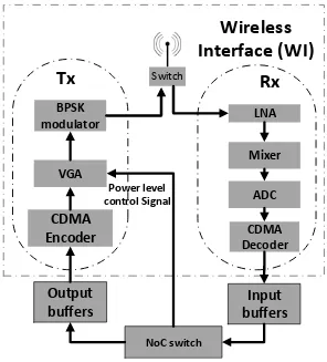
Output
buffers
Input
buffers
NoC switch
Wireless
Interface (WI)
Switch
BPSK modulator
CDMA
Encoder
VGA
Tx
LNA
Mixer
ADC
CDMA Decoder
Rx
[image:29.612.176.472.345.672.2]Power level control Signal
20
In this thesis, the CDMA based channel access mechanism is adopted, using Walsh
codes to create the orthogonal code-channels, thus enabling multiple access of the wireless
medium. Fig.5 depicts the mm-wave CDMA based wireless transceiver used in this thesis.
At the transmitter, the encoding is performed digitally by simply XOR-ing the bit and the
codeword, and the result is then amplified to the appropriate level by the VGA module
depending on the destination. This amplified signal is then modulated and mixed with the
carrier using a Binary Phase Shift Keying (BPSK) modulator. At the receiver, a
demodulator comprising of a Low Noise Amplifier (LNA) and a mixer is combined with a
low-power, high speed Analog to Digital Converter (ADC) and a CDMA decoder. The
orthogonal codes make sure that the correlation between different code-channels is zero
and that the bits transmitted in other channels do not affect the received bit. In this thesis,
a Transmitter-based CDMA protocol is adopted where each transmitter encodes the data
into specific code channels while the receivers are equipped with decoders for all the
channels. This means that, using these CDMA based wireless links, each receiver can
receive data from multiple transmitters concurrently but each transmitter can send data only
to a particular destination.
3.4.
Routing
The routing protocol for the proposed wireless multichip system is a seamless intra
and interchip data communication mechanism. Wormhole switching is adopted in this
work [5] for both inter and intrachip communication. Here, the data packets are broken
down into small units called flow control units or flits. The size of each flit is chosen such
21
multichip system have bidirectional ports for all links attached to it. The flits are routed
over the network using these switches, and each switch only forwards the first flit or the
header flit onto the next switch in the path to the destination. The rest of the flits (body
flits) follow this path setup by the header flit in a pipelined fashion. Hence each switch
only has local forwarding information, eliminating the need for maintaining non-scalable
global routing information. Virtual Channels (VCs) are used and each packet gets a distinct
virtual path to its destination. Hence, each switch can send and receive packets from
different nodes simultaneously.
As the overall system is not a regular network, a shortest path routing algorithm is
used to optimize network performance. A forwarding table based routing over
pre-computed shortest paths determined by Dijkstra’s algorithm is used. Owing to this, the
wireless links can also be used for intrachip communication if they reduce the path length
compared to a completely wireline path. This makes a significant contribution to the
routing mechanism of the proposed architecture. Deadlock is avoided by transferring flits
along the shortest path routing tree extracted by Dijkstra’s algorithm, as it is inherently free
22
Chapter 4
Simulation Results
This section gives an overview of the experimental setup of the proposed system
model, and evaluates its performance in detail. The wireless multichip architecture is a
hybrid network with both wired and wireless interconnects. The system is considered to
have 64 cores per chip, and the number of chips in the system is varied from one to a
maximum of four for this work’s experiments, yielding different systems of sizes 64, 128,
192 and 256 cores. Every core in the multichip system is integrated with a NoC switch,
and the switches within each independent chip are interconnected using an intrachip NoC
architecture using two different topologies as explained in Chapter 3. Wireless Interfaces
(WIs) are integrated in exactly 4 switches in the each of these chips in order to realize
interchip wireless communication. The on-chip zig-zag antennas considered in this work
for these WIs are able to provide a bandwidth of 16 GHz around a center frequency of 60
GHz [24]. The CDMA based wireless transceivers achieve a total data rate of 6 Gbps [21]
for all channels. The total power dissipation of this transceiver, which is the combined
power consumption of all its components including the CDMA encoder/decoder, BPSK
modulator, LNA mixer, ADC [21] and the VGA [32], is 20.6272 mW.
This proposed wireless multichip system is then compared with an equivalent
wireline I/O system. This wireline system also contains the same number of cores per chip
as the wireless multichip system, with the only difference being the interchip
interconnection, which is considered to be a high speed serial I/O [23]. The chip I/O is
connected to the periphery of the chip in one of the corner switches, irrespective of the
23
switch based architecture instead of a shared bus in order to enable concurrent
communication between the chips. The bandwidth of this I/O is 15 Gbps and its energy
consumption is 5 pJ/bit, i.e. a power dissipation of 75 mW at 15Gbps [23].
4.1.
Simulator Setup
In the experiments, a cycle accurate simulator is used in which the proposed
architecture is implemented and the progress of flits over the switches and the links per
cycle are monitored. For the data packets, a packet size of 64 flits is considered, with
each flit containing 32 bits. The architecture of the switches used in the NoC is
considered with 3 stages, namely, input, output arbitrations and routing [4]. These
switches are considered to have 4 Virtual Channels (VCs) in each input and output ports,
irrespective of the NoC topology adopted. Each of these VCs has a buffer depth of 2 flits
except for the switches incorporated with the WIs, which have an increased buffer depth
of 32 flits. This is done so that the CDMA transceivers can accommodate simultaneous
reception from multiple sources.
The performance of the system is evaluated for both uniform random traffic and
non-uniform traffic. Every simulation is run for ten thousand clock cycles allowing for
transients to settle in the first few thousand cycles accounting for flits that are routed and
stalled. All the wired links in the mesh based NoC consume just one clock cycle for
transmitting a flit. However, in the small-world NoC, some on-chip wireline links take up
more than one clock cycle for flit transmission, and hence, are pipelined by inserting
FIFO buffers such that, between by two stages, it is possible to transfer an entire flit in a
24
The simulator is annotated with the power consumption parameters of both the wireless
links and the serial I/O interconnections (as explained above in section 4) in order to
model the energy consumption of data exchange in the system. The energy dissipation,
area overheads and timing requirements of the NoC switches and the WIs are obtained
from post synthesis RTL design using 65 nm standard cell libraries (http://cmp.imag.fr)
using Synopsis™ tool suites. The energy dissipation of the on-chip wireline links are
obtained from Cadence layout tools considering their actual dimensions obtained from
assuming a tile-based floorplan of the NoC on a 20 mm × 20 mm die area for each chip.
4.2.
Wireless Link Budget Analysis
In order to determine the transmitted power that is required to achieve an acceptable
BER on the intra and interchip wireless CDMA links, a link budget analysis is presented
in this section. The transmitted power, Pt of the wireless channels is given (in dBm) using
the following equation.
Pt = SNR + PL + Nf (2)
Where, SNR is the signal to noise ratio at the receiver (in dB), PL is the path loss (in dB)
and Nf is the receiver noise floor (in dBm). Assuming perfect orthogonality in the CDMA
code channels, an SNR of 15 dB results in a BER of less than 10-15 for the BPSK modulated
scheme adopted in this thesis. A BER of 10-15 is comparable to wireline data transfer in
current technologies. Hence, in this link budget analysis, a required SNR of 15 dB is
considered. In [9], it is shown that the path loss, PL, in intrachip links using mm-wave
25
interchip distances (a few centimeters) to be -35 dB. The third factor, Nf, of the receiver is
given by,
Nf = 10 log kTB + NF (3)
Where, k is the Boltzmann constant, T is the temperature, B is the bandwidth of the receiver
and NF is the noise figure of the receiver (in dB). This noise figure of the receiver depends
on the LNA and is given by,
𝑁𝐹 = 10 log(1 + 𝐹𝐿𝑁𝐴+
𝐹𝑚𝑖𝑥𝑒𝑟
𝐺𝐿𝑁𝐴 ) (4)
Where, FLNA, Fmixer and GLNA are the noise figure, mixer and the gain of the LNA
respectively. In [21], the value of NF is given to be 6.3 dB. This makes the receiver noise
floor -69.43 dBm at 50 degrees C. Consequently, the output of the transmitter is -28.93
dBm and -19.43 dBm for intra and interchip links respectively. The two different
transmitted powers are generated by using the VGA module discussed in section 3.2. The
power consumption of the transceivers including the VGA module is considered in the
following sections for performance evaluation.
4.3.
Performance Evaluation
There are two metrics being considered for performance evaluation of the multichip
system: maximum achievable bandwidth per core and packet energy dissipation.
The maximum achievable bandwidth per core is given as the peak sustainable data
rate in number of bits successfully routed per core per second at network saturation. This
is given as B,
26
Where, t is the maximum throughput in number of flits received per core per clock cycle
at network saturation, β is the number of bits in a flit, and f is the clock frequency. The
throughput is directly obtained from system level simulations performed by the cycle
accurate simulator described in section 4.1.
The average packet energy dissipation is defined as the average energy dissipated in
transmission of a packet from source to destination. It is given by adding the energy
dissipation of all the components in the multichip system (buffers, switches, links, etc.) and
dividing this sum by the total number of packets that were successfully routed. This total
sum will always include the energy dissipation of the WIs as they are always active in the
wireless multichip system. However, for the wireline multichip system, the energy
dissipated by the I/O is added to the sum only when a flit traverses the I/O.
In the following subsections, the performance of the proposed wireless multichip
system is evaluated based on the above mentioned metrics. Furthermore, this performance
is compared with that of the wireline I/O based multichip system. This comparison involves
four different interconnect architectures in total due to the consideration of two different
topologies for each multichip system.
i. Mesh + I/O: In this architecture, the intrachip communication occurs through the
mesh based NoC and the interchip communication happens through the serial I/O,
where the I/O is connected to a single corner switch of every chip. This architecture
is completely wireline.
ii. Small-World + I/O: Here, the intrachip communication occurs through the
small-world based NoC topology and the interchip communication happens through the
27
iii. Mesh + CDMA: In this architecture, the intrachip communication happens over
both the conventional wireline mesh links as well as the wireless links, while the
interchip communication only uses the wireless links connecting WIs in different
chips.
iv. Small-World + CDMA: Here, the intrachip communication uses the wireline
small-world based NoC as well as the wireless interconnections, whereas only the
wireless chip-to-chip links are utilized for interchip communication.
The four different architectures are summarized in Table 1 for convenience.
Table 1: Different interconnection architectures for multichip system
Architecture Mesh based NoC Small-World NoC Involves Wireless Links Serial I/O module Wireless Interchip links
Mesh + I/O Small-World + I/O Mesh + CDMA Small-World + CDMA
Intrachip Communication Interchip Communication
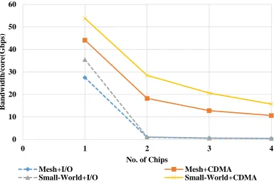
4.3.1 Achievable Bandwidth
In this section, the peak achievable bandwidth per core of the multichip system is
evaluated at network saturation using uniform random traffic. As mentioned earlier, the
each chip in the multichip system is considered to contain 64 cores, and the number of
chips is varied from one to a maximum of four chips, yielding four different system sizes
of 64, 128, 192 and 256 cores. The four different interconnect architectures listed in section
28
are considered per chip. In Fig. 6 the peak achievable bandwidth per core is shown for the
[image:38.612.122.507.137.396.2]multichip system.
Fig. 6: Peak achievable bandwidth per core for varying system size, for uniform traffic
From the figure, it can be observed that both the architectures with wireless CDMA
interconnects have higher bandwidth compared to the wireline I/O interconnections. As the
system size is increased, the bandwidth of the wireless system decreases, but not as
significantly as the wireline system. In other words, the wireless CDMA architectures have
higher bandwidths for all system sizes. This is due to the fact that the data in the wireline
multichip system needs to travel from the internal cores to the periphery of the chip (to the
corner switch with I/O), get routed over the I/O to the destination chip, and then travel to
the destination core in that chip. This multihop transmission of data is avoided in the 0
10 20 30 40 50 60
0 1 2 3 4
B
and
w
idt
h/c
ore
(G
bp
s)
No. of Chips
Mesh+I/O Mesh+CDMA
29
wireless architectures where the WIs provide direct chip-to-chip connectivity between
internal cores using the single-hop interchip wireless links. The performance of the wireline
system is further degraded due to congestion at the I/O module since it is connected to only
one switch of a chip. Furthermore, the wireless bandwidth is distributed among multiple
CDMA links. While the bandwidth of each link reduces due to the spread spectrum CDMA
technique, the simultaneous multiple access by multiple transmitters contribute to an
improvement in performance. Therefore, even though the aggregate wireless channel
bandwidth of 6 Gbps is less than the I/O bandwidth of 15 Gbps, the overall performance is
much better than the wireline multichip system. This also means that the wireless system
is much more scalable than its wired counterpart.
When comparing across topologies, it can be seen that the small-world NoC
performs better than the mesh based NoC for both the wireline and the wireless systems.
This is due to the direct one-hop connections between distant cores on the chip available
on the small-world NoC, thus reducing multihop communications significantly. Also, the
performance gain is more significant in the single chip system because as the number of
chips increases, the impact that the local NoC have on the overall system decreases, which
in turn results in the decrease of overall system performance.
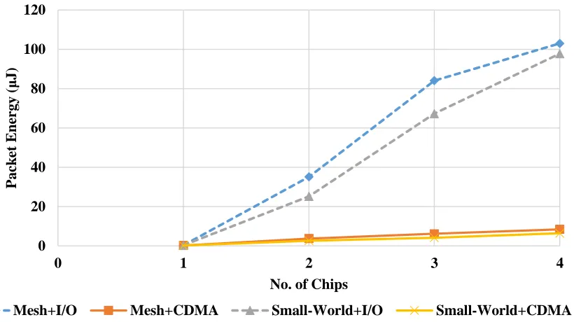
4.3.2 Packet Energy
The packet energy dissipation of the multichip system is evaluated in this section
and compared between the different interconnect architectures. Fig.7 shows the packet
30
Fig. 7: Average packet energy dissipation with varying system size, with uniform traffic
It can be observed from the figure that the packet energy increases significantly for
the I/O based architectures when the system size is scaled up, while that of the wireless
architectures do not increase drastically. This is due to the same fact, as described in the
previous section, that the wireline system involves multihop interchip communication.
Also, the I/O module is connected to only a single corner switch in each chip, and so, is
prone to congestion at this switch. As the number of chips increases, the percentage of
interchip traffic also increases which implies that a much larger number of packets need to
use the interchip I/O interconnections. This creates a bottleneck at the I/O modules and
causes a drastic decrease in bandwidth per core and hence an increase in the buffering
energy at those modules. Furthermore, this I/O interconnection is considered to be a switch
based architecture instead of a shared bus in order to enable concurrent communication 0
20 40 60 80 100 120
0 1 2 3 4
P
ack
et
E
n
ergy
(μ
J
)
No. of Chips
31
between the chips. This leads to the interchip communication dissipating high energy due
to the intermediate I/O switches in the path of the interchip data. This results in the sharp
increase in packet energy dissipation with increase in the number of chips.
One more important observation is that the gain in the energy efficiency of the
wireless systems increases over the wireline system increases with increase in the number
of chips. This is because the interchip traffic increases with increase in the number of chips,
causing congestion problems in the wireline system. However, the wireless links being
distributed among the cores in the chips alleviates this problem and hence, is much more
energy efficient with increase in system size. Comparing across topologies, it is seen that
the small-world based NoC have lower packet energy than its mesh based counterparts.
This is again due to the single-hop long range links on the chips in the small-world
architecture. However, as discussed in the previous section, this gain diminishes as the
system size increases due to the diminishing impact of the individual NoCs on the overall
system performance.
4.4.
Performance Evaluation with Non-Uniform Traffic
Having established the performance of the wireless multichip system under uniform
random traffic, this section analyzes the performance of the system with non-uniform
traffic patterns. In this case, only the small-world based architectures are considered for
evaluation and comparison with each other, namely, the World + I/O and the
Small-World + CDMA architectures. The traffic patterns considered are hotspot traffic and an
application specific traffic from a FFT based workload. In hotspot traffic, 5% of all the
32
which is called the hotspot. The rest of the packets are distributed equally among all other
cores. As for the FFT traffic, a 256-point Fast Fourier Transform (FFT) application was
considered, wherein each core performs a 2-point radix-2 FFT computation.
Fig. 8(a): Peak achievable bandwidth per core with non-uniform traffic
Fig. 8(b): Packet Energy with non-uniform traffic
0 10 20 30 40 50 60
1 Chip 2 Chips 1 Chip 2 Chips
HotSpot Traffic FFT Traffic
B andw idth /C or e( G bps) Small-world+I/O Small-world+CDMA 0 3 6 9 12 15 18 21 24 27 30 33
1 Chip 2 Chips 1 Chip 2 Chips
HotSpot Traffic FFT Traffic
[image:42.612.127.511.166.364.2] [image:42.612.143.518.429.640.2]33
Fig.8(a) and Fig.8(b) represent the bandwidth and the packet energy for the
small-world NoC based multichip system with the above two traffic patterns, at network
saturation. It can be observed from these figures that the wireless small-world architecture
outperforms the I/O based multichip system for the two non-uniform traffic patterns. In
case of hotspot traffic, the interchip data transfer is substantially high since all the cores
from all the chips send a certain percentage of the packets to one particular destination.
This results in serious congestion at the I/O modules and hence degrades the performance
significantly. This issue is mitigated in the wireless architecture due to the distributed
wireless links in each chip. As for the FFT traffic, the pattern is more distributed and so,
though there exists some degradation in bandwidth and energy efficiency, it is not as
significant as that of hotspot traffic. These results showcase that the wireless interchip
interconnection architecture can be beneficial for a variety of applications mapped into
such multichip multicore systems.
From these observations, it can be concluded that there exists a strong correlation
between the performance of the multichip system and the proportion of the interchip traffic.
This is further analyzed by evaluating the performance of the system while varying the
degree of localization in the traffic. The localization parameter is defined as the percentage
of data packets from each core that has a destination within the same chip. This parameter
is varied from 25% to 100% for a 2 chip system for two different architectures, namely,
the Small-World + I/O and the Small-World + CDMA. Fig.9(a) shows the variation of
bandwidth per core and Fig.9(b) shows the variation of packet energy, with changing
34
Fig. 9(a): Peak Bandwidth per core for 2 chip system with localization
Fig. 9(b): Average packet energy for 2 chip system with localization
These figures represent how the peak bandwidth per core and the average packet
energy vary with different possible traffic patterns. It can be observed that as the
localization parameter increases the bandwidth of the multichip systems increases and the 0 10 20 30 40 50 60
25 50 75 100
B andw idth / C ore (G bps) Localization % Small-world+I/O Small-world+CDMA 0 50 100 150 200 250 300
25 50 75 100
[image:44.612.147.509.77.270.2] [image:44.612.130.514.342.562.2]35
packet energy consumption decreases. For low localization percentage, a higher amount of
traffic accesses the interchip interconnections and the gains of the wireless links over the
wired I/O is high.
4.5.
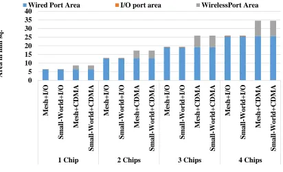
Area Overheads
The comparative area overheads of various architectures used in this thesis is
analyzed in this section. The number of wired intrachip links in all configurations are same
as that of a conventional mesh NoC. This is because the number of intrachip links in the
small-world + I/O and small-world + CDMA is constrained to be the same as that of the
conventional mesh. The only difference is the I/O module, the wireless transceivers and
the area of ports associated with them. Fig.10 depicts the total area overhead of the various
interconnection architectures for different multichip configurations and sizes considered in
[image:45.612.108.520.427.678.2]this work.
Fig. 10: Area overheads 0 5 10 15 20 25 30 35 40 Me sh+ I/ O Sma ll -Wo rl d+I /O Me sh+ C D MA Sma ll -Wo rl d+C D MA Me sh+ I/ O Sma ll -Wo rl d+I /O Me sh+ C D MA Sma ll -Wo rl d+C D MA Me sh+ I/ O Sma ll -Wo rl d+I /O Me sh+ C D MA Sma ll -Wo rl d+C D MA Me sh+ I/ O Sma ll -Wo rl d+I /O Me sh+ C D MA Sma ll -Wo rl d+C D MA
1 Chip 2 Chips 3 Chips 4 Chips
A rea in m m sq.
36
For the CDMA based wireless architectures, the transceiver which includes the ADC, the
modulator/demodulator and the CDMA codec, occupies an area of 0.4mm2 [21] whereas
the I/O based architectures has a transceiver area of 0.088mm2 [23]. For the wireless
multichip system of the largest configuration, the total area of the interconnection network
37
Chapter 5
Conclusions and Future Work
Computing modules in typical data center nodes or server racks consist of several
multicore chips on a board or a System-in-Package (SiP). The energy efficiency and data
bandwidth of such a multichip system is severely restricted by I/O based interchip
interconnections. This thesis explores the advantage of using state-of-the-art mm-wave
wireless links, operating in the 60 GHz band, for interconnecting such multichip systems.
The wireless links are proposed in order to alleviate the drawbacks of the multihop
communication while using serial I/O based interconnections. The wireless links also
successfully provide a seamless interconnection between on-chip and off-chip data
transfer, as opposed to the traditional method of decoupling them to facilitate design
flexibility. This thesis proposes the design of a seamless hybrid wired and wireless
interconnection network for multichip systems in a package, with dimensions spanning up
to tens of centimeters using on-chip wireless transceivers.. Even though the bandwidth of
such wireless links is not necessarily higher than the high speed serial I/O links, the wireless
links are used for seamless data transfer between cores on the same chip to augment
intrachip communication, as well as provide direct communication between cores on
different chips. Due to this multiple access of the wireless medium by multiple transceivers,
there are significant performance and energy efficiency gains on the overall system. It is
demonstrated with cycle accurate simulations that the proposed wireless multichip
architecture increases the bandwidth and reduces the energy consumption when compared
38
The architecture is also proven to scale significantly well with increase in system
size when compared to its wireline counterpart. Hence, in the future, this work can be
extended to be applicable to larger computing infrastructures consisting of several
multichip modules. While the scope of this thesis only encompasses smaller multichip
modules with distances up to tens of centimeters, the ideology can be extended to several
meters or more in the future, to be used in much larger infrastructures like servers or entire
39
Bibliography
[1] M.A. Horowitz et al., “The Future of Wires,” Proc. IEEE, vol. 89, no. 4, pp. 490-504, Apr. 2001
[2] C. Hsieh and M. Pedram, “Architectural Energy Optimization by Bus Splitting,” IEEE Tran. Computer-Aided Design, vol. 21, no. 4, pp. 408-414, Apr. 2002. 41 [3] Dally, W.J.; Towles, B., "Route packets, not wires: on-chip interconnection networks," Proceedings of Design Automation Conference, 2001. pp.684 – 689. [4] Pande, P.P.; Grecu, C.; Jones, M.; Ivanov, A.; Saleh, R., "Performance evaluation and design trade-offs for network-on-chip interconnect architectures," Computers, IEEE Transactions on , vol.54, no.8, pp.1025,1040, Aug. 2005
[5] Duato, J.; Yalamanchili, S. and Ni, L.; 2002. Interconnection Networks-An Engineering Approach. Morgan Kaufmann, (2002).
[6] PCI-SIG, “PCI Express Architecture,” URL: http://www.pcisig.com.
[7] Xiaowen Wu; Yaoyao Ye; Wei Zhang; Weichen Liu; Nikdast, M.; Xuan Wang; Jiang Xu, "UNION: A unified inter/intra-chip optical network for chip multiprocessors," 2010 IEEE/ACM International Symposium on Nanoscale Architectures (NANOARCH), pp.35,40, 17-18 June 2010.
[8] Topol, A.W.; Tulipe, D.C.La; Shi, L.; Frank, D.J.; Bernstein, K.; Steen, S.E.; Kumar, A.; Singco, G.U.; Young, A.M.; Guarini, K.W.; Ieong, M. 2006. Three-dimensional integrated circuits. IBM Journal of Research and Development , vol.50, no.4.5, pp.491,506, July 2006.
[9] Chang, K.; Deb, S.; Ganguly, A.; Yu, X.; Sah, S. P.; Pande, P. P.; Belzer, B. and Heo, D. 2012. Performance evaluation and design trade-offs for wireless network-on-chip architectures. J. Emerg. Technol. Comput. Syst. (Aug. 2012), 23:1–23:25.
[10] Lin, J.; Wu, H-T.; Su, Y.; Gao, L.; Sugavanam, A.; Brewer, J.E.; O, K.K. 2007. Communication Using Antennas Fabricated in Silicon Integrated Circuits. IEEE
Journal of Solid-State Circuits, (Aug. 2007), 1678-1687.
40
Using 43-GHz Transceivers and Bond-Wire Antennas," Solid-State Circuits, IEEE Journal of , vol.44, no.10, pp.2711,2721, Oct. 2009.
[12] International Technology Roadmap for Semiconductors, 2012 Edition, URL: http://www.itrs.net/.
[13] C. Hsieh and M. Pedram, “Architectural Energy Optimization by Bus Splitting,” IEEE Trans. Computer-Aided Design, vol. 21, no. 4,pp. 408-414, Apr. 2002.
[14] P. Guerrier and A. Greiner, “A Generic Architecture for On-Chip Packet-Switched Interconnections,” Proc. Design and Test in Europe (DATE), pp. 250-256, Mar. 2000. [15] S. Kumar et al., “A Network on Chip Architecture and Design Methodology,” Proc. Int’l Symp. VLSI (ISVLSI), pp. 117-124, 2002.
[16] F. Karim et al., “An Interconnect Architecture for Networking Systems on Chips,” IEEE Micro, vol. 22, no. 5, pp. 36-45, Sept./Oct. 2002.
[17] P.P. Pande, C. Grecu, A. Ivanov, and R. Saleh, “Design of a Switch for Network on Chip Applications,” Proc. Int’l Symp. Circuits and Systems (ISCAS), vol. 5, pp. 217-220, May 2003.
[18] Deb, S.; Ganguly, A,; Pande, P. P.; Belzer, B.; and Heo, D. 2012. Wireless NoC as Interconnection Backbone for Multicore Chips: Promises and Challenges. IEEE Journal on Emerging and Selected Topics in Circuits and Systems, vol. 2, no. 2, (2012)
228–239.
[19] Abadal, S.; Alarcón, E.; Cabellos-Aparicio, A.; Lemme, M.; Nemirovsky, M. 2013, Graphene-enabled wireless communication for massive multicore
[20] Ganguly, A.; Chang, K.; Deb, S.; Pande, P. P.; Belzer, B.; and Teuscher, C. 2011. Scalable Hybrid Wireless Network-on-Chip Architectures for Multicore Systems. IEEE Transactions on Computers, 60, 10, (2011), 1485–1502.
[21] Vijayakumaran, V.; Yuvaraj, M. P.; Mansoor, N.; Nerurkar, N.; Ganguly, A. and Kwasinski, A. 2014. CDMA Enabled Wireless Network-on-Chip. J. Emerg. Technol. Comput. Syst. 10, 4, Article 28 (June 2014), 20 pages.
41
Electronic Packaging and Systems (EPEPS), 2010 IEEE 19th Conference on, 1,4, (Oct.
2010), 25-27.
[23] G. Balamurugan, J. Kennedy, G. Banerjee, J. E. Jaussi, M. Mansuri, F. O’Mahony,
B. Casper, and R. Mooney, “A scalable 5-15 Gbps, 14–75 mW low-power I/O transceiver in 65 nm CMOS,” IEEE J. Solid-State Circuits, vol. 43, no. 4, May 2008.
[24] Yeh, H-H.; Melde, K.L. 2012. 60 GHz multi-antenna design in Multi-Core system. Antennas and Propagation Society International Symposium (APSURSI), 2012 IEEE , 1,2, (July 2012), 8-14.
[25] Chandran, U.; Zhao, D. 2014. Cost-optimal design of wireless pre-bonding test framework. System-on-Chip Conference (SOCC), 27th IEEE International, (2-5 Sept. 2014) 324-329.
[26] Laha, S.; Kaya, S.; Matolak, D.W.; Rayess, W.; DiTomaso, D.; Kodi, A. 2015. A New Frontier in Ultralow Power Wireless Links: Network-on-Chip and Chip-to-Chip Interconnects. Computer-Aided Design of Integrated Circuits and Systems, IEEE Trans. on, 34, 2, (Feb. 2015), 186-198.
[27] Shin, J-Y.; Sirer, E. G.; Weatherspoon, H. and Kirovski, D. 2012. On the feasibility of completely wireless datacenters. In Proceedings of the eighth ACM/IEEE symposium on Architectures for networking and communications systems (ANCS '12).
ACM, (New York, USA), 3-14.
[28] Ogras, U.Y.; Marculescu, R., 2006. It's a small world after all: NoC performance optimization via long-range link insertion. IEEE Transactions on Very Large Scale Integration (VLSI) Systems, (July 2006), 693-706.
[29] Ganguly, A.; Wettin, P.; Chang, K.; and Pande, P. P. 2001. Complex network inspired fault-tolerant NoC architectures with wireless links. In 2011 Fifth IEEE/ACM International Symposium on Networks on Chip (NoCS), (2011), 169–176.
42
[31] P. Bogdan and Radu Marculescu, “Quantum-Like Effects in Network-on-Chip Buffers Behavior,” Proc. of IEEE Design Automation Conference, DAC, 4-8 June, 2007, pp. 266-267.
[32] Daly, D.; and Chandrakasan, A. 2007. An energy-efficient ook transceiver for wireless sensor networks. Solid-State Circuits, IEEE Journal of, vol. 42, no. 5, (2007), 1003–1011.
[33] Mineo, A.; Palesi, M.; Ascia, G.; Catania, V. 2014. An adaptive transmitting power technique for energy efficient mm-wave wireless NoCs. Design, Automation and Test in Europe Conference and Exhibition (DATE), (March 2014), 24-28.
[34] Favi, C.; Charbon, E., "Techn
![Fig. 4: Small-World NoC architecture with short and long range links [29]](https://thumb-us.123doks.com/thumbv2/123dok_us/41691.3532/26.612.99.522.486.652/fig-small-world-noc-architecture-short-range-links.webp)