International Journal of Innovative Technology and Exploring Engineering (IJITEE) ISSN: 2278-3075, Volume-8, Issue- 6S4, April 2019
Abstract—The decoders are widely used in the logical circuits, data transfer circuits and analog to digital conversions. A mixed logic design methods for the line decoders are used to combining the transmission gate logic, pass transistor logic, and complementary metal-oxide semiconductor (CMOS) technology provides desired operation and performance. A novel topology is presented for the 2 to 4 decoder requires a fourteen transistor topology aiming on reducing the transistor count and operating power and a fifteen transistor topology aiming on high power and low delay performance. The standard and inverting decoders are designed in each of the case, gives a total of four new designs circuits. All the proposed decoders have compact transistor count compared to their conservative CMOS technologies. Finally, a variety of proposed designs present a noteworthy improvement in operating power and propagation delay, outperforming CMOS in almost all the cases.
Keywords—Decoders, Mixed Logic design , Power and Delay Optimization
I. INTRODUCTION
General decoders occupy more space in internal circuits. A general conventional 2-4 decoder can be designed using two inverters and four AND gates which totally comprises of 28 transistors. Similarly, a 4-16 conventional decoder can be designed using 4 inverters and 16 AND gates, totally of 104 transistors. These sizes can be reduced using new mixed logic which uses Pass Transistor Logic and Transmission Gate Logic. Pass transistor Logic also improves speed and power. The CMOS circuits are having more Propagation Delay, Power Dissipation and they occupy more Area on the Die. The proposed technology will reduce all these parameters as less as possible.
The CMOS technology is widely used in the Integrated Circuit design which includes starting from basic digital logic gates to a System on Chip (SoC)[2]. The complementary metal oxide semiconductor (CMOS) technology uses both n-channel enhancement mode metal oxide semiconductor field effect transistor (MOSFET) and p-channel enhancement mode MOSFET also NMOS transistor used as pull down network and PMOS transistor is used as pullup network to achieve the better in and fan-out capabilities. The CMOS logic circuits withstand against the different voltage scaling, it allows transistor channel sizing to a nanotechnology so that this technology can achieve high speed of operation as well as low power
Revised Manuscript Received on April 12, 2019.
Chandra SekharSavalam, Department of ECE, Dhanekula Institute of Engineering and Technology, Vijayawada.A.P, India.
KorapatiPrasanti, Department of EIE, VR Siddhartha Engineering College, Vijayawada.A.P, India.
A.S.Haranath, Department of ECE, Dhanekula Institute of
dissipation [3]. The pass transistor logic (PTL) was introduced in early 90’s and different design methods are presented [4] to [6], targeting to generate other possibilities to achieve the high speed and occupies less area on the die by applying the inputs directly to the gates of the Transistors and drain –source terminals of the MOSFET. The transmission gate logic designs used either NMOS or PMOS transistors that are connected parallel pairs where as the pass transistor designs uses individual PMOS and NMOS transistors. The Decoders are widely used in the all digital circuits, input and output circuits, data transmission modules, memory devices and all fundamental digital circuits.
II. DESIGN OF MIXED LOGIC CIRCUITS
A. Conventional Design
[image:1.595.361.494.481.555.2]The fundamental digital module is the decoder which decodes the coded input which is generally used in the all types of memory devices.Most common decoder circuit is an n input to 2n outputbinary decoder. In the conventional design the CMOS technology is used to design the logic of any application.
Fig.1.Block diagram of 2-4 Decoder.
Fig. 2. 2-4 decoder Gate level diagram.
Design and Implementation of High
Performance and Low Power Mixed Logic
Line Decoders
H L H H L H
H H H H H L
B. Pass Transistor Logic
[image:2.595.47.290.50.241.2]The Pass transistor logic uses more NMOS and PMOS transistors which are used in parallel or series to make the desired logic. In this PTL logic the transistors act as switches to propagate the VDD to the output port so that the desired logic is achieved.This method reduces the total number of the active transistors but it has a drawback of the voltage variation is present at the output of each stage it propagating to the final output stage. So this PTL design methods are exclusively for the some specific applications rather than the regular designs.
Fig. 3.Logic AND as well as OR Gates Circuits(3-transistor). (a) Transmission Gate Logic AND gate. (b) Transmission Gate Logic OR gate. (c) Dual Value Logic
AND gate. (d) Dual Value Logic OR gate.
The above fig.3 (a) shows a transmission gate logic AND gate which operates when both X and Y are logic High [H,H] then only the output gives the logic high value otherwise the output is logic zero value. Similarly fig 3. (b) shows the OR gate which operate when either X or Y are at logic high then the output logic high otherwise the output is logic zero. Both the cases the circuits require only one transmission gate and one NMOS transistor. Fig 3.(c),(d) shows dual value logics of the AND gate and OR gate which are required only 3-transistors when compared to conventional CMOS 6-transistors design.
C. Transmission Gate Logic
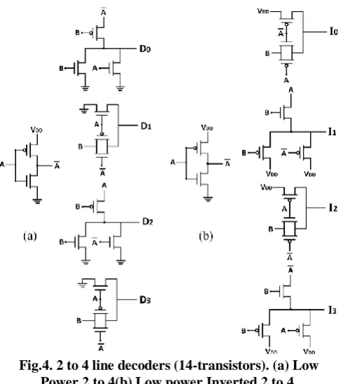
The transmission gate logic has the advantage of maintaining the good output voltage value over the pass transistor logic that is why transmission gates are widely used. In the proposed design uses the transmission gate logic
[image:2.595.306.551.211.485.2]decoders.
Fig.4. 2 to 4 line decoders (14-transistors). (a) Low Power 2 to 4(b) Low power Inverted 2 to 4.
[image:2.595.51.291.379.507.2]International Journal of Innovative Technology and Exploring Engineering (IJITEE) ISSN: 2278-3075, Volume-8, Issue- 6S4, April 2019
Fig.5. 2 to 4 line decoders (15-transistors). (a) High Power 2 to 4(b) High power Inverted 2 to 4.
III. IMPLEMENTATION OF DECODERS USING MIXED LOGIC
Mixed logic 2-4 line decoders are designed using the Mentor Graphics EDA Tools which is Pyxis Schematic editor to draw the Low power , Low power Inverting , High Power and High Power Inverting decoders. After designing these circuits we need to check the circuit checking to avoid the electrical errors and unwanted shorts while making the contacts.
Fig.6.2-4 Decoder LP (14 Transistors) circuit.
Fig.7.2-4 Decoder LPI (14 Transistors) circuit
Fig.8.2-4 Decoder HP (15 Transistors) circuit
circuits. The netlist also generated for the each decoder circuit successfully and the Power, Area, and propagation Delay are calculated for each of the circuit.
Fig.10. 2-4 Decoder LP Layout Diagram.
Fig.11. 2-4 Decoder LPI Layout Diagram.
Fig.12. 2-4 Decoder HP Layout Diagram.
Fig.13. 2-4 Decoder HPI Layout Diagram.
International Journal of Innovative Technology and Exploring Engineering (IJITEE) ISSN: 2278-3075, Volume-8, Issue- 6S4, April 2019
Fig.14. 4-16 Decoder HP circuit.
Fig.15. 4-16 Decoder HP Layout Diagram.
The above Fig.14 shows a 4-16 High performance decoder circuit and Fig.15 shows the Layout diagram for the 4-16 High performance decoders.
IV. RESULTS
The simulation is done for all the 2-4 LP, 2-4 LPI, 2-4 HP, 2-4 HPI and 4-16 HP decoders by using the AMS ELDO Simulator from the Mentor Graphics EDA which uses the CMOS 130nm Technology for the NMOS and PMOS transistors to making mixed logic designs. The below Fig.16, Fig.17, Fig.18, and Fig.19 are shows the simulation results for all transitions.
Fig.16. Input and output waveforms of Low power 2 to 4 decoder.
Fig.17. Input and output waveforms of Low power inverted 2 to 4 decoder.
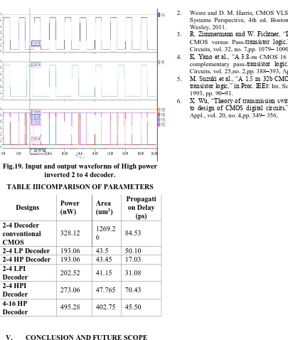
The pre-layout and post-layout simulations are done and analyzed for all the decoders before and after designing of the layout using the Mentor Graphics AMS ELDO simulation tool. The parameter comparison for all the mixed logic line decoders are listed on the Table.III which shows the great improvement on the performance, low power , high performance , low propagation delay and less area requirement when compared to the conventional CMOS designs.
Fig.19. Input and output waveforms of High power inverted 2 to 4 decoder.
TABLE IIICOMPARISON OF PARAMETERS
Designs Power (nW)
Area (um2)
Propagati on Delay
(ps) 2-4 Decoder
conventional CMOS
328.12 1269.2
6 84.53
2-4 LP Decoder 193.06 43.5 50.10 2-4 HP Decoder 193.06 43.45 17.03 2-4 LPI
Decoder 202.52 41.15 31.08
2-4 HPI
Decoder 273.06 47.765 70.43
4-16 HP
Decoder 495.28 402.75 45.50
V. CONCLUSION AND FUTURE SCOPE
The optimized parameters are like operating power and power dissipation, Area and Propagation delay of 2-4 decoder of both low power and high-performance circuits have calculated using Mentor Graphics Pyxis Schematic and Pyxis layout and CALIBRE Verification tool (DRC, LVS, PEX) for Physical Verification and Post Layout Simulation is done and for 4-16 decoders are designed the circuits and simulation is done using AMS ELDO. The Higher input /output Decoders can be extended to further by drawing Physical Layout and these Decoders can be used in Audio Frequency Applications like used at receiver end to decode the audio signal. It can also be used for memory address decoding. Generally, these decoders are frequently used in communication systems like telecommunications, networking and transfer of data from one end to another end.
REFERENCES
1. DimitriosBalobas and Nikos Konofaos, “Design of Low-Power HighPerformance 2-4 and 4-16 Mixed-Logic Line