EFFECT OF DIFFERENT PYROLYSIS AND ANNEALING
TEMPERATURE ON STRUCTURAL AND ELECTRICAL
PROPERTIES OF K
0.5Na
0.5(NbO)
3THIN FILM
DYANA ANAK CHAHIT
B051310115
EFFECT OF DIFFERENT PYROLYSIS AND ANNEALING
TEMPERATURE ON STRUCTURAL AND ELECTRICAL
PROPERTIES OF K
0.5Na
0.5(NbO)
3THIN FILM
This report is submitted in accordance with requirement of the University Teknikal Malaysia Melaka (UTeM) for Bachelor Degree of Manufacturing Engineering
(Engineering Materials) (Hons.)
by
DYANA ANAK CHAHIT B051310115
930722-13-5910
Disahkan oleh:
_____________________________ ______________________________ Alamat Tetap: Cop Rasmi:
29 PERUMAHAN BDA JALAN PENGIRAN MATHAIR 97000 BINTULU, SARAWAK
Tarikh: 22nd June 2017 Tarikh: _______________________
*Jika Laporan PSM ini SULIT atau TERHAD, sila lampirkan surat daripada pihak berkuasa/organisasi berkenaan dengan menyatakan sekali sebab dan tempoh laporan PSM ini perlu dikelaskan sebagai SULIT atau TERHAD.
UNIVERSITI TEKNIKAL MALAYSIA MELAKA
BORANG PENGESAHAN STATUS LAPORAN PROJEK SARJANA MUDA
Tajuk: EFFECT OF DIFFERENT PYROLYSIS AND ANNEALING
TEMPERATURE ON STRUCTURAL AND ELECTRICAL PROPERTIES OF K0.5Na0.5(NbO)3 THIN FILM
Sesi Pengajian: 2016/2017 Semester 2
Saya DYANA ANAK CHAHIT (930722-13-5910)
mengaku membenarkan Laporan Projek Sarjana Muda (PSM) ini disimpan di Perpustakaan Universiti Teknikal Malaysia Melaka (UTeM) dengan syarat-syarat kegunaan seperti berikut:
1. Laporan PSM adalah hak milik Universiti Teknikal Malaysia Melaka dan penulis. 2. Perpustakaan Universiti Teknikal Malaysia Melaka dibenarkan membuat salinan
untuk tujuan pengajian sahaja dengan izin penulis.
3. Perpustakaan dibenarkan membuat salinan laporan PSM ini sebagai bahan pertukaran antara institusi pengajian tinggi.
4. *Sila tandakan (√)
(Mengandungi maklumat yang berdarjah keselamatan atau kepentingan Malaysiasebagaimana yang termaktub dalam AKTA RAHSIA RASMI 1972)
(Mengandungi maklumat TERHAD yang telah ditentukan oleh organisasi/ badan di mana penyelidikan dijalankan)
SULIT
TERHAD
DECLARATION
It is hereby that all the materials in this thesis entitled “Effect of Different Pyrolysis and
Annealing Temperature on Structural and Electrical Properties of K0.5Na0.5 (NbO)3 Thin Film” are the result of my own work and all the materials that are not the result of my own had been clearly acknowledged in this thesis.
APPROVAL
This report is submitted to the Faculty of Manufacturing Engineering of UTeM as a partial fulfillment to the requirements for the Bachelor Degree of Manufacturing Engineering (Engineering Materials) (Hons). The member of the supervisory is as follows:
i
ABSTRAK
ii
ABSTRACT
iii
DEDICATION
iv
ACKNOWLEDGMENT
Praise to God, The Most Merciful, who has given me the strength, spirit and ability to complete successfully this work.
Special thanks to my supervisor, PM Dr. Mohd Warikh bin Abd Rashid for his guidance, support and patient throughout the development of this project.
I would also express my appreciation to my family, laboratory technicians and friends for helping and give support for me to complete this project with success.
v
TABLE OF CONTENTS
Abstrak i
Abstract ii
Dedication iii
Acknowledgement iv
Table of Content v
List of Tables viii
List of Figures ix
List of Abbreviations , Symbols And Nomenclature x
CHAPTER 1: INTRODUCTION
1.1 Background of Study 1
1.2 Problem Statement 2
1.3 Objective 3
1.4 Scope 3
CHAPTER 2: LITERATURE REVIEW
2.1 Introduction of Piezoelectric 5 2.1.1 Piezoelectric Ceramics 6 2.1.2 Lead Free Piezoelectric Material 8 2.1.3 Potassium Sodium Niobate (KNN) 9
2.2 Thin Film 11
2.2.1 Thin Film Application 11 2.3 Physical Deposition Techniques 12
2.3.1 Sputtering 12
vi
2.4.1 Atomic Layer Deposition (ALD) 14
2.4.2 Sol-gel 15
2.5 Processing Method 15
2.5.1 Spin Coating 15
2.6 Characterization of The Material 16 2.6.1 X-ray Diffraction (XRD) 16
2.6.2 Raman Spectroscopy 17
2.7 Morphology Analysis 18
2.7.1 Scanning Electron Microscopy (SEM) 18
2.8 Electrical Properties 19
2.8.1 Resistivity 19
2.9 Electrical Properties Testing 20 2.9.1 Four Point Resistivity Test 20
CHAPTER 3: METHODOLOGY 22
3.1 Introduction 22
3.2 Experimental Procedure Flowchart 23
3.3 Experimental Procedure 24
3.3.1 Raw Material 24
3.4 Sample Preparation 24
3.4.1 Sol-Gel Method 24
3.5 Substrate Preparation 25
3.5.1 Substrate Cutting 25
3.5.2 Ultrasonic Cleaning 26
3.6 Spin Coating Process 27
3.7 Pyrolysis 27
3.8 Annealing 28
3.9 Scanning Electron Microscopy 29
3.10 X-Ray Diffraction 29
3.11 Raman Spectroscopy 30
vii
CHAPTER 4: RESULTS & DISCUSSION 31
4.1 Introduction 31
4.2 X-Ray Diffraction 31
4.2.1 Pyrolysis Temperature 31
4.2.2 Annealing Temperature 33
4.3 Raman Spectroscopy 35
4.4 Scanning Electron Microscopy 37
4.5 Four Point Resistivity Test 40
CHAPTER 5: CONCLUSION AND RECOMMENDATION 41
5.1 Conclusion 41
5.2 Recommendation 42
REFERENCES 44
APPENDICES 49
A Gantt Chart of FYP I 50
viii
LIST OF TABLES
2.1 Properties of some selected lead free composition 10
3.1 Raw materials for the precursors 24 3.2 Weight percentages in sol-gel preparation 25
ix
LIST OF FIGURES
2.1 (a)Crystal structure of barium titanate above Curie temperature, (b)Crystal structure of barium titanate below Curie temperature
7
2.2 Phase diagram of PZT 8
2.3 Phase diagram of KNN 11
2.4 Sputtering deposition mechanism 13
2.5 Mechanism of spin coating 16
2.6 XRD pattern at different annealing temperature 17 2.7 RAMAN Spectra of KNN thin film 17 2.8 Electron and specimen interaction 18 2.9 SEM images OF KNN thin film at different annealing temperature 19 2.10 The polarization of electric field 19 2.11 Four point probe resistivity setup 21
3.1 (a) Silicon wafer cutting, (b) Silicon wafer substrate after cutting 26 3.2 POWERSONIC 410 Ultrasonic bath 26
3.3 TB-616 Spin coater 27
3.4 XMTD-702 Digital hotplate 28
3.5 OTF-1200X Thermal furnace 28
3.6 Four point probe I-V Keithley Probe 2400 source meter 30
4.1 XRD pattern for KNN thin film at different pyrolysis temperature 32 4.2 XRD pattern for KNN thin film at different annealing temperature 34 4.3 Raman spectra for KNN thin film based on different annealing
temperature 34
x
LIST OF ABBREVIATIONS, SYMBOLS AND
NOMENCLATURE
PZT - Lead zirconia titanate PbZrO3 - lead zirconate
PbTiO3 - lead titanate
˚C - Degree celcius
BT - barium titanate
MPB - morphotrophic phase boundary
BNT - bismuth sodium titanate
Tc - Curie temperature
WEEE - Waste Electrical and Electronic Equipment
KNN - potassium sodium niobate
RoHS - Hazardous Substances in electrical and electronic
equipment Si - Silicon
CH3COONa - Sodium acetate
CH3COOK - potassium acetate
Nb (OC2H5)5 - niobium penthaethoxide
CH3OCH2CH2OH - 2-metoxyethanol
XRD - X-ray diffraction
SEM - Scanning electron microscopy
BLSF - bismuth layer structured ferroelectrics pC/N - Pico per newton
Ec - coercive field
Pr - remnant polarization
xi
IC - Integrated Chip
Na - sodium K - potassium
PLD - Pulsed laser deposition
ALD - atomic layer deposition
CVD - chemical vapor deposition
ALE - atomic layer epitaxy
µm - micrometer
rpm - revolution per minute
MOCVD - metal organic vapor deposition
cm - centimeter
g/mol - gram per mol
g - gram
N2 - nitrogen
nm - nanometer
1
CHAPTER 1
INTRODUCTION
1.1Background of Study
Nowadays, the studies on piezoelectric materials have been extensively explored due to the rapid development of electronic industries. Piezoelectric materials are the materials that generate electricity due to the applied mechanical stress. Besides that, piezoelectric materials can work in reverse way such as if the electric current is applied, a strain will be generated. Due to the nature of piezoelectric materials itself, makes it is widely used in this electronic industries. The usage of piezoelectric ceramics have been widely used for sensors, actuators, transducers, buzzers and other electronic devices according to Du et al., (2006).
2
Therefore, in recent years, lead-free piezoelectric materials have been gained much attention. According to Panda & Sahoo, (2015), barium titanate (BT) is the first lead-free piezoelectric materials discovered during the World War II. In 1952, PZT was discovered and it is has better piezoelectric properties due to the occurrence of morphotrophic phase boundary makes it is an excellent candidates than BT. Other than that, Smolenski et al., (1960) has reported the existence of bismuth sodium titanate (BNT) but the sintering temperature of BNT is high about 1200 ˚C. In consequences, due to the volatility of bismuth, the high sintering temperature will results the loss of bismuth in the composition. According to Panda, (2009) ,even though BNT is the best option to replace PZT due to its high Curie temperature about 320˚C, but still it cannot replace PZT because of it has high coercive field and high electrical conductivity.
Until then, Saito et al., (2004) had developed a textured potassium sodium niobate (KNN) based ceramics and the properties are quite comparable to the unmodified PZT. KNN has high electrical properties, high Curie temperature (Tc) about 420˚C and friendly environment material. The idea of switching of PZT to KNN is supported by the Waste Electrical and Electronic Equipment (WEEE)’s law in 2006 and the usage of certain Hazardous Substances in electrical and electronic equipment (RoHS) is restricted due to protect the health and environment, Li & Wang (2012).
3 1.2Problem Statement
In recent years, the studies on potassium sodium niobate (KNN) have been gained much attention by researchers. It is because KNN is friendly environment material if compared to lead zirconia titanate (PZT) which has a large amount of lead which is a toxic substance and can cause damage to the kidney, brain, and nervous system as well as affect the children’s intelligence according to Du et al., (2006). Therefore, in electrical devices as well as the thin film application, the lead-free piezoelectric material such as KNN is the best choice to replace the PZT.
However, According to Haugen et al.,(2015), the fabrication of KNN by conventional solid state reaction technique is difficult due to the volatility of potassium (K) and sodium (Na) at higher calcination temperatures and duration which will results in the loss of potassium and sodium in the composition . In order to encounter the difficulties, according to Yan et al.,(2010) sol-gel method is introduced to synthesis KNN because of sol-gel method offers a low fabrication temperature.
In this study, KNN thin film is more preferable than KNN bulk ceramics. According to Yan et al.,(2010), memory, micro sensor and micro-actuator usually used ferroelectric and piezoelectric thin films compared to bulk ceramics. It is because, ferroelectric and piezoelectric thin films offer a lower operating voltage, easy to integrate with the Silicon (Si) technology and the cost is lower due to the less machining process according to Dausch et al., (2000).
4 1.3 Objective
The objectives of this project are:
i. To fabricate KNN thin film via sol-gel spin coating technique.
ii. To determine suitable pyrolysis and annealing temperature for fabrication of KNN thin film.
iii. To optimize the structural and ferroelectric properties of KNN thin film.
1.4 Scope
The scope of this study is to analyze the crystal structure, dielectric of KNN thin film by varying the pyrolysis and annealing temperature.
5
CHAPTER 2
LITERATURE REVIEW
2.1 Introduction of Piezoelectric
6
2.1.1 Piezoelectric ceramics
Piezoelectric ceramics are very hard, chemically inert and humidity or other atmospheric factor insensitive. Based on Kong and Wang (2003) ,the piezoelectric ceramic have the unstructured polarization. It is because the charge concentration of the unit cells are distinct from each other at a certain temperature range.
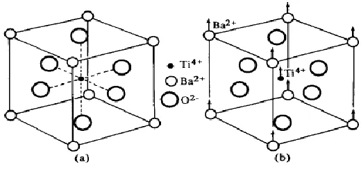
According to Yu (2014), Figure 2.1 (a) shows the crystal structure of the barium titanate above its Curie temperature. Its Curie temperature is about 120˚C. Above the Curie temperature, barium titanate appears to be in cubic crystal structure with Ba2+ ion at cube corner, O2- ions at the face center and Ti4+ at the body center. Meanwhile, Figure 2.1 (b) shows the crystal structure of barium titanate below its curie temperature and it is slightly deformed with Ba2+ and Ti4+ ions displaced relative to O2- ions. When it is slightly deformed, the material will exhibit the piezoelectric properties.
[image:22.612.180.440.430.552.2]
Figure 2.1 :(a) Crystal structure of barium titanate above Curie temperature, (b) Crystal structure of barium titanate below Curie temperature (Yu, 2014)
7
between lead zirconate (PbZrO3) which is known as PZ and lead titanate (PbTiO3) known as PT. According to,Panda & Sahoo,(2015), the rich compositions of zirconia (Zr) is in the rhombohedral state and the rich compositions of titanium (Ti) is in the tetragonal state and the morphotropic phase boundary of PZT is at the composition, x= 0.48 of PbTiO3. The permittivity, piezoelectric coefficient and piezoelectric coupling coefficient is maximum at the MPB. Figure 2.2 shows the phase diagram of PZT (Panda & Sahoo 2015).
[image:23.612.170.445.320.518.2]From Figure 2.2, the horizontal line is the boundary of the paralectric and ferroelectric state. The vertical line is the MPB at x = 0.48 of PbTiO3 is separating the rhombohedral and tetragonal phase. There are 14 direction of the polarization which is 6 from the tetragonal and 8 from the rhombohedral and these polarization will be producing the high piezoelectric and dielectric properties.
Figure 2.2: Phase diagram of PZT (Panda & Sahoo 2015)
8
2.1.2 Lead free piezoelectric material
The most extensively used piezoelectric material is lead zirconate titanate (PZT) because of its high piezoelectric properties. However, due to the toxicity of the lead that may accumulates in the organism and causing to the brain damage and nervous system, PZT is forbidden to be used in many countries according to Hong et al., (2016). To solve the problem, many researchers studied the materials that can replace the PZT. There are several lead free piezoelectric materials that have been discovered to be used in the electronic industries. All the lead free piezoelectric materials have different piezoelectric properties.
There are two categories to classify the piezoelectric materials which are the piezoelectric ceramics with perovskite structure and non-perovskite structure. The piezoelectric materials that have perovskite structure is barium titanate (BT), bismuth sodium titanate (BNT) and potassium sodium niobate (KNN). For the non perovskite structure, the piezoelectric materials are bismuth layer structured ferroelectrics (BLSF) and tungsten bronze type ferroelectrics. However, the material that exhibit the good piezoelectric properties is the piezoelectric material with the perovskite structure (Panda & Sahoo 2015) .
Barium titanate (BT) is the first piezoelectric material that discovered during World War II. The piezoelectric coefficient of BT is high. According to Panda & Sahoo (2015), the piezoelectric coefficient of BT that is synthesized from the conventional solid state is 190 pC/N. However the Curie temperature for BT is relatively low (Tc = 120˚C) and it causes the usage of BT in the piezoelectric application is unsuitable as the working temperature range is limited.