Rochester Institute of Technology
RIT Scholar Works
Theses Thesis/Dissertation Collections
8-1-2009
TelosRFID an ad-hoc wireless networking capable
multi-protocol RFID reader system
Michael P. Lewis
Follow this and additional works at:http://scholarworks.rit.edu/theses
This Thesis is brought to you for free and open access by the Thesis/Dissertation Collections at RIT Scholar Works. It has been accepted for inclusion in Theses by an authorized administrator of RIT Scholar Works. For more information, please [email protected].
Recommended Citation
TelosRFID
An Ad-Hoc Wireless Networking Capable Multi-Protocol
RFID Reader System
by
Michael P. Lewis
A Thesis Submitted in Partial Fulfillment of the Requirements for the Degree of Master of Science in Computer Engineering
Supervised by
Professor, Department of Computer Engineering Dr. Kenneth Hsu Department of Computer Engineering
Kate Gleason College of Engineering Rochester Institute of Technology
Rochester, New York August 2009
Approved By:
Dr. Kenneth Hsu
Professor, Department of Computer Engineering Primary Adviser
Dr. Muhammad Shaaban
Associate Professor, Department of Computer Engineering
Dr. Andres Kwasinski
Thesis Release Permission Form
Rochester Institute of Technology
Kate Gleason College of Engineering
Title: TelosRFID: An Ad-Hoc Wireless Networking Capable Multi-Protocol
RFID Reader System
I, Michael P. Lewis, hereby grant permission to the Wallace Memorial Library to
repro-duce my thesis in whole or part.
Michael P. Lewis
Dedication
I dedicate this work to my friends, family, co-workers and faculty who have helped me over
my years at RIT. Special thanks go to my parents for their love and supportive in everything
Acknowledgments
I would like to acknowledge the support of Dr. Kenneth Hsu, and my thesis committee.
Abstract
Radio Frequency IDentification (RFID) is rapidly being adopted as a powerful tool used in
object tracking[1, 2, 3, 4], access control[5], telemedicine[6, 7] and inventory management[8,
9]. Its basic architecture endows reader devices with the capability to wirelessly read
stored data off of RFIDtags. Because of competing standards, there is no unified air
pro-tocol for RFID communication. The proliferation of competing standards, paired with the
proprietary nature of commercial readers, can make maintaining and upgrading an RFID
infrastructure expensive and time-consuming.
Part of the solution that this thesis proposes is an RFID reader which supports
cus-tom air protocol implementations. This provides the ability for system administrators to
rapidly and inexpensively upgrade their RFID infrastructure to new standards and security
policies[10], without equipment replacement. The flexibility of this reader also facilitates
the development of innovative custom RFID protocols within academia.
To further reduce the costs associated with the adoption of a new infrastructure, RFID
readers would benefit from supportting ad-hoc wireless networking[11, 12, 13, 14]. This
feature mitigates the need for an installed infrastructure[15] and facilitates immediate
de-ployment of RFID systems. The development of a multi-protocol RFID reader with ad-hoc
wireless capabilities will be a boon for both the commercial and academic sectors[16, 17].
The negligible infrastructure will mitigate entry costs, and the ability to inexpensively
up-grade equipment to the latest RFID standards will reduce lifecycle costs and improve
equip-ment amortization schedules. The ease of re-deployequip-ment will further benefit network
ad-ministrators by providing the ability for zero-cost system reconfiguration. This will result
To address these stated issues, this thesis outlines the design and implementation of an
ad-hoc wireless networking capable multi-protocol RFID reader system, called TelosRFID.
The name TelosRFID stems from the system’s combination of Crossbow Telos rev. B
(TelosB) ZigBee motes with a custom 13.56MHz RFID reader board.
The TelosB devices employ ZigBee protocol stack layers, implementing a 2.4GHz
ad-hoc wireless network amongst themselves. Custom firmware enables the TelosB motes
to construct an ad-hoc ZigBee network and relay RFID tag data from the custom reader
board back to a client PC. The client PC runs custom software, developed for this thesis, to
display pertinent information regarding tag activity.
The TelosRFID reader board is a custom hardware device that can communicate with
13.56MHz RFID tags. It runs custom firmware in order to control tag communications,
manage tag presence monitoring, and relay tag information through the ZigBee network
(via its attached TelosB mote.)
The system is designed to be demonstratably useful. It performs as described and can
be immediately applied to research in the fields of systems engineering, information
tech-nology, and wireless air protocol development. Its functionality can be visibly confirmed,
and configuration errors are easily detected at every component in the system. This
frame-work provides a reliable and established baseline for future enhancements to the system’s
Listings
6.1 TelosRFID main loop pseudo-code . . . 51
6.2 Reader-side TelosB pseudo-code . . . 54
6.3 Client-side TelosB pseudo-code . . . 56
Contents
Dedication. . . iii
Acknowledgments . . . iv
Abstract . . . v
1 Thesis Overview and Motivation . . . 1
2 RFID Background . . . 3
2.1 Readers . . . 3
2.2 Tags . . . 3
3 ZigBee Background. . . 6
3.1 Architecture . . . 6
3.1.1 IEEE 802.15.4 PHY and MAC Layers . . . 6
3.1.2 ZigBee Alliance Layer . . . 7
3.2 Features . . . 8
3.2.1 Low Power . . . 8
3.2.2 Ad-Hoc Networking . . . 9
3.2.3 Security . . . 9
4 System Overview . . . 10
4.1 Goals . . . 10
4.2 System Components . . . 11
4.2.1 TelosRFID Reader Board . . . 11
4.2.2 Reader-Side TelosB Mote . . . 12
4.2.3 Client-Side TelosB Mote . . . 12
4.2.4 PC Client . . . 13
5 Hardware Implementation . . . 16
5.1 Academic Contributions . . . 16
5.2 13.56 MHz ISO/IEC 14443 RFID tags . . . 17
5.3 TelosRFID Reader Board . . . 18
5.3.1 Components . . . 18
5.3.2 Electrical Schematics . . . 24
5.3.3 Board Layout . . . 36
5.4 Telos rev. B Mote . . . 45
6 Software/Firmware Design . . . 46
6.1 Academic Contributions . . . 46
6.2 TelosRFID Reader Board Firmware . . . 48
6.2.1 Implementation Overview . . . 50
6.2.2 Programming . . . 51
6.3 Reader-Side TelosB Software . . . 53
6.3.1 Implementation Overview . . . 53
6.3.2 Programming . . . 54
6.4 Client-Side TelosB Software . . . 55
6.4.1 Implementation Overview . . . 55
6.4.2 Programming . . . 56
6.5 Client-Side Application Software . . . 57
6.5.1 Implementation Overview . . . 57
7 Results and Analysis . . . 59
7.1 TelosRFID Reader-side Subsystem . . . 60
7.1.1 TelosRFID Reader Board . . . 61
7.1.2 Reader-side TelosB Mote . . . 61
7.2 TelosRFID Client-side Subsystem . . . 62
7.2.1 Client-side TelosB Mote . . . 62
7.2.2 Client-side Java Application . . . 62
7.3 TelosRFID System . . . 63
8 Conclusion . . . 64
A TelosRFID Reader Board Source Code . . . 66
C Client-side Java Application Source Code . . . 69
List of Figures
4.1 System Overview Diagram . . . 14
5.1 Design Schematic Page 1 of 5: Top Level . . . 26
5.2 Design Schematic Page 2 of 5: Microcontroller Circuitry . . . 28
5.3 Design Schematic Page 3 of 5: RF and CL RC632 Circuitry . . . 31
5.4 Design Schematic Page 4 of 5: I/O Circuitry . . . 33
5.5 Design Schematic Page 5 of 5: Power Circuitry . . . 35
5.6 PCB Layout Page 1 of 4: Top Layer . . . 38
5.7 PCB Layout Page 2 of 4: Ground Layer . . . 40
5.8 PCB Layout Page 3 of 4: Power Layer . . . 42
5.9 PCB Layout Page 4 of 4: Bottom Layer . . . 44
6.1 Main Loop in the TelosRFID Reader Board Software . . . 50
6.2 Data Interrupt Routine in the TelosB Reader Mote Software . . . 53
6.3 Data Interrupt Routine in the TelosB Client Mote Software . . . 55
6.4 Interrupt Routine in the Java Client Software . . . 57
Chapter 1
Thesis Overview and Motivation
To date, there has been some academic research which hypothesizes wireless sensor
net-works which employ a swarm of RFID readers[3, 18, 19, 13]. Despite this research, there
have been almost no academic implementations of such a network[17]. In the work
per-formed by Faschinger, et al.a system of RFID readers is attached and incorporated into
a wireless sensor network. The system is used to develop workflow optimization
tech-niques. Although an excellent tool for process engineering, the RFID readers used were
commercial off the shelf (COTS) devices with limited programmability[17, 20]. This
lim-its their applicability to the commercial air protocol that they were originally designed to
process. The ability to adapt them to other protocols is non-existant, making such a system
condemned to early obsolescence.
This thesis outlines a system designed to bridge RFID technology with the flexibility of
wireless sensor network communications. It works by piggybacking a custom RFID reader
onto a Crossbow Telos rev. B (TelosB) wireless sensor network (WSN) mote in order to
supplement the reader with ad-hoc wireless networking capabilities. This reader will be
user programmable to facilitate the development and testing of new protocols created by the
academic community. This system as a whole has been named TelosRFID; a conjunction
of ’TelosB’ and ’RFID Reader’. The custom circuit board designed for this thesis, with its
custom firmware, will be referred to as the TelosRFID Reader Board.
Before describing the technical details of this thesis, some brief background on the
explored. Nuances and terminology related to its technology are explained to provide a
basis for subsequent development. Likewise, the architecture, components, standards, and
features of the ZigBee wireless sensor network technology will be reviewed to establish a
baseline for the expected capabilities of such a network.
Following the surveys of involved technology and previous work, the original
contribu-tions of this thesis will be explained in depth. For clarity, these contribucontribu-tions will be divided
into three chapters. The first chapter will outline the system overview. It describes the high
level goals and accomplishments of the system, as well as how each individual
compo-nent fits into the system as a whole. The following chapter describes the hardware used
in completion of this thesis, including the original contribution of a custom RFID reader
board. This reader board was designed with intent of relaying RFID tag communications
to the rest of the system. With the system hardware layed out, the software written for
each device will be described and explained. Three individual suites of software, each in a
different language, for a different hardware platform and microprocessor, had to be written
to tie the system together. The program flow, caveats, and pseudo-code are elaborated upon
in order to better convey the inner workings of the system.
Following the technical description of the system, the resulting product is analyzed and
judged. The extensibility of its framework for future research is explained. Metrics
regard-ing its performance are collected and suggestions for subsequent expansion are suggested.
Additionally, current shortcomings of the system are described, as well as proposals for
Chapter 2
RFID Background
The concept of RFID has existed for over half a century[21], dating back to World War
II. It is only recently that it has emerged as a viable commercial concept[22, 23]. With
advances in device miniaturization techniques, low-power design, and wireless
communi-cations, RFID is rapidly being adopted as a powerful and low-cost object management tool.
The basic principle of contemporary RFID infrastructures is that a reader (or readers)
mon-itor their environments for tags that are within their proximity[24]. The information read
from nearby tags can be used for any number of applications, including product tracking,
access control, sensor monitoring, telemedicine supervision,etc..
2.1
Readers
RFID readers are devices capable of communicating with RFID tags, with read or
read-/write abilities[25, 26, 27]. They are the medium through which RFID tags can be tracked
and referenced to a central database. They must be capable of communicating with a central
client or database to be practically useful for object tracking[28, 29, 30].
2.2
Tags
RFID tags come in two basic varieties[31], depending upon the system’s requirements.
Active
Active RFID tags consist of a microcontroller, an antenna, and a battery. The reader sends
a wireless response request to a tag, which is captured by the tag’s antenna. The tag’s
mi-crocontroller (powered by a battery) detects the antenna’s signal and reads this request . It
then computes a response and uses the battery to power an amplifier, transmitting its
re-sponse. The advantage of active tags is that they can operate at much greater distances than
passive tags. Additionally, they can do more complex processing, store more tag data, and
communicate at higher data rates than their passive counterparts[12]. The obvious
draw-back of active tags is that including a battery increases both the size and cost of the RFID
tag, in addition to reducing shelf life. This makes active tags inappropriate for disposable
or low-cost applications such as retail inventory management.
Passive
Passive RFID tags are similar in structure to active tags, but lack a battery and use a much
simpler microcontroller or analog circuit in order to reduce power consumption[32]. This
limits their computational ability, and can impose restrictions upon the protocols and
se-curity mechanisms they can use[33]. The premise of passive tags is that both the response
computation and transmission are powered by the reader’s original wireless signal. For
near-field communication, this is accomplished by magnetic coupling of the reader and
tag antennas. For far-field communication, the tag rapidly modifies the impedance of its
antenna to modulate the backscatter pattern that is reflected back to the reader. Although
the range and data size of passive tags is far more limited than active tags[34], they can be
manufactured cheaply, and can even be printed or embedded into paper. Additionally, their
shelf life is nearly infinite, making passive tags an ideal solution for product tracking.
Semi-Active
Semi-active tags are a hybrid concept combining properties of both active and passive tags.
effort to reduce size and costs, however, the battery is much smaller, and an RF amplifier
is omitted. The battery is used to power the microcontroller, permitting complex security
protocols and sizable data storage. Although the microcontroller is battery powered, RF
communication is not powered, and is performed identically to passive tags, employing
Chapter 3
ZigBee Background
ZigBee is a network stack implementation that provides a set of standards for low-speed
and low-power ad-hoc wireless communication among devices[35, 36]. It encompasses
several layers, including routing, security and application frameworks[37, 38]. It operates
on top of the IEEE 802.15.4 protocol, which includes PHY and MAC layers[39].
3.1
Architecture
ZigBee is a stack-based architecture composed of multiple functional layers[40]. The two
primary specifications for these layers are the IEEE 802.15.4 hardware layer and the ZigBee
Alliance defined layers.
3.1.1
IEEE 802.15.4 PHY and MAC Layers
The IEEE 802.15.4 Layer is compromised of the Physical (PHY) and the Medium Access
Control (MAC) sub-layers. The PHY layer defines the physical properties of the
communi-cations link. This includes specifying the frequency and wireless signal properties used in
the communication. For the IEEE 802.15.4 specification, the frequency used must be either
868/915 MHz or 2.4GHz, which are ISM (industrial, scientific, and medical) band
frequen-cies. The MAC layer defines the radio access control protocols required to keep members
scheme sent to the radio, data/time synchronization, beacon handling, and transmission
speed regulation.
3.1.2
ZigBee Alliance Layer
The ZigBee Alliance Layer builds upon the IEEE 802.15.4 Layer by supplementing it with
higher-level functionality. This higher-level abstraction is what allows rapid application
de-velopment without requiring intimate manipulation of the underlying hardware. The
Zig-Bee Alliance Layer actually consists of two major sub-layers, the Network (NWK) Layer
and the Application (APL) Layer.
Network Layer
The Network layer is what governs the ZigBee network’s construction and maintenance
from a connection perspective. It is in this layer that the network’s topology (star, tree,
mesh, etc.) is defined. It is also the layer upon which nodes with specialized routing
properties differentiate themselves. At a Network level, ZigBee motes can function as
Coordinators, Routers, or End Devices. ZigBee Coordinator nodes control key aspects of
network communication and are responsible for maintaining a healthy network. ZigBee
Router nodes are another special entity in the NWK layer. Router nodes allow networks
to expand by joining separate networks together. Joining networks is accomplished by
enabling inter-network communication, and by sharing and relaying information between
one another.
Application Layer
The Application layer is the name of an enveloping set of sub-layers which are designed to
interface with the end user’s software. These sub-layers include the Application Support
(APS) Sublayer, the ZigBee Device Object (ZDO) and the Application Framework, which
includes the Application Objects. The Application Support Sublayer acts as a central point
Device Object, the Network Layer, and the Security Service Provider. The role of the
APS layer is to negotiate appropriate usage of the network layer by the user’s Application
Objects, without exposing direct control of the hardware. The ZigBee Device Object is a
high level description of ZigBee parameters required by the node in order to participate
in a ZigBee network. This includes the node’s network ID, its role (ZigBee End Device,
ZigBee Router, or ZigBee Coordinator), its Cluster Identifier, and other properties which
will define its behavior in relation to other nodes. The Application Framework is what
permits developers to design a ZigBee Profile. Each ZigBee Profile exists as an instance
of an Application Object within the Application Framework. This concept of a device
comprised of multiple objects allows implementors to extend standards based specifications
with custom functionality, without sacrificing standards compliance.
3.2
Features
3.2.1
Low Power
ZigBee nodes are designed to be low-speed and low-power[41]. A 2.4 GHz node has a
theo-retical maximum data bandwidth of 250kbps and an optimal maximum range of 50 meters.
Because of these characteristics, ZigBee technology is very attractive for event-based
ap-plications. Because every network behaves differently, it is impossible to determine exactly
how long the batteries in a TelosB mote will last. In a worst-case scenario, the current draw
while in receieve mode is 23mA[42]. At 23mA, a pair of Energizer E91 AA alkaline
bat-teries batbat-teries have an expected battery lifetime of 100 hours[43]. In a real world scenario,
motes spend most of their time in sleep or idle modes, consuming current on the order of
21µA. In situations where information is not constantly streamed, nodes can run on bat-tery power for exceptionally long lengths of time, dramatically reducing their associated
3.2.2
Ad-Hoc Networking
A ZigBee network can be designed to be self-organizing using one of three topologies. The
network uses ZigBee End Devices, ZigBee Routers, and ZigBee Coordinators in order to
form a tree, mesh or star topology. If a star topology is used, the center node is always
a ZigBee Coordinator. In a tree or mesh topology, ZigBee Router nodes can be used to
incorporate a self-contained network into a larger network of sub-networks. Incorporating
several sub-networks into a larger one requires that each sub-network be willing to share
and route data packets in conjunction with other sub-networks.
3.2.3
Security
The ZigBee specification provides several security measures in order to guarantee the
in-tegrity of networks, data, and communications[45, 40]. Each network can implement
key-based authentication to control which motes can join the network. In this situation, a node
wishing to join the network must be authenticated by aTrust Managerdevice. It may join
the network using a factory-installed (or over-the-air programmed) security key. Once this
node is admitted into the network, it may establish link keys between itself and other nodes
that it communicates with. This ensures that even within the network, no node is given full
access. Additionally, all of this key authentication and communication is encrypted using
the NIST approved 128-bit AES encryption algorithm.
The effect of implementing this stack of security mechanisms is that packets are
pro-tected from eavesdropping, man-in-the-middle, as well as replay attacks. Because
unautho-rized nodes are not permitted onto the network, data injection attacks are nearly impossible.
Even on the off chance that a malicious node gains access to the network, if the network is
set up for high security, the node would still be unable to eavesdrop on most network traffic
Chapter 4
System Overview
The TelosRFID project involves hardware and software components, both of which operate
on several distinct layers. Each component contributes to the system goal of enabling the
wireless communication of RFID tag detection events. It accomplishes this specification
by constructing a communications flow, connecting each device in a chain.
The system premise is that the RFID reader board will detect any 13.56Mhz RFID tags
that enter its proximity field. When a tag is detected, a message containing tag information
is sent from the TelosRFID reader board to the attached TelosB mote. The attached TelosB
mote will then propagate that tag’s data through a wireless ZigBee network to a client-side
TelosB mote. The client-side TelosB mote feeds the tag information to a client computer
[Figure 4.1], which can then display the tag information on a screen. In addition to just
tag information, the client will also display the serial number of the mote which originally
transmitted the information, letting the user know where the tag was read from.
4.1
Goals
The overarching goal of the TelosRFID system is to let a central PC client monitor RFID
tags being detected at multiple wireless reader stations. Each of these TelosRFID tag reader
stations are portable, battery powered devices capable of inter-communication. Multiple
devices need to be capable of forming ad-hoc networks, cooperating to improve overall
tag presence. This information includes the IDs of detected tags, what reader they were
detected from, when they entered the reader’s field, and when they left. This is the basic
functionality required to operate a useful system. This degree of functionality will
pro-vide all of the essential building blocks for future researchers to implement localization
algorithms, tracking programs, custom RFID tag development, security mechanisms, data
management or other sorts of academic pursuit[46].
4.2
System Components
The TelosRFID system is composed of several hardware and software sub-systems that
communicate amongst each other. Each component of this communication ecosystem
ex-ists for a specific purpose. The functional requirements for each sub-system is detailed as
follows.
4.2.1
TelosRFID Reader Board
The TelosRFID reader board is a custom piece of hardware that incorporates a
microcon-troller with an RF front-end, running custom RFID protocol and communications firmware.
It is battery powered off of 2-AA batteries. The reader board is capable of detecting
13.56MHz ISO/IEC 14443 RFID tags. It can discriminate several tags within its field
using the ISO/IEC 14443-3 anti-collision algorithm[47]. It can also determine the serial
ID of every tag within its antenna’s proximity. The firmware is also capable of being
re-programmed to support other (non ISO/IEC 14443) RFID air protocols, provided that they
operate at 13.56MHz.
When tags enter or leave the antenna’s proximity, detection information needs to be
relayed to the attached TelosB mote. This communication is initiated by the reader board
pulling high an interrupt line on the TelosB mote. This interrupt line lets the TelosB mote
know that a detection message is about to come from the reader board and that it should start
reader board communicates the tag message via UART at 112500 baud to the attached
TelosB mote.
For verification of proper functionality, the reader board’s red LED reflects the state of
RFID tag detections. Whenever a tag enters or leaves the reader’s field, the onboard red
LED will toggle. This is an important feature for debugging a malfunctioning system, as it
verifies that tag information is being detected and transmitted to the attached TelosB mote.
Additionally, the green LED toggles at a constant 0.5 second period. This is a visual cue
indicating continued functionality of the device.
4.2.2
Reader-Side TelosB Mote
A battery-powered TelosB mote is attached to the TelosRFID reader board. Using custom
firmware, it is used to relay communication with, and to, the rest of the ZigBee network.
Under normal conditions, it acts as an ad-hoc router within the ZigBee network. It helps
propogate general traffic through the network, relaying packets from other motes to the
central PC client.
When the TelosRFID reader board detects a tag, it will signal this event to the attached
TelosB mote by pulling high an interrupt line. This interrupt signals the TelosB mote to
disable its radio and prepare itself for an incoming tag communication. As detection data
arrives at the TelosB’s microcontroller it is queued for re-transmission. After the entire
detection message has been received, the TelosB re-enables its radio and transmits the
detection packet out onto the ZigBee network. This packet’s destination is the client-side
TelosB mote.
4.2.3
Client-Side TelosB Mote
The client-side TelosB mote is connected to the USB port of the client PC. Because the
PC’s USB port is powered with a 5.0V supply, the client-side mote does not require
arrive at the client-side mote, it immediatelly relays them to the PC via its USB port.
Like-wise, if the PC wants to send out a packet to the ZigBee network, the client-side mote will
function as an outgoing radio. Any time the client-side mote receives communication via
its USB port, it will relay the packets, unmodified, out onto the ZigBee network.
4.2.4
PC Client
The PC client can be any computer running the Linux operating system, either natively or
through a virtual machine. It runs custom software which will monitor its USB port for
mote communication. When the attached client-side mote communicates a tag detection
packet through the USB port, the PC client is responsible for processing this data. The
software written for this thesis will parse the incoming packet, turning its binary
represen-tation into useful information. It will then display on the screen the nature of the detection
(entering or leaving a field), the ID of the tag and the unique ID of the reader board that
Laptop
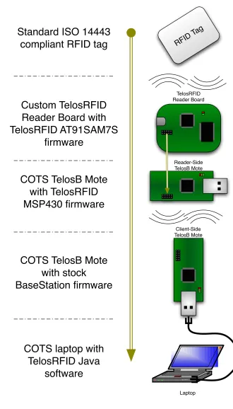
RFID Tag
Client-Side TelosB Mote Reader-Side TelosB Mote TelosRFID Reader Board
Standard ISO 14443
compliant RFID tag
Custom TelosRFID
Reader Board with
TelosRFID AT91SAM7S
firmware
COTS TelosB Mote
with TelosRFID
MSP430 firmware
COTS TelosB Mote
with stock
BaseStation firmware
COTS laptop with
TelosRFID Java
[image:26.612.129.459.97.675.2]software
4.3
Testability and Validation
For the TelosRFID system, a series of basic requirements are laid out and are used to
validate the performance of the system as a whole.
The boot sequence of the TelosRFID reader board can be viewed by connecting the
112500 baud DBGU port to an ASCII terminal program. The boot sequence is reported
in plaintext to verify that the system started up properly. Once the system is booted, its
continued operation is visibly established by a continuously blinking ”heartbeat” using the
green LED.
When the TelosRFID reader board detects a tag, it will communicate the detection
information to its attached TelosB mote via the DBGU port. In addition to the serial
com-munication, the reader board will toggle its red LED to visually indicate the detection and
communication.
When the reader-side TelosB mote receives a detection message interrupt from its
at-tached TelosRFID reader board, it will toggle its red LED. After queuing the message from
its UART port, it re-transmits it out to the ZigBee network. As it does this it also toggles
its blue LED. Because this is performed so quickly, both LEDs should appear to toggle at
the same time. Both LEDs toggling in unison visually indicate proper functionality of the
TelosB’s communications capabilities.
When the client-side TelosB mote receives a detection message from the ZigBee
net-work, it will communicate this detection to the USB port. In addition to the serial
commu-nication, it will toggle its LEDs to visually indicate receipt of the communication.
As the client PC receives a communication via the USB port, the Java application will
be waiting for messages from the ZigBee network. It detects the incoming message and
immediately displays information about the detection. When tag detections are displayed
in the PC’s console it validates that the communications chain is operating as expected. If
a detection is not displayed on the screen, then the previously described validation tools
Chapter 5
Hardware Implementation
The TelosRFID project involves several distinct hardware components. Most are
commeri-cially available off the shelf. This includes the following components:
• 13.56 MHz ISO/IEC 14443 compliant RFID tags
• Two (2) Crossbow Telos rev. B wireless sensor devices
• A client PC running a distribution of the Linux operating system
In addition to the COTS devices, an original custom hardware device was created as an
essential component of the TelosRFID system. Dubbed the TelosRFID Reader Board, its
design and firmware are significant contributions of this thesis.
5.1
Academic Contributions
The RFID tags used are commercial off the shelf components purchased from an RF
tech-nology retailer. They are not considered academic contributions in this thesis.
The TelosRFID tag reader board is a new, fully custom piece of hardware designed by
the author. It was designed in Altium DesignerTMusing component datasheets and several
reference designs[48, 49, 50]. Once designed, the PCB layout was submitted to Sunstone
Circuits for manufacture. After the PCB itself was made, the board was sent to Screaming
SMT (surface mount technology) techniques. The completed work is unique, useful, and
will contribute to the RFID and wireless research community by assisting with protocol
and process development. As detailed above, this custom hardware is needed in order to tie
together two distinct wireless technologies, RFID and WSN. It’s flexible programming and
communication features allow for research and applications that have previously not been
possible.
The TelosB wireless sensor devices used are commercial off the shelf components
pur-chased from an RF technology retailer. They are not considered academic contributions in
this thesis.
The client PC can be any standard desktop or laptop computer capable of running
Linux. They are not considered academic contributions in this thesis.
5.2
13.56 MHz ISO/IEC 14443 RFID tags
For the purpose of this thesis, 13.56 MHz ISO/IEC 14443 compliant RFID tags were
cho-sen. The specific type of tag used in the development of the communications software
stack is sold under the name Mifare Classic. The Mifare Classic 1k tags[51] were chosen
because they are based upon the ISO/IEC 14443 specification stack, are in widespread use
(over 1 billion tags)[52], and are readily available.
The ISO/IEC 14443 standard is used as an example RFID stack implementation due
to its well-defined specification[53, 54, 47, 55], as well as its widespread adoption in
industry[56, 52, 57, 58]. It provides an immediate practical use, while demonstrating
soft-ware layers used to access the hardsoft-ware. The example implementation developed for this
thesis provides an example framework for developing communication stacks. These
pro-grammable communication stacks can be implementations of existing standards, or could
be used to prototype 13.56 MHz RFID protocols that have yet to be developed or
5.3
TelosRFID Reader Board
The TelosRFID reader board is a custom piece of hardware that was developed specifically
for this thesis. The overarching goal behind the hardware design of the TelosRFID reader
board was to create a device that could be battery-powered, and entirely wireless. It had to
be able to detect 13.56 MHz RFID tags, and transmit that tag’s ID to the connected TelosB
mote. One of the most difficult design constraints is that is had to be incredibly small, so
as to permit portability.
5.3.1
Components
From a high level perspective, the TelosRFID reader board is a small circuit board with a
microcontroller and a 13.56 MHz wireless front-end integrated circuit (IC). The
microcon-troller (µC) used is an Atmel AT91SAM7S256 and the wireless front-end IC is a Philips NXP CL RC632. The microcontroller communicates via external interfaces in order to
fa-cilitate programming and communication, as well as communication with the CL RC632,
which powers and modulates the embedded antenna. The board also uses two power
man-agement ICs, the TPS61202 and the IRU1502-33, in order to negotiate voltage level
be-tween power sources and components which need to operate at different voltage levels. It
requires requires an external 5.0V power source in order to operate.
Atmel AT91SAM7S256
The Atmel AT91SAM7S256 is a 32-bit ARM-based RISC microcontroller[59]. It has the
following characteristics that make it a good choice for the TelosRFID platform.
• 256 Kb internal high-speed flash memory
• 64 Kb internal high-speed SRAM
• Advanced Interrupt Controller (AIC)
• Debug Unit (DBGU)
• Programmable Parallel Input/Output Controller (PIOA)
• USB 2.0 Full Speed Device Port
• 2 Universal Synchronous/Asynchronous Receiver Transmitters (USART)
• Master/Slave Serial Peripheral Interface (SPI)
• Two Wire Interface (TWI), usable as an I2C interface
• Small profile 64-pad QFN package
• at91lib - Atmel’s freely available C library for use onboard AT91 series
microcon-trollers
These varied properties each solved distinct design problems faced at the onset of this
thesis. The copious flash memory was needed in order to accommodate RFID protocol
stacks of varying complexity. Although the example firmware implementation provided
with this thesis takes up a fraction of this program space, it is not inconceivable that a more
complicated protocol, possibly one with layers of security and/or encryption, may demand
a significantly greater program footprint. Likewise with the SRAM, only a portion of the
provided 64 Kb was needed, but protocol implementations involving encryption algorithms
will use procedures that require much more memory to execute.
The PIT was used to drive the heartbeat of the TelosRFID board, as well as to control
all timing related functionality. Tying the PIT to the AIC permitted the implementation
of an LED heartbeat, without any modifications to the main loop of the program. The PIT
interrupt vector handler was also used to implement highly accurate and reliable time-based
functions, such as delays. The AIC, although not entirely necessary, served to make
can trigger an interrupt (i.e.external PIO pins, internal embedded peripherals), designing
interrupt-driven firmware became a simpler and more straightforward task. This results in
a system that is much more responsive in nature.
The DBGU, PIOA, USB 2.0, USART, SPI, and I2C peripherals are all I/O devices
capable of performing communications tasks. The original design was architected to
al-low as much redundancy of interfaces as possible. Because of the inavailabilty of dual
inline packages (DIP) for many components used, breadboarding a prototype was not a
reasonable option. The hardware was designed and implemented entirely by datasheet,
so redundancy and backup plans were always considered a high priority. A direct result
of this requirement was the selection of a microcontroller with numerous communications
interfaces to use and expose.
In the final implementation, the USB 2.0 port is used to power the board, using its 5
volt supply. The DBGU interface is used to program the microcontroller, as well as to
com-municate with the TelosB device. Additionally, when connected to a serial port at 115200
baud, the DBGU port can be used to view diagnostics from the system’s boot sequence, as
well as outgoing tag communications. The PIOA controller is used to control two output
pins on the AT91SAM7S256. Those output pins (PA7 and PA8) are used to pull up an
interrupt line on the connected TelosB. This signals to the TelosB that a communication is
about to arrive at its UART0 peripheral. The necessity of this interrupt line is discussed
further in section 5.4. The SPI interface is used for serial communication to and from the
NXP CL RC632 device. The USART and I2C peripherals were not ultimately needed for
the final deliverable, but a pin header to access the I2C is provided if users need it in order
to extend functionality.
The availability of a 64-pad QFN package for the AT91SAM7S256 allows for a very
small footprint on the board. With side dimensions of 9.0mm×9.0mm, this highly capable
The final point on the list is a publicly available free library called at91lib that is
pro-vided by Atmel for their AT91 series microcontrollers. This C library provides basic
ac-cessor functionality to most of the embedded peripherals in the chip. It also provides
ab-straction of some low level register accesses, reducing the possibility of errors during the
development cycle. The use of this library and its sample projects saved dozens of hours in
development time. It also undoubtedly improved the reliability of the firmware by shifting
the development focus from micro-implementation details to program flow and protocol
development. Since the library was open source, it ended up being modified. All NXP CL
RC632 communications functionality and ISO/IEC 14443 protocol stack implementations
were developed into the library framework.
Philips NXP CL RC632
The Philips NXP CL RC632 IC is a device meant to simplify the front-end design for 13.56
MHz RFID systems[60, 61]. It is a highly integrated RFID reader IC used for wireless
communication at 13.56 MHz. It supports every layer of the ISO/IEC 14443 protocol
stack, holistically or as distinct layers. That ability was essential for this thesis, as it allows
for the implementation of algorithms that use the standards-compliant ISO/IEC
14443-1[53] and ISO/IEC 14443-2[54] low level layers, while implementing custom higher level
layers. This is required in order to design and implement custom anti-collision algorithms
and communications protocols.
The CL RC632 is able to bi-directionally communicate with the AT91SAM7S256 using
an SPI bus, drastically reducing the number of traces, as compared to a parallel
commu-nication interface. Because the CL RC632 is digitally controlled, the microcontroller does
not have to directly manage the analog frontend. This abstraction allows the
microcon-troller to issue commands at its own pace, while the CL RC632 handles the strict wireless
timing requirements of RFID communication. This simplifies firmware design and makes
the implementation of computationally complex protocols and algorithms less challenging
The reader IC is important because it is a specialized chip designed to simplify the
ana-log design of the RF circuit. It ensures a clean, jitter-free 13.56 MHz baseband frequency,
and flexibly handles all of the modulation operations specified in ISO/IEC 14443-2[54].
To further simplify timing requirements on the microcontroller, the CL RC632 even has a
built in 64 byte send/receive buffer. This provides the AT91SAM7256 with the flexibility
to handle tag communications on its own timing schedule, even with performance delays.
In order to identify each reader board, every CL RC632 has a unique 32-bit serial
number. This serial number can be read via the SPI bus and can then be embedded into all
outgoing packets so that the client PC can identify exactly which TelosRFID board each
communication originated from.
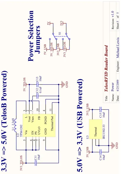
Texas Instruments TPS61202
The Texas Instruments TPS61202 IC is a charge pump voltage converter[50]. Its basic
pur-pose is to take in a power supply at 3.3V DC and output a power supply at 5V DC. The
original goal behind this choice was the desire to be able to power the entire TelosRFID
reader board off of the TelosB’s batteries. The boards have jumpers that were intended
to allow the reader board to change its power source back and forth between its onboard
USB port and the attached TelosB’s battery supply. Post-fabrication, this proved to be a
poor solution, as several problems crippled its success. The most significant
implementa-tion problem was power quality from the TPS61202 IC. The nature of a boost converter
is that it uses capacitors to store charge and then rapidly switches voltage sources in order
to increase output voltage to levels above it’s original input voltage. The problem with
a switching power supply is the transient line noise that it tends to produce. In the case
of the TPS61202, it oscillates between 1.25 MHz and 1.65 MHz, which will have
mas-sive negative repercussions on the analog front-end’s high frequency performance at 13.56
MHz.
Given 3V DC input from the TelosB device, the reader board will generate a 5V DC
RF wireless communication. As a result of this, the TelosRFID reader board must have its
own 5V DC power supply in order to operate as specified.
International Rectifier IRU1502-33
The International Rectifier IRU1502-33 is a linear regulator which converts power from
the USB’s 5V supply into a 3.3V supply needed by the microcontroller. Since it is a linear
regulator, rather than a switching charge pump, the supplied voltage is much cleaner than
that provided by the Texas Instruments TPS61202. This configuration is aided by the fact
that the 5V supplies used (PC USB host controller or a 5V battery pack) tend to be less
5.3.2
Electrical Schematics
The electrical design of the TelosRFID board was completed virtually, before it was ever
physically implemented. The two major obstacles to breadboard prototyping were the
ra-dio frequncies being used, as well as the lack of available components in through-hole
packages. Because of the electrical sensitivities associated with wireless RF frequencies, a
breadboard prototype could not be relied upon to give accurate results. Due to the
inavail-ability of most components in through hole (DIP) packages, breadboarding would not have
been possible without SMT adapter daughterboards. Because of the difficulty of prototype
SMT work, the decision was made to design the entire board using Altium Designer, an
electrical computer-aided design (CAD) tool.
The hardware circuitry, although custom designed, was somewhat derived from
ap-plication notes by Atmel, Philips NXP, and Texas Instruments[48, 49, 50]. Some of the
microcontroller portions of the board, including the USB 2.0 circuit were adapted from the
Atmel AT91SAM7S-EK evaluation board’s design files[48]. Likewise, the CL RC632
con-nectivity and RF tuning portions of the circuit were influenced by application notes from
Philips NXP[62, 49, 63, 61, 64].
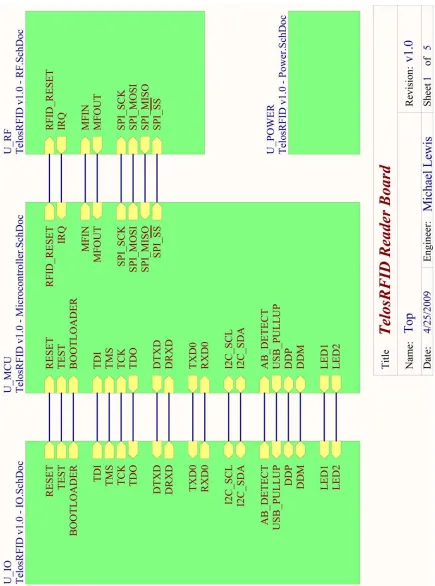
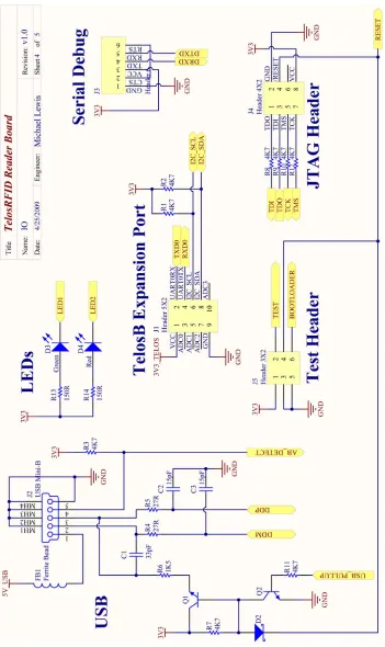
The following electrical schematics are organized into 5 diagrams, each representing a
Top Level View
The top level view shows how each of the subsystems are related to each other. As can
be seen, the microcontroller provides communication buses to the I/O subsystem. The
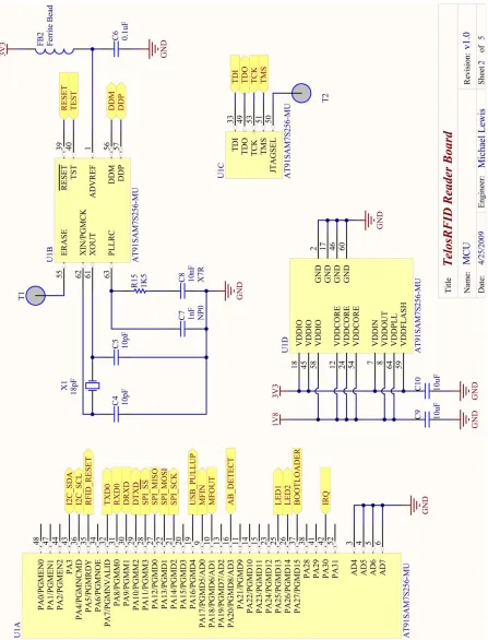
Microcontroller Circuitry
The microcontroller schematic shows what is needed to make the AT91SAM7S256
func-tion, as well as what external peripherals are used.
• The circuit on the left of the schematic (U1A) describes the I/O capabilities that are
used on the reader board. I2C [pins 36 & 43], USART0 [pins 31 & 32], DBGU
(USART) [pins 29 & 30], SPI [pins 21, 22, 27 & 28], USB 2.0 [pins 16 & 19], and
general purpose I/O pins [pins 9, 10, 25, 26, 35, 37 & 42] all provide the
capabil-ity for the microcontroller to communicate with other devices as well as to control
operations performed on the reader board.
• The circuit in the upper right of the schematic (U1B) is the clock/oscillator circuit,
which is responsible for generating a 48 MHz clock signal from crystal X1.
• The circuit on the lower right corner of the schematic (U1C) describes the JTAG
interface for the AT91SAM7S256 IC. Although it was not used in my development,
external pins are exposed so that future developers of the system can use the JTAG
interface to load and debug custom firmware.
• Finally, the circuit on the bottom-center (U1D) of the schematic describes the power
feeds upon which the microcontroller relies. The AT91SAM7S256 requires a 1.8V
and a 3.3V power supplies. It has a built-in 1.8V regulator so that it can generate its
own 1.8V supply (on pin 8, its VDDOUT). Decoupling capacitors are also included
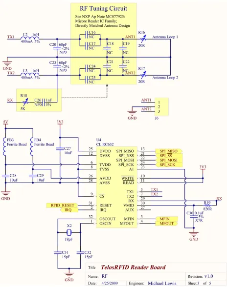
RF and CL RC632 Circuitry
The RF schematic breaks down into two sections: the CL RC632 connection diagram, and
the RF tuning circuit. The CL RC632 connection digram is relatively straightforward. The
SPI bus is used to communicate with the AT91SAM7S256, the IRQ line signals interrupts,
the RFID RESET line permits the microcontroller to power cycle the CL RC632, and the
MFIN and MFOUT lines expose low-level communication details. Aside from the crystal
oscillator and some power filtering components, there are very few parts needed in this
section.
One feature that was included in the hardware but has yet to be used in software is the
MFIN and MFOUT lines. These stand for ”MIFARE in” and ”MIFARE out” and they can
provide the capability to directly manipulate the data being sent and received from RFID
tags.
The RF tuning portion of the circuit is significantly more complicated than the
com-munications circuit. The RF circuit design incorporated knowledge from NXP[49] and
Fotopoulou[65]. The design procedure entailed constructing the circuit as shown, leaving
empty pads so that components whose values had yet to be determined could be placed at a
later time. After the boards were manufactured and populated, the antennas were measured
with respect to their inductance and impedance. Determining the values of the ”NC”
com-ponents involved applying formulas found in the aforementioned application note. These
formulas were based upon the measured impedance and inductance of the antenna trace.
The tuning procedure is outlined in [49, 62]. In short, it involves tuning capacitor and
resis-tor values on the board in order to obtain the lowest impedance and phase skew for the final
filter stage. Because the above documents are protected under non-disclosure agreements,
their details won’t be outlined here. If needed, they are available from Philips NXP, with
permission.
The final component values used were 10pF for C16 and C24, and 56pF for C18. C21.
C17, C25, C19, and C22 were left empty. These components were hand-soldered onto the
and R18 are potentiometers. Modifying their resistance will change behavioral
character-istics of the RF signal. The most dramatic effect is obtained by reducing the values of R16
and R17 to increase the output power. This occurs because the overall impedance of the
I/O Circuitry
The I/O schematic shows the interfaces that are externally exposed by the TelosRFID reader
board.
• The USB 2.0 port powers the reader board, and could theoretically be used to
com-municate with a host computer.
• Two LEDs are used to indicate the status of the board. The green LED is used as a
system heartbeat, with a 0.5 second period. The red LED is used to indicate RFID
tag activity, such as a transponder entering or leaving the reader’s field.
• The serial debug port is used to program the AT91SAM7S256. It is also used to print
boot information to a terminal, and to report tag activity to the attached TelosB mote.
• The JTAG header can be used to program and debug the microcontroller, if an
appro-priate JTAG device is available.
• Finally, the expansion port is used to expose multiple communications lines to
ex-ternal sources. From conception, it was originally designed to plug directly into the
attached TelosB mote. Due to compromises made during software development, this
is no longer the case. Several pins of this header are still used, but are connected with
Power Circuitry
The power schematic shows the wiring of the TPS61202 and IRU1502-33 power ICs
de-scribed in 5.3.1. It includes jumper pins which enable the user to configure where the
TelosRFID reader board would draw its power from. Since it has been determined that
TelosB sourced power does not perform as desired, these jumpers must be left connecting
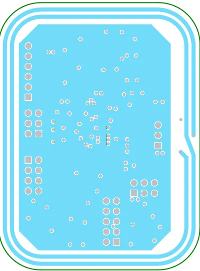
5.3.3
Board Layout
The TelosRFID Reader Board is a 4-layer PCB measuring 258in×11516in. The 4 layers, Top,
Ground, Power, and Bottom, are described in more detail in the following layout diagrams.
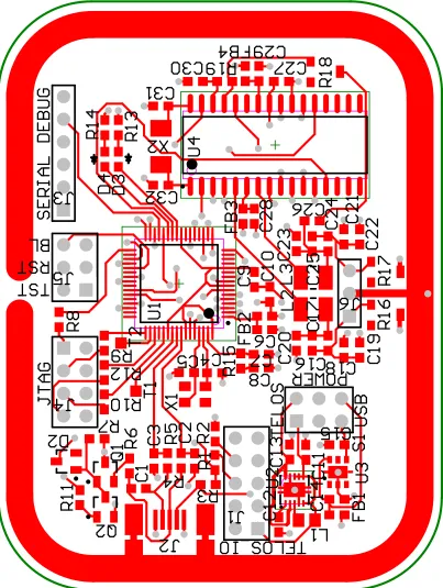
One interesting characteristic of the board that is not obvious from the previous
schemat-ics is that the antenna is actually formed using a copper PCB trace that surrounds the
func-tional circuit. The active portion of the antenna resides in the middle two layers of the
board. Each layer includes two loops of the antenna, for a total of four loops. The top and
bottom layer each include shields enclosing the active portion of the antenna. This helps to
reduce electrical noise produced by the board’s components from corrupting the wireless
signal emitted and recieived by the antenna.
The board itself was manufactured by Sunstone Circuits[66]. Sunstone Circuits
ac-cepted Gerber output files of the electronic design and manufactured a 4-sided PCB to
the required specifications. Once manufactured, the naked board, along with all necessary
components, was sent to Screaming Circuits[67] for PCB assembly. Screaming Circuits
also accepted Gerber files of the design and used them to accurately populate the PCB with
Top Layer
The top layer image includes the silkscreen layer, indicating the placement of components
on the board. All components are placed on the top, to avoid the complexity and cost of
double-sided board population. The top layer can be divided into two logical sections. The
center portion of the circuit consists of copper traces used to connect components together.
The trace that borders the circuit, however, is actually part of the ground net, and serves to
C1
P0C101 P0C102C2
P0C201 P0C202C3
P0C301 P0C302C4
P0C401 P0C402
C5
P0C501 P0C502C6
P0C601 P0C602
C7
P0C701 P0C702
C8
P0C801 P0C802
C9
P0C901P0C902
C10
P0C1001 P0C1002C11
P0C1101 P0C1102C12
P0C1201 P0C1202C13
P0C1301 P0C1302C14
P0C1401 P0C1402
C15
P0C1501 P0C1502C16
P0C1601 P0C1602C17
P0C1701P0C1702
C18
P0C1801 P0C1802
C19
P0C1901 P0C1902C20
P0C2001 P0C2002C21
P0C2101 P0C2102C22
P0C2201 P0C2202C23
P0C2301P0C2302
C24
P0C2401 P0C2402C25
P0C2501 P0C2502C26
P0C2601 P0C2602C27
P0C2701 P0C2702
C28
P0C2801 P0C2802C29
P0C2901 P0C2902C30
P0C3001 P0C3002C31
P0C3101 P0C3102C32
P0C3201 P0C3202D2
P0D201 P0D202 P0D203D3
P0D301 P0D302D4
P0D401 P0D402FB1
P0FB101 P0FB102FB2
P0FB201 P0FB202
FB3
P0FB301P0FB302
FB4
P0FB401 P0FB402J1
P0J101 P0J102 P0J103 P0J104 P0J105 P0J106 P0J107 P0J108 P0J109 P0J1010J2
P0J201 P0J202 P0J203 P0J204 P0J205P0J20MH1
P0J20MH2
P0J20MH3 P0J20MH4
J3
P0J301 P0J302 P0J303 P0J304 P0J305 P0J306J4
P0J401 P0J402
P0J403 P0J404
P0J405 P0J406
P0J407 P0J408
J5
P0J501 P0J502 P0J503 P0J504 P0J505 P0J506J6
P0J601 P0J602 P0J603L1
P0L101 P0L102L2
P0L201 P0L202
L3
P0L301 P0L302
Q1
P0Q101 P0Q102
P0Q103
Q2
P0Q201 P0Q202P0Q203
R1
P0R101P0R102
R2
P0R201
P0R202
R3
P0R301 P0R302
R4
P0R401 P0R402R5
P0R501 P0R502R6
P0R601 P0R602R7
P0R701 P0R702
R8
P0R801 P0R802R9
P0R901 P0R902R10
P0R1001 P0R1002R11
P0R1101P0R1102
R12
P0R1201 P0R1202R13
P0R1301 P0R1302R14
P0R1401P0R1402
R15
P0R1501 P0R1502R16
P0R1601 P0R1602 P0R1603R17
P0R1701 P0R1702 P0R1703R18
P0R1801 P0R1802 P0R1803R19
P0R1901 P0R1902S1
P0S101 P0S102 P0S103 P0S104 P0S105 P0S106T1
P0T101T2
P0T201U1
P0U101 P0U102 P0U103 P0U104 P0U105 P0U106 P0U107 P0U108P0U109 P0U1010
P0U1011 P0U1012 P0U1013 P0U1014 P0U1015 P0U1016 P0U1017 P0U1018 P0U1019 P0U1020 P0U1021 P0U1022 P0U1023 P0U1024 P0U1025 P0U1026 P0U1027 P0U1028 P0U1029 P0U1030 P0U1031 P0U1032 P0U1033 P0U1034 P0U1035 P0U1036 P0U1037 P0U1038 P0U1039 P0U1040 P0U1041 P0U1042 P0U1043 P0U1044 P0U1045 P0U1046 P0U1047 P0U1048
P0U1049 P0U1050 P0U1051 P0U1052 P0U1053 P0U1054 P0U1055 P0U1056 P0U1057 P0U1058 P0U1059 P0U1060 P0U1061 P0U1062 P0U1063 P0U1064
U2
P0U201 P0U202 P0U203 P0U204 P0U205
P0U206
P0U207
P0U208
P0U209
P0U2010 P0U2011
U3
P0U301 P0U302 P0U303P0U304
P0U305
P0U306 P0U307
U4
P0U401 P0U402 P0U403 P0U404 P0U405 P0U406 P0U407 P0U408 P0U409 P0U4010 P0U4011 P0U4012 P0U4013 P0U4014 P0U4015 P0U4016
P0U4017 P0U4018 P0U4019 P0U4020 P0U4021 P0U4022 P0U4023 P0U4024 P0U4025 P0U4026 P0U4027 P0U4028 P0U4029 P0U4030 P0U4031 P0U4032
X1
P0X100P0X101 P0X102
X2
P0X201 P0X202 P0U1028 P0U4021 P0C901 P0U108 P0U1012 P0U1024P0U1054 P0U1058 P0U1064
P0C1001 P0C2701 P0FB202 P0J303 P0J408 P0J501 P0Q103 P0R102 P0R202 P0R302 P0R702 P0R1301 P0R1401 P0S103 P0U107 P0U1018 P0U1045 P0U1059
P0U4010 P0U4011
P0U4025 P0C1101 P0J101 P0L101 P0S101 P0U205 P0U206 P0U207 P0U208 P0C1501 P0S105 P0U304 P0FB302 P0FB402 P0S104 P0C1301 P0S102 P0U202 P0U2010 P0C1401 P0FB102 P0S106 P0U306 P0J204 P0R301 P0U1016 P0C1602 P0C1702
P0C1801 P0C1901
P0J601
P0R1601
P0C2102 P0C2202
P0C2402
P0C2502
P0J603 P0R1701 P0J506
P0U1037
P0C302 P0R401
P0U1056 P0C202 P0R501 P0U1057 P0J304 P0U1030 P0J305 P0U1029 P0C201 P0C301 P0C402 P0C502 P0C602 P0C702 P0C802 P0C902 P0C1002
P0C1102
P0C1202
P0C1302
P0C1402 P0C1502
P0C1802 P0C1902
P0C2002
P0C2101 P0C2201
P0C2301 P0C2702 P0C2802 P0C2902 P0C3002 P0C3102 P0C3202 P0J109 P0J205 P0J20MH1 P0J20MH2
P0J20MH3 P0J20MH4 P0J301 P0J402 P0J503 P0J505 P0J602 P0Q202 P0R1602 P0R1702 P0U102 P0U103 P0U104 P0U105 P0U106 P0U1017 P0U1046 P0U1060 P0U204
P0U209 P0U2011
P0U302
P0U307 P0U408 P0U409 P0U4012
P0U4023 P0U4028 P0J106 P0R101 P0U1036 P0J108 P0R201 P0U1043 P0U1042 P0U402 P0D302 P0U1025 P0D402 P0U1026 P0U109 P0U403 P0U1010 P0U404 P0C101 P0J202 P0R402 P0C102 P0J203 P0R502 P0R602 P0C401 P0U1062 P0X101 P0C501 P0U1061 P0X102 P0C601 P0FB201 P0U101 P0C701 P0R1502 P0U1063 P0C801 P0R1501 P0C1201 P0U201 P0C1601 P0C1701 P0C2001 P0L202
P0C2302 P0C2501 P0C2401 P0C2602 P0L302 P0C2601 P0R1802 P0C2801 P0FB301 P0U406 P0C2901 P0FB401 P0U4026
P0C3001 P0R1902
P0U4030 P0C3101 P0U4032 P0X201 P0C3201 P0U401 P0X202 P0D201 P0Q101 P0Q203 P0R701 P0D301 P0R1302 P0D401 P0R1402 P0FB101 P0J201 P0J401 P0R802 P0J403 P0R902 P0J405 P0R1002 P0J407 P0R1202 P0L102 P0U203 P0Q102 P0R601 P0Q201 P0R1102 P0T101 P0U1055 P0T201 P0U1050 P0D203 P0J404 P0J504 P0U1039 P0U1035 P0U4031 P0R1801 P0R1901 P0U4029 P0J104
P0U1031 P0U1027
P0U4013 P0U1022 P0U4022 P0U1021 P0U4024 P0R1001 P0U1053 P0R801 P0U1033
[image:50.612.109.512.130.665.2]P0R901 P0U1049 P0J502 P0U1040 P0R1201 P0U1051 P0L201 P0U405 P0L301 P0U407 P0J102 P0U1032 P0R1101 P0U1019
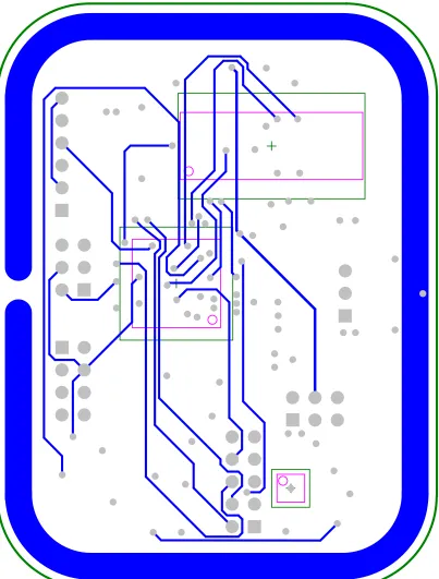
Ground Layer
The layer just below the top layer in the board is the ground layer. The ground layer
can be divided into two logical sections as well. The center portion of the circuit forms
a ground plane that is used underneath the entire component portion of the board. This
provides shielding between the top and bottom layers for high frequency signal traces,
as well as providing a low resistance, loop free means of grounding all components at the
same voltage potential. This low resistance is important for reducing electrical noise within
the board. The trace that borders the circuit, although logically part of the ground net, is
actually one half of the 13.56 MHz antenna used to communicate with RFID tags. This
P0C201 P0C301 P0C402 P0C502 P0C602 P0C702 P0C802 P0C902 P0C1002
P0C1102
P0C1202
P0C1302
P0C1402 P0C1502
P0C1802 P0C1902
P0C2002
P0C2101 P0C2201
P0C2301 P0C2702 P0C2802 P0C2902 P0C3002 P0C3102 P0C3202 P0J109 P0J205 P0J20MH1 P0J20MH2
P0J20MH3 P0J20MH4 P0J301 P0J402 P0J503 P0J505 P0J602 P0Q202 P0R1602 P0R1702 P0U102 P0U103 P0U104 P0U105 P0U106 P0U1017 P0U1046 P0U1060 P0U204
P0U209 P0U2011
P0U302
P0U307 P0U408 P0U409 P0U4012
P0U4023
[image:52.612.110.511.131.667.2]P0U4028
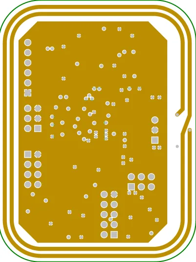
Power Layer
The layer just below the ground plane in the board is the power layer. The power layer
can also be divided into two logical sections. The center portion of the circuit forms a
3.3V power plane that is used underneath the entire component portion of the board. This
provides shielding between the top and bottom layers for high frequency signal traces, as
well as providing a low resistance, loop free means of powering all 3.3V components at
the same voltage potential. This low resistance is important for reducing electrical noise
within the board. The trace that borders the circuit, although logically part of the ground
net, is actually the second half of the 13.56 MHz antenna used to communicate with RFID
P0C201 P0C301 P0C402 P0C502 P0C602 P0C702 P0C802 P0C902 P0C1002
P0C1102
P0C1202
P0C1302
P0C1402 P0C1502
P0C1802 P0C1902
P0C2002
P0C2101 P0C2201
P0C2301 P0C2702 P0C2802 P0C2902 P0C3002 P0C3102 P0C3202 P0J109 P0J205 P0J20MH1 P0J20MH2
P0J20MH3 P0J20MH4 P0J301 P0J402 P0J503 P0J505 P0J602 P0Q202 P0R1602 P0R1702 P0U102 P0U103 P0U104 P0U105 P0U106 P0U1017 P0U1046 P0U1060 P0U204
P0U209 P0U2011
P0U302
P0U307 P0U408 P0U409 P0U4012
P0U4023
[image:54.612.110.511.126.669.2]P0U4028
Bottom Layer
The layer on the underside of the board, the bottom layer, can be divided into two logical
sections. The center portion of the circuit consists of copper traces used to connect
com-ponents together. The trace that borders the circuit is actually part of the ground net, and
P0U1028 P0U4021 P0FB302 P0FB402 P0S104 P0J204 P0R301 P0U1016 P0J304 P0U1030 P0C201 P0C301 P0C402 P0C502 P0C602 P0C702 P0C802 P0C902 P0C1002
P0C1102
P0C1202
P0C1302
P0C1402 P0C1502
P0C1802 P0C1902
P0C2002
P0C2101 P0C2201
P0C2301 P0C2702 P0C2802 P0C2902 P0C3002 P0C3102 P0C3202 P0J109 P0J205 P0J20MH1 P0J20MH2
P0J20MH3 P0J20MH4 P0J301 P0J402 P0J503 P0J505 P0J602 P0Q202 P0R1602 P0R1702 P0U102 P0U103 P0U104 P0U105 P0U106 P0U1017 P0U1046 P0U1060 P0U204
P0U209 P0U2011
P0U302
P0U307 P0U408 P0U409 P0U4012
P0U4023 P0U4028 P0J106 P0R101 P0U1036 P0J108 P0R201 P0U1043 P0U1042 P0U402 P0U109 P0U403 P0U1010 P0U404 P0FB101 P0J201 P0J302 P0J306 P0D203 P0J404 P0J504 P0U1039 P0U1035 P0U4031 P0J104
P0U1031 P0U1022
[image:56.612.110.513.128.659.2]P0U4022 P0U1021 P0U4024 P0J502 P0U1040 P0J102 P0U1032 P0R1101 P0U1019
5.4
Telos rev. B Mote
The Telos rev. B (TelosB) device is a freely available wireless sensor mote[68]. It was
de-signed by the University of California, Berkeley, and subsequently released to the public as
a free design[69]. Implemented physical boards are available from several manufacturers[70,
42] and are readily available as a commercial off the shelf (COTS) product.
The TelosB mote was originally intended to perform the role of a sensor data capture
device. It has built in sensors for monitoring temperature, light, and humidity, as well as
including an expansion port to facilitate the use of additional third party or custom sensor
module[42]. This sensor data is generally then transmitted over the built-in IEEE 802.15.4
compliant wireless radio[71]. All of this functionality is controlled by a low-power
16-bit MSP430F1611 microcontroller, manufactured by Texas Instruments[72, 73]. The mote
Chapter 6
Software/Firmware Design
6.1
Academic Contributions
As part of this thesis, the TelosRFID project involves several software components that are
unique academic contributions.
The TelosRFID Reader Board firmware is a suite of original embedded software for
the Atmel AT91SAM7S256 microcontroller. It’s source code was written in the ANSI C
programming language. It was built as a collaboration of several custom software modules,
structured to make use of the low-level open-source library at91lib[74], released by the
Atmel CorporationR. Several unique firmware contributions are delivered in support of
this thesis. The most significant of these contributions is an original ISO/IEC 14443 RFID
communication stack implementation, a tag pressence management methodology, and an
iterrupt-driven wired communication protocol design.
The reader-side TelosB firmware is a suite of original embedded firmware for the Texas
Instruments MSP430 microcontroller. The firmware source code was written in the NesC
programming language. It was built as a collaboration of several custom software modules,
structured on top of the TinyOS[75] framework and operating system. The TinyOS
devel-opment ecosystem was produced by the University of California, Berkeley. The unique
contribution built into this framework is an original interrupt-driven wired
reader board, without corrupting wireless communications. Additionally, this
communi-cation protocol uses the TinyOS ZigBee library in order to broker messages between the
TelosRFID reader and the ZigBee wireless network.
The client-side TelosB software is not an original contribution. The client-side TelosB
uses the BaseStation application that is included in the standard TinyOS distribution.
The client-side application software is an original Java program that communicates with
the attached TelosB mote. It leverages TinyOS libraries in order to read mote traffic and
6.2
TelosRFID Reader Board Firmware
The TelosRFID firmware resides in the flash memory of the AT91SAM7S256
microcon-troller. It is responsible for coordinating all functionality on the reader board. The firmware
itself is written in C, and is debugged, compiled and linked through the YAGARTO tool
chain[76]. It is responsible for several tasks.
The TelosRFID firmware controls the RFID air protocol implementation. It realizes
the ISO-IEC 14443-2 and ISO/IEC 14443-3 protocol logic necessary to communicate with
MIFARE tags. The firmware accomplishes this through digital control of the CL RC632
IC. A CL RC632 driver was written to interface with the RF frontend. It consists of several
layers, from basic read/write of registers, up to higher-level functions, such as configuring
the RF control settings. Built on top of the RC632 driver is an ISO/IEC 14443 driver. This
protocol driver leverages the low level control functions of the RC632 driver in order to
im-plement the ISO/IEC 14443 RFID air protocol, including tag detection and anti-collision.
The TelosRFID firmware also controls other onboard functionality. It controls board
initialization, including setting up the microcontroller’s ports, the onboard timer module
and drivers, and printing out boot diagnostics via the DBGU port. It produces the green
LED heartbeat, and toggles the red LED during tag detection. Additionally, it runs the
routine which continuously scans the air for nearby tags, and reports its findings to the
RFID tag presence monitoring module (TagMonitor). The TagMonitor module was written
for this thesis in order to keep track of what tags are present near the reader. When a tag
first enters the reader’s field it is reported to the TagMonitor, and a ”tag found” message is
sent to the central PC. This is considered the tagenteringthe reader’s proximity. The air is
then continuously scanned for tags, every time the original tag reports back, its ID is sent
to the tag monitor. As long as the tag’s ID keeps being reported to the TagMonitor, it is