Contents lists available atScienceDirect
Solar Energy Materials and Solar Cells
journal homepage:www.elsevier.com/locate/solmat
Anodic oxidations: Excellent process durability and surface passivation for
high efficiency silicon solar cells
N.E. Grant
a,∗, T.C. Kho
b, K.C. Fong
b, E. Franklin
c, K.R. McIntosh
d, M. Stocks
b, Y. Wan
b,
Er-Chien Wang
e, N. Zin
f, J.D. Murphy
a, A. Blakers
baSchool of Engineering, University of Warwick, Coventry, CV4 7AL, United Kingdom
bResearch School of Engineering, The Australian National University, Canberra, ACT, 0200, Australia cSchool of Engineering, University of Tasmania, Hobart, Tasmania, 7001, Australia
dPV Lighthouse, Coledale, NSW, Australia
ePVcomB, Helmholtz-Zentrum Berlin, Schwarzschildstr. 3, 12489, Berlin, Germany fThe College of Optics and Photonics, University of Central Florida, Orlando, FL, United States
A R T I C L E I N F O
Keywords:
Anodic oxidation Silicon Silicon dioxide Solar cell Surface passivation
A B S T R A C T
We investigate the versatility of anodically grown silicon dioxide (SiO2) films in the context of process durability
and exceptional surface passivation for high efficiency (> 23%) silicon solar cell architectures. We show that a room temperature anodic oxidation can achieve a thickness of ~70 nm within ~30 min, comparable to the growth rate of a thermal oxide at 1000 °C. We demonstrate that anodic SiO2films can mask against wet chemical
silicon etching and high temperature phosphorus diffusions, thereby permitting a low thermal budget method to form patterned structures. We investigate the saturation current densityJ0of anodic SiO2/silicon nitride stacks
on phosphorus diffused and undiffused silicon and show that aJ0of < 10 fA cm−2can be achieved in both cases.
Finally, to showcase the anodic SiO2films on a device level, we employed the anodic SiO2/silicon nitride stack to
passivate the rear surface of an interdigitated back contact solar cell, achieving an efficiency of 23.8%.
1. Introduction
The development of versatile dielectric coatings is of great interest for photovoltaics, especially as the industry is seeking methods to boost the efficiency of solar cells while maintaining or even reducing manu-facturing costs. Specifically, thermal silicon dioxide (SiO2) is one
ex-ample where a single dielectric film can be extremely versatile. In particular, thermal SiO2 is used to electrically passivate the silicon
surface [1,2], act as a barrier against wet chemical etching and thermal diffusions [3,4], mitigate potential induced degradation [5], insulate conducting layers from each other, and be applied as a passivated contact [6]. However, thermal oxidations require very high tempera-tures (~1000 °C) and long oxidation times (i.e. > 30 min), which de-tracts from their benefits. The high temperatures pose a risk of per-manently degrading the bulk minority carrier lifetime and the high thermal budget can be expensive for commercial solar cells. For these reasons, there has been research on developing alternative approaches of growing SiO2that retain the same versatile qualities of thermal SiO2,
but which are grown at much lower temperatures [7]. Anodisation of silicon to grow silicon dioxide at room temperature is one promising
approach for PV applications [8,9].
Anodisation is a simple process whereby silicon wafers are im-mersed in an electrolyte (e.g. nitric acid) and a positive voltage is ap-plied to the wafer relative to a counter electrode (e.g. a platinum wire) [10]. When a voltage is applied, oxygen-containing species (H2O, O2−,
OH−) in the solution are forced to the positively biased silicon wafer
where they oxidise the silicon surface and form a silicon dioxide film. Without the applied voltage, the formation of silicon dioxide is very slow and the thickness of the film cannot be controlled. Anodisation of silicon can be carried out under constant potential or constant current, each having their advantages and disadvantages. Under constant cur-rent operation, the voltage typically increases with oxide thickness, and in some cases can exceed 100 V [11]. This type of oxidation can form very thick oxides (> 100 nm), but is generally quite aggressive and thus susceptible to pit/defect formation [10]. Under constant potential op-eration, the current typically decreases as the oxide thickness increases. Although the oxidation rate is much slower under constant potential, the oxidation process is safer to operate. One could also speculate that a less aggressive oxidation in this case would also limit the pit/defect formation.
https://doi.org/10.1016/j.solmat.2019.110155
Received 14 January 2019; Received in revised form 7 May 2019; Accepted 26 August 2019 ∗Corresponding author.
E-mail address:[email protected](N.E. Grant).
Available online 06 September 2019
0927-0248/ © 2019 The Authors. Published by Elsevier B.V. This is an open access article under the CC BY license (http://creativecommons.org/licenses/by/4.0/).
face properties, Cui et al. developed a light induced anodisation method, which permits single side anodic oxide growth, and was able to reduce theDitof the oxide down to 6 × 10¹¹eV−1cm−2[15,16].
Re-cently Grant et al., examined the benefits of capping the room tem-perature grown anodic SiO2film with a low-pressure chemical vapour
deposition (LPCVD) silicon nitride (Si3N4) film [17]. When capped, the
interface properties of the anodic SiO2film revealed a very lowDitand
charge density of ~2 × 10¹⁰eV−1cm−2and ~2 × 1011cm−2
respec-tively, corresponding to anSof less than 3 cm s−1(at Δn= 1015cm−3)
or a surface saturation current density of 3 fA cm−2[17]. Despite the
significant improvements in anodic oxide passivation over the past decade, the compatibility of the oxide in a solar cell fabrication process and the retention of surface passivation quality have yet to be a de-monstrated on a device level.
In this work we examine the versatility of room temperature grown anodic SiO2in the context of fabricating silicon solar cells. We examine
the growth kinetics of the anodic SiO2film on diffused and undiffused
silicon, and we assess their ability to mask against wet chemical silicon etching and high temperature phosphorus diffusions. We then examine the impact of the SiO2thickness on the saturation current densityJ0for
diffused and undiffused silicon wafers. Finally, to demonstrate the ro-bustness of the anodic SiO2films, we have fabricated a 23.8% efficient
interdigitated back contact (IBC) solar cell employing the anodic SiO2
layer to passivate the rear surface of an IBC cell.
2. Experimental Methods
Anodic oxidations were performed on (100) orientedn-type float-zone (FZ) silicon wafers with a diameter of 100 mm. For clarity, the thickness and resistivity of the wafers are described in the text. The wafers received an HF:HNO3(1:10) etch for 3 min to remove saw
da-mage from their surfaces and were subsequently cleaved in half unless otherwise specified. The cleaved samples were then RCA cleaned using the standard procedure as outlined by Kern et al. [18], and etched in a 5% HF solution to remove the wet chemical oxide grown during the cleaning procedure.
Thermal diffusion of selected samples was performed in a Tempress 5-inch quartz tube furnace. In order to achieve a sheet resistance of 100 ± 20 Ω/sq, phosphorus diffusions were conducted at 850 °C for 20 min while the boron diffusions were performed at 890 °C for 80 min. Following the thermal diffusions, the phosphosilicate and borosilicate glasses were removed in 5% HF. The diffused samples were subse-quently RCA cleaned and given a final 5% HF dip prior to anodisation. Anodic oxidations were performed by applying a +30 V bias across a silicon wafer and platinum wire electrode immersed in a 20% HNO3
solution (at room temperature), where the silicon wafer was held at the higher potential. In order to connect the silicon sample electrically via an alligator clip, the top half was not immersed in the HNO3, meaning
only half of each sample was anodically oxidised. Unless otherwise
Under constant potential, the oxidation kinetics during anodisation can exhibit substantially different growth rates depending on the electrolyte (composition, concentration and temperature), silicon ma-terial (type and doping concentration), applied voltage and illumina-tion intensity [10,22]. For the purpose of this study, we fix the voltage at 30 V, we use a 20% HNO3solution as the electrolyte and the
illu-mination intensity is determined by the fluorescent light housed in the fumehood, consistent with previous work [12,17]. Our focus is to un-derstand how the silicon material properties influence the oxidation kinetics and how this might be useful in the context of silicon solar cells (i.e. masking purposes and/or surface passivation).
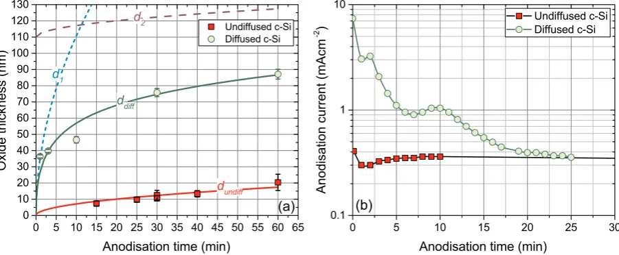
Fig. 1a plots the oxide thickness versus time for undiffused and diffused silicon grown at room temperature. For undiffused silicon, the increase in oxide thicknessd(t)with oxidation time can be expressed as a parabolic [10,23];
= +
d t( ) d0 a t (1)
whereacorresponds to the anionic properties of the oxide layer. For the purpose of this discussion we assume an initial oxide thickness of d0= 0 nm. By fitting Eq. (1) to the undiffused data in Fig. 1a, we
achieve an excellent fit whena= 2.25, which after taking the deriva-tive of Eq.1, corresponds to an oxidation rate of 1 nm/min att= 1 min and 0.15 nm/min att= 60 min. To understand why the oxidation rate is relatively slow on undiffused c-Si, we must first understand the basic kinetics during anodisation of c-Si.
The growth of silicon dioxide on silicon requires the diffusion and/ or drift of oxygen species (anions) through the oxide film, i.e. ionic current. Considering that our oxidations are performed at room tem-perature, one could assume that diffusion of oxygen-containing anions is too slow to account for the oxide growth rates observed in this work [10]. In this regard, inward movement/migration of the oxygen source must be field-assisted, which is primarily determined by the field strength (i.e. voltage across the oxide) [10]. Assuming the measured current during anodisation is ionic, and that its magnitude depends on the field strength across the oxide,Fig. 1b (red squares) indicates that the field strength in the undiffused c-Si case must be relatively weak, evident by the low ionic current (0.3–0.4 mA cm−2) measured during
anodisation. Notably, we do not attribute the low ionic current to a high contact resistance between the metal clip and silicon wafer, because in our previous work it was demonstrated that an increase in voltage from 30V to 60V did not increase the anodisation current, indicating the current is limited by the oxidation kinetics and not the contact re-sistance [24].
(~100 Ω/sq) silicon wafer during anodisation. At timet= 0 min, the current is very high relative to undiffused c-Si (8 mA cm−2), and this
rapidly declines over the first few minutes. This behaviour indicates the field strength across the growing oxide must be higher than in the undiffused case, however the cause for this enhancement is not well understood at this time. Nevertheless, we can still draw some mean-ingful insight regarding the potential mechanism(s) giving rise to the higher oxidation rates on diffused silicon. Firstly, the oxidation of si-licon during anodisation requires a reaction with a hole from the va-lance band at the silicon surface [10], meaning the mechanism by which holes can react at the silicon surface has been enhanced, e.g. accumulation of holes at the c-Si surface or injection of electrons into the conduction band via reactions with the electrolyte. Secondly, it is also possible that surfaces states arising from highly diffused phos-phorus and boron (not shown) surfaces enhance one, or both of these mechanisms via generation-recombination centres [10,25].
Fort> 10 min, the oxidation rate appears to slow rapidly, i.e. from ~10 nm/min att= 1 min to 1.5 nm/min att= 10 min. Thus contrary to undiffused silicon, where the oxide thickness follows a steady para-bolic trend with time, oxidation on diffused silicon does not behave in a similar manner. Therefore in order to accurately fit the data for diffused c-Si inFig. 1a, it is necessary to treat the oxidation growth as a two-step process, i.e. two parabolic trends. In the initial stages of oxidation, the oxide thicknessd1can be expressed as,
= =
d t1( ) 35 t (withd0 0 nm) (2)
however after some minutes of oxidation, the cause for this ex-ceptionally high growth rate≫1 nm/min, transitions to a much slower one (< 1 nm/min), i.e. equivalent to that for undiffused silicon,
= +
d t2( ) 110 2.25 t (3)
having established fitting parameters for each of the parabolic expres-sions, d1 and d2 must be inversely summed to calculate the oxide
thickness with time for diffused c-Si, where;
= +
= ++ +
d t
yields,
( ) d d d
diff t t t
1 1 1
2 . 25 35 35 110 (2 . 25 35) 110
diff 1 2
(4) the expression derived in Eq. (4)allows us to predict the oxidation thickness and rate on diffused silicon for the conditions described in
this work, however we do expect this trend to vary depending on ma-terial properties and anodic oxidation conditions (voltage, electrolyte, temperature, etc). Thus, while fitting the data using the inverse sum of two parabolic expressions is robust, individual fitting parameters will need to be determined using experimental data corresponding to spe-cific conditions in which the anodic oxidation is being performed.
From our examination of anodic oxide growth on diffused and un-diffused c-Si, it is clear a wide range of oxide thicknesses under well controlled conditions can be achieved. We now assess their robustness in the context of masking against thermal diffusions and wet chemical etching for PV applications.
3.2. Masking durability of anodically grown SiO2films
In this work we examine whether anodically grown silicon dioxide films can mask against phosphorus during a thermal diffusion process, which could be useful in the context of high efficiency cell designs, e.g. IBC solar cells, where masking is required to protect locally diffused regions. Notably, we have not examined masking against boron be-cause, as elucidated in Ref. [4], boron diffuses much slower than phosphorus through an SiO2film, thus the barrier oxides developed in
this work should also be applicable to masking against boron. Firstly, an FZ > 100 Ω cmn-type wafer was subject to a boron diffusion, yielding a sheet resistance of ~100 Ω/sq as outlined in the Experimental Methods section. Following the boron diffusion, half of the boron diffused sample was anodically oxidised for 30 min resulting in an oxide thickness of ~70 nm. Subsequently, the sample (half oxi-dised and half bare c-Si) was subject to a phosphorus diffusion in a quartz tube furnace at 850 °C for 20 min. Following the phosphorus diffusion, the anodic SiO2film and phosphosilicate glass were removed
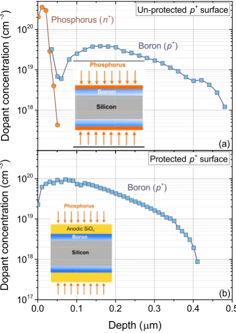
in 10% HF. To determine if phosphorus did penetrate the anodic oxide film during the diffusion step, an electrochemical capacitance voltage (ECV) technique was used to measure the boron and phosphorus con-centrations in the silicon wafer.Fig. 2plots the results.
FromFig. 2a, which plots the dopant concentration of an un-pro-tected sample, the ECV measurement deun-pro-tected a high concentration of phosphorus and boron in the near surface region of the sample. How-ever in Fig. 2b, which plots the dopant concentration for a sample protected by a thick (70–80 nm) anodic SiO2film, the ECV
[image:3.595.73.524.57.243.2]measure-ment could only detect boron. Our ECV results therefore indicate the anodic SiO2film did prevent phosphorus from diffusing through the
Fig. 1.(a) Oxide thickness versus anodisation time on undiffusedn-type silicon (red squares) and phosphorus diffused (~100 Ω/sq) silicon (green circles).dundiff(red
line) andddiff(green line) correspond to parabolic trends which approximate the oxide thickness as a function of anodisation time for undiffused and diffused silicon
respectively. In the case forddiff, the inverse sum of two parabolic trendsd1(dashed blue line) andd2(dashed purple line) was required to model the oxide thickness
film into the silicon sample. Notably, although the oxides were initially grown at room temperature, they were subject to high temperatures before, and during the thermal diffusion process, meaning the anodic oxides become more like thermal oxides, whereby effusion of OH−
from the SiO2network results [22]. In this regard, it should be expected
that thick anodic SiO2 films form a good barrier against impurity
(TMAH) solution. In this case the diffusion provides sufficient surface passivation to yield a PL signal. It is important to note that the anodic oxide (protected region inFig. 3a) has not been thermally treated, and thus is not providing a notable level of surface passivation. In this case, the higher PL intensity arising from the anodic oxide results because defect states within the oxide layer are luminescing at similar wave-lengths to the silicon, and does not result from additional surface pas-sivation [10]. Therefore any reduction in the effective lifetime would imply the diffusion has been etched.
[image:4.595.44.282.56.391.2]In order to quantify how well the oxide protects the diffusion during wet chemical etching, we measure both the effective lifetime and PL intensity. Etching the sample for 12 min in TMAH allows sufficient time to remove the diffusion from the unprotected part of the sample, which is evident by the very low PL signal shown inFig. 3b, indicating that all passivation resulting from the diffusion has been lost. Further etching of the sample does not change the behaviour (PL and lifetime signal) of the unprotected region. In contrast, etching the protected region for 12 or even 36 min does not significantly alter the PL signal and effective lifetime, indicating that the surface passivation remains unchanged and hence the diffusion remains intact. However, after thoroughly rinsing the sample in DI water and storing in a petri-dish for 24 h, the silicon surface underwent some surface modifications whereby the diffusion has been slightly etched, evident by the change in PL uniformity and effective lifetime measurement. This suggests that although the sample was thoroughly rinsed prior to storing the sample, it still contained TMAH residue within the SiO2film.
[image:4.595.102.485.544.699.2]Fig. 2.ECV doping profile measurements of a boron diffused c-Si sample (a) un-protected and (b) un-protected by a thick anodic oxide film (~70 nm) during a subsequent phosphorus diffusion process. Blue squares and orange circles cor-respond to boron and phosphorus dopants respectively. (For interpretation of the references to colour in this figure legend, the reader is referred to the Web version of this article.)
3.3. Surface passivation of diffused and undiffused silicon surfaces
In our examination of anodically grown SiO2films thus far, we have
focused on applications in which these oxides can be used to alleviate high temperature processing to form masking barriers during wet chemical etching and thermal diffusions. Here we examine the cap-ability of anodic SiO2films to passivate the c-Si surface, and thus their
permanent use in c-Si solar cells.
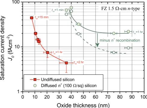
Fig. 4plots the saturation current densityJ0versus oxide thickness
after the deposition of LPCVD Si3N4. In this case, the addition of the
Si3N4layer was necessary to achieve a very high level of surface
pas-sivation and to mitigate moisture ingression, as demonstrated in Ref. [17]. Notably, the surface passivation of the anodic oxide partly ben-efits from the high temperature (~780 °C) LPCVD deposition, but as demonstrated previously, a 400 °C without the Si3N4 layer can also
result in good surface passivation [9,12,13]. Another benefit of using LPCVD Si3N4 on top of the anodic SiO2 was to enable a direct
sub-stitution for the thermal SiO2/LPCVD Si3N4stack in our existing IBC
fabrication process, where previously we had achieved a certified effi-ciency of 24.4% [26]. InFig. 4, theJ0was determined from the slope of
the inverse lifetime using the method of Kane and Swanson [27], which was measured by the PCD method [28]. The vertical error bars inFig. 4 represent the uncertainty inJ0when accounting for variations in the
bulk lifetime (e.g. when intrinsic defect recombination is more domi-nant than Auger), as measured by the light-enhanced HF passivation technique [29,30]. The horizontal error bars represent the spatial var-iation in oxide thickness across each sample.
Fig. 4demonstrates that for both diffused and undiffused silicon samples, theJ0decreases with increasing oxide thickness. In the case
for undiffused silicon (red squares), the J0 decreases from 45 to
4.5 fA cm−2for an oxide thickness of 7 and 36 nm respectively, while
for diffused silicon (green circles), the J0 decreases from 70 to
20 fA cm−2for an oxide thickness of ~40 and > 70 nm respectively.
The absolute oxide thickness therefore does not appear to govern the level of surface passivation, but rather the oxidation time. In a previous publication (on undiffused c-Si) it was shown that as the oxide thickness
increased (with increasing oxidation time), the midgapDitreduced from
~1011cm−2eV−1 (at 7 nm) to ~2 × 10¹⁰ (> 20 nm) and a similar
trend was observed for the effective chargeQeffand hole capture
cross-section σp[17]. Based on these findings for undiffused c-Si, we can only
speculate that the same passivation mechanisms are occurring for dif-fused c-Si (e.g increasing oxidation time reducesDit,Qeffand σp).
Finally, the higherJ0values measured on the diffused wafer could
in part, be attributed to additional recombination occurring in the diffused region. In this case we can expect this additional recombina-tion to be as high as 10–15 fA cm−2 when modelled using EDNA 2
(assuming no SRH at the surface or in the emitter) [31]. Taking this into account, i.e. by subtracting the n+recombination from the total
re-combination, the diffused and un-diffused surfaces attain similar levels of surface passivation, as demonstrated inFig. 4(compare the red line to the dashed green line), after similar oxidation times.
3.4. Integration of anodic oxide passivation for rear contact solar cells
To demonstrate the compatibility of our anodic oxidation process for high efficiency solar cells, we utilised the anodic SiO2/LPCVD Si3N4
stack demonstrated inFig. 4, and applied it to passivate the rear surface of our IBC solar cells. In this fabrication sequence, the anodic oxides were not required to provide masking during thermal diffusions and wet chemical etching, however as demonstrated above, room tem-perature anodic oxidations would have been be a suitable substitution for high temperature thermal SiO2masking.
For clarity we will briefly describe the IBC cell design, however for a more detailed description, the reader is referred to Ref. [26]. Anodic oxide passivated IBC solar cells (4 cm2) were fabricated on a 4 inch FZ
100 Ω cmn-type wafers with a final cell thickness of ~200 μm. The front surface was randomly textured and passivated by ~70 nm of PECVDa:SiNx:H (single ARC layer in this case). The rear surface
un-derwent a slight modification to that presented in Ref. [26] where (i) the undiffused regions were replaced by a light phosphorus diffusion (~600 Ω/sq) to mitigate bulk lifetime degradation, making up 88% of the rear surface and (ii) the boron diffused regions (hole collecting contact) were reduced to 10% (originally 64%) of the total cell area. The metallised contact regions remain unchanged. The rear surface was passivated by a ~70 nm anodic SiO2/100 nm LPCVD Si3N4 stack
(analogous to step 10 in Ref. [26]). In this case, the anodic oxidation did not add an additional processing step, but rather it replaced the high temperature thermal oxidation used in our 24.4% IBC cell [26].
Fig. 5a plots the effective lifetime on the wafer immediately prior to rear contact opening and metallisation, whereby a total J0 of
20 fA cm−2was determined. Assuming the PECVDa:SiN
x:H front
sur-face layer contributes ~5 fA cm−2, as demonstrated in Ref. [26],
im-plies that theJ0resulting from the anodic SiO2/LPCVD Si3N4stack is, at
worst, ~15 fA cm−2, consistent with the trends shown in Fig. 4. The
high lifetime shown inFig. 5a indicates that our IBC process does not significantly degrade the bulk lifetime, however for high resistivity (> 100 Ω cm) silicon, one should expect much higher lifetimes as de-monstrated in Refs. [33,34]. In this case, it is difficult to assess whether the lifetime is still limited by thermally active bulk defects inherently incorporated during ingot growth [35–37], or whether the wafer has been slightly contaminated. Nevertheless, the slightly low bulk lifetime will not have a significant influence on the cell efficiency relative to our 24.4% baseline.
Fig. 5b plots the light I–V measurement of our anodic oxide passi-vated IBC solar cell. As a first trial, the measured efficiency of 23.8% is extremely promising and demonstrates the robustness and compat-ibility of anodic SiO2films for high efficiency solar cell designs.Table 1
compares I–V measurements from this work with those of our 24.4% IBC cell.
Fig. 4.J0 versus oxide thickness after capping the anodic oxide films with
100 nm of Si3N4. The red squares and green circles correspond to undiffused
and diffused c-Si respectively. ‘tox’ represents the oxidation time. The ‘minusn+
recombination’ refers to the case when the emitterJ0has been removed from
the total J0. The base material was 200 μm FZ 1.5 Ω cm n-type. (For
[image:5.595.40.285.350.529.2]FromTable 1it can be seen that the open circuit voltage (Voc), short
circuit current (Jsc) and efficiency of the two cells are the same within
the uncertainty of the measurements, as evident by the error margins for the certified measurement. The drop in fill factor (FF) is largely due to higher series resistance (Rs), which can simply be attributed to
process variability, as experienced from our batch to batch variations (not shown). The similarity in cell performance therefore supports the robustness and quality of the anodic oxidation fabrication steps.
We note, however, that there are several small differences in the physical attributes of the cells. For completeness we perform optical and electrical simulations, using SunSolve [38,39] and Quokka 2 [40] respectively, to evaluate how those differences affect the cell perfor-mance, thereby providing a superior comparison between the two cells. Details of the optical and electrical simulations can be found in the Appendix. The differences are now discussed:
3.4.1. Optical differences
On the front surface, the baseline cell had a double antireflective coating consisting of an 80 nm PECVD silicon oxide film on top of an 75 nma:SiNx:H layer, while the anodic oxide cell had a single layer
antireflective coating (SLARC) consisting of an ~70 nm thicka:SiNx:H
film. On the rear surface, the baseline cell had a 30 nm thick thermal SiO2film, while the anodic oxide cell had a ~70 nm thick anodically
grown SiO2 film. Both SiO2 films were capped by a ~100 nm Si3N4
layer.
Our optical simulations indicate these differences would reduce the photogeneration current (Jgen) in the anodic oxide IBC cell by
0.26 mA cm−2.
3.4.2. Electrical differences
The base resistivity was increased from 1.5 Ω cm (baseline cell) to 100 Ω cm (anodic oxide cell), and correspondingly, we measured an increase in the bulk lifetime from 5 ms to 20 ms. The totalJoof the
anodic oxide IBC cell increased from 20 fA cm−2(as shown inFig. 5a)
to ~40 fA cm−2. This increase inJ
oindicates that some surface
passi-vation had been lost during the metallisation process, and in this case, we have assumed this loss to be at the rear. Finally, a higher series resistance of 0.3 Ω cm2 was measured on the anodic oxide IBC cell
compared to 0.2 Ω cm2measured on the baseline.
Our electrical simulations (which include ourJgensimulations)
in-dicate there is little difference in the VocandJscbetween the two cells,
however the FF does decrease by 1.1% in the case for the anodic oxide IBC cell.Table 2presents the simulated IV parameters of each IBC cell.
The simulated IV parameters shown inTable 2demonstrate the cells are equivalent to the measured values, within the accuracy of the ex-periment, thereby supporting the credibility of the simulations and our conclusions regarding the robustness of the anodic SiO2film. We note
that, although within the accuracy of the experiment, possible reasons for the simulated Jsc being higher than the experimentalJsc of the
anodic oxide IBC cell are:
1. The front textured surface is spatially imperfect. 2. The frontJois higher than measured on test samples.
3. A lower bulk lifetime than measured inFig. 5a.
4. The estimates of the front thin film thicknesses are different to the actual film thicknesses, thereby yielding a higher reflectance. 5. The rear surface is slightly more absorbing than we have accounted
for (due to a thinner SiO2film).
[image:6.595.56.539.57.252.2]6. Slightly more free carrier absorption.
Fig. 5.(a) Effective lifetime measurement of the IBC cell wafer immediately prior to rear contact opening and metallisation. The insert ofFig. 5(a) plots the inverted residual lifetime in order to accurately extract the totalJ0of the cell wafer, which includes front and rear recombination. The intrinsic lifetime limitτintrinsicwas
[image:6.595.38.289.333.417.2]calculated from Ref. [32]. (b) I–V measurement of our first IBC solar cell featuring rear side anodic SiO2/Si3N4passivation.
Table 1
Comparison of light I–V parameters for our anodic oxide passivated IBC cell and our 24.4% IBC cell baseline.
Anodic oxide IBC cell Baseline IBC cella[26]
Voc(mV) 703 703 ± 3.5
Jsc(mA•cm−2) 41.5 42.0 ± 1.0
Fill Factor (%) 81.6 82.7 ± 0.8
Efficiency (%) 23.8 24.4 ± 0.7
Pseudo-Fill Factor (%) 83.1 –
Pseudo-Efficiency (%) 24.2 –
Rseries(Ω•cm2) 0.3 0.2
a The uncertainty in the measured cell parameters were obtained during the
[image:6.595.307.557.497.555.2]independent certification of our baseline IBC solar cell.
Table 2
Simulated light I–V parameters of the baseline and anodic oxide passivated IBC solar cells.
Anodic oxide IBC cell Baseline IBC cell [26]
Voc(mV) 704 704
Jsc(mA•cm−2) 42.3 42.2
Fill Factor (%) 81.5 82.6
4. Conclusion
In this paper, we have examined the versatility and robustness of anodically grown silicon dioxide layers for high efficiency silicon solar cells. Compared to high temperature thermal oxidations, our room temperature grown anodic SiO2 films have performed exceptionally
well, demonstrating their ability to mask against wet chemical silicon etching, and high temperature phosphorus diffusions. The masking durability of the films was attributed to our ability to grow thick SiO2
layers (> 70 nm), with a relatively short oxidation time (~30 min) comparable to a 1000 °C thermal oxidation. We investigated theJ0of
Si3N4capped anodic SiO2films, and demonstrated the oxidation time,
and not the oxide thickness, governs the level of surface passivation achieved on both diffused and undiffused c-Si. We also demonstrated that, after subtracting away recombination occurring in the diffused
region, the trends inJ0with oxidation time are very similar on both
diffused and undiffused c-Si, where aJ0of less than 10 fA cm−2was
achieved. Finally, to showcase the anodic SiO2films on a device level,
we employed the anodic SiO2/LPCVD Si3N4stack to passivate the rear
surface of an IBC solar cell, achieving an efficiency of 23.8%, thereby demonstrating that anodic SiO2 films are compatible with high
effi-ciency devices.
Acknowledgements
The authors acknowledge financial supported from the Australian Renewable Energy Agency (ARENA). Work done in the UK was sup-ported by the EPSRC SuperSilicon PV project (EP/M024911/1). Data published in this article can be freely downloaded fromhttp://wrap. warwick.ac.uk/124456/.
Appendix
Photogeneration current density simulations of the IBC cells were performed using SunSolve, a sophisticated ray tracing program which accounts for front/rear surface reflection and absorption and non-ideal light trapping as a function of wavelength [38,39].
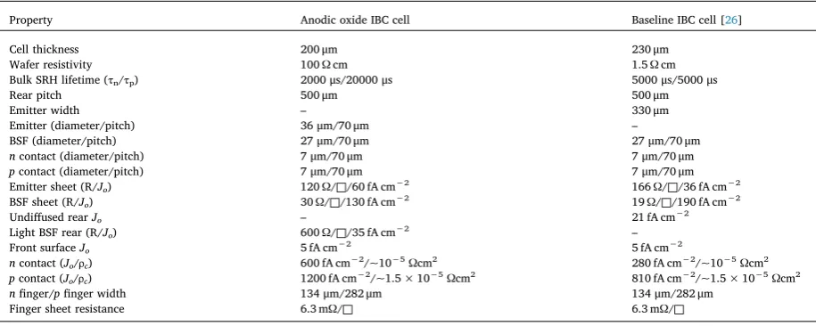
[image:7.595.69.527.319.502.2]Our 3D device simulations were carried out using Quokka 2 [40].Table A1lists the key cell parameters used in these simulations, which have been determined from the device itself, or from monitor wafers co-processed through each of the relevant process steps.
Table A.1
Key properties for the 2 × 2 cm2baseline and anodic oxide passivated IBC solar cells used in our 3D device modelling.
Property Anodic oxide IBC cell Baseline IBC cell [26]
Cell thickness 200 μm 230 μm
Wafer resistivity 100 Ω cm 1.5 Ω cm
Bulk SRH lifetime (τn/τp) 2000 μs/20000 μs 5000 μs/5000 μs
Rear pitch 500 μm 500 μm
Emitter width – 330 μm
Emitter (diameter/pitch) 36 μm/70 μm –
BSF (diameter/pitch) 27 μm/70 μm 27 μm/70 μm
ncontact (diameter/pitch) 7 μm/70 μm 7 μm/70 μm
pcontact (diameter/pitch) 7 μm/70 μm 7 μm/70 μm
Emitter sheet (R/Jo) 120 Ω/□/60 fA cm−2 166 Ω/□/36 fA cm−2
BSF sheet (R/Jo) 30 Ω/□/130 fA cm−2 19 Ω/□/190 fA cm−2
Undiffused rearJo – 21 fA cm−2
Light BSF rear (R/Jo) 600 Ω/□/35 fA cm−2 –
Front surfaceJo 5 fA cm−2 5 fA cm−2
ncontact (Jo/ρc) 600 fA cm−2/~10−5Ωcm2 280 fA cm−2/~10−5Ωcm2
pcontact (Jo/ρc) 1200 fA cm−2/~1.5 × 10−5Ωcm2 810 fA cm−2/~1.5 × 10−5Ωcm2
nfinger/pfinger width 134 μm/282 μm 134 μm/282 μm
Finger sheet resistance 6.3 mΩ/□ 6.3 mΩ/□
For the purpose of our simulations, we have neglected edge recombination and therefore all the simulated parameters will be slightly higher than if edge recombination were included.
Declarations of interests
None.
References
[1] S.W. Glunz, A.B. Sproul, W. Warta, W. Wettling, Injection-level dependent re-combination velocities at the Si−SiO2interface for various dopant concentrations,
J. Appl. Phys. 75 (1994) 1611–1614.
[2] M.J. Kerr, A. Cuevas, Very low bulk and surface recombination in oxidized silicon wafers, Semicond. Sci. Technol. 17 (2002) 35–38.
[3] K.R. Williams, K. Gupta, M. Wasilik, Etch rates for micromachining processing-Part II, J. Microelectromech. Syst. 12 (2003) 761–778.
[4] E.H. Nicollian, J.R. Brews, MOS Physics and Technology, John Wiley & Sons, 1982. [5] S. Pingel, O. Frank, M. Winkler, S. Daryan, T. Geipel, H. Hoehne, J. Berghold,
Potential induced degradation of solar cells and panels, Presented at the 35thIEEE
Photovoltaic Specialists Conference, (PVSC), 2010.
[6] S.W. Glunz, F. Feldmann, SiO2surface passivation layers – a key technology for
silicon solar cells, Sol. Energy Mater. Sol. Cells 185 (2018) 260–269.
[7] N.E. Grant, K.R. McIntosh, A review on low temperature chemically formed silicon dioxide for solar cell applications, Presented at the 48thAnnual Conference of the,
Australian Solar Energy Society, Canberra, Australia, 2010.
[8] J. Tong, S. Lim, A. Lennon, Tunnel oxides formed by field-induced anodisation for passivated contacts of silicon solar cells, Coatings 8 (2018) 81.
[9] N. Grant, K.R. McIntosh, Low surface recombination velocity on (100) silicon by electrochemically grown silicon dioxide annealed at low temperature, IEEE Electron. Device Lett. 31 (2010) 1002–1004.
[10] X.G. Zhang, Electrochemistry of Silicon and its Oxide, Kluwer Academic Publishers, 2001.
[11] P.F. Schmidt, W. Michel, Anodic formation of oxide films on silicon, J. Electrochem. Soc. 104 (1957) 230–236.
[12] N.E. Grant, K.R. McIntosh, Silicon surface passivation by anodic oxidation annealed at 400°C, J. Solid State Sci. Technol. 3 (2014) P13–P16.
[13] N.E. Grant, K.R. McIntosh, Low surface recombination velocities achieved by silicon dioxide grown electrochemically in nitric acid, Presented at the 37thIEEE
Photovoltaic Specialists Conference, 2011.
[14] W. Füssel, M. Schmidt, H. Angermann, G. Mende, H. Flietner, Defects at the Si/SiO2
[23] K. Ghowsi, R.J. Gale, Theoretical model of the anodic oxidation growth kinetics of Si at constant voltage, J. Electrochem. Soc. 136 (1989) 867–871.
[24] N.E. Grant, Surface Passivation and Characterisation of Crystalline Silicon by Wet Chemical Treatments, (2012) PhD Thesis.
[25] A.J. Bard, A.B. Bocarsly, F.F. Fan, E.G. Walton, M.S. Wrighton, The concept of Fermi level pinning at semiconductor/liquid junctions. Consequences for energy conver-sion efficiency and selection of useful solution redox couples in solar devices, J. Am. Chem. Soc. 102 (1980) 3671–3677.
[26] E. Franklin, K. Fong, K.R. McIntosh, A. Fell, A. Blakers, T. Kho, D. Walter, D. Wang, N. Zin, M. Stocks, E. Wang, N. Grant, Y. Wan, Y. Yang, X. Zhang, Z. Feng, P.J. Verlinden, Design, fabrication and characterisation of a 24.4% efficient inter-digitated back contact solar cell, Prog. Photovolt. Res. Appl. 24 (2016) 411–427. [27] D.E. Kane, R.M. Swanson, Measurement of the emitter saturation current by a
contactless photoconductivity decay method, Presented at the 18thIEEE
float-zone silicon, Phys. Status Solidi Rapid Res. Lett. 10 (2016) 443–447. [36] N.E. Grant, V.P. Markevich, J. Mullins, A.R. Peaker, F. Rougieux, D. Macdonald,
J.D. Murphy, Permanent annihilation of thermally activated defects which limit the lifetime of float-zone silicon, Phys. Status Solidi A 213 (2016) 2844–2849. [37] T. Rahman, A. To, M.E. Pollard, N.E. Grant, J. Colwell, D.N.R. Payne, J.D. Murphy,
D.M. Bagnall, B. Hoex, S.A. Boden, Minimising bulk lifetime degradation during the processing of interdigitated back contact silicon solar cells, Prog. Photovolt. Res. Appl. 26 (2018) 38–47.
[38] M.D. Abbott, K.R. McIntosh, B.A. Sudbury, Optical loss analysis of PV modules, Proc. 32nd EU PVSEC, Munich, 2016, pp. 976–979.
[39] www.pvlighthouse.com.au, Accessed date: 2 May 2019.