This work was supported in
Simulation and Experiments of a W -Band
Extended Interaction Oscillator Based on
a Pseudospark-Sourced Electron Beam
Yong Yin, Wenlong He, Liang Zhang, Huabi Yin, Craig W. Robertson, and Adrian W. Cross
Abstract— This paper presents the first experimental results
of an extended interaction oscillator (EIO) based on a pseudospark-sourced electron beam, which produced a peak output power over 38 W at W -band. The advantages of the newly developed device are: 1) transport of the electron beam by the positive-ion focusing channel without the need of an external magnetic field and 2) high interaction impedance and high gain per unit length of the EIO circuit. The experimental results agree well with the 3-D particle-in-cell simulations.
Index Terms— Extended interaction oscillator (EIO), pseudospark-sourced electron beam, vacuum electronics.
I. INTRODUCTION
P
SEUDOSPARK discharge systems based on the hollow cathode can produce axially symmetric-pulsed electron beams along the axis of the cathode cavity [1]–[3]. The production of higher current density electron beams, compared with thermionic cathodes, from pseudospark discharges has been convincingly demonstrated [4]. This property meets the urgent need of very high current density electron beams in the generation of coherent millimeter-wave and tera-hertz wave radiation.At millimeter and submillimeter wavelengths (terahertz frequencies), the achievable output power of the conventional O-type vacuum electronic devices is greatly limited by the electron beam current that can transport through the device at a particular voltage. The current density of a pseudospark-sourced electron beam is of the order of hundreds of A/cm2 or higher [5], [6], which enables a wide range of applications in generating millimeter-wave and submillimeter-wave radiation [7]. Yin et al. [8] demonstrated that the electron beam pulses with a 3-mm diameter can
part by the Engineering and Physical Sciences Research Council, U.K. under Grant EP/G011087/1 and in part by the National Natural Science Foundation of China under Grant 61201011. The review of this paper was arranged by Editor M. Thumm. (Corresponding author: Yong Yin.)
Y. Yin is with the University of Electronic Science and Technology of China, Chengdu 610054, China (e-mail: [email protected]).
W. He, L. Zhang, H. Yin, C. W. Robertson, and A. W. Cross are with the Department of Physics, University of Strathclyde, Glasgow G4 0NG, U.K. (e-mail: [email protected]; [email protected]; [email protected]; [email protected]; [email protected]).
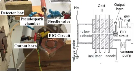
Fig. 1. Experimental setup of the W -band EIO based on a pseudospark-sourced electron beam and the schematic drawing of the experiment.
be transported distances up to 20 cm without a guiding magnetic field. To work with the pseudospark-sourced pulsed electron beam, automatic optimization techniques can be used to shorten the klystron interaction structure [9]. An alternative technique is to use the extended interaction oscillator (EIO) circuit, which has the advantages of high interaction impedance and high gain per unit length [10].
A W -band (75–110 GHz) EIO circuit operated in the 2π mode was selected for our first experiment because of its shorter interaction length as compared with a backward wave oscillator. The beam voltage was designed to be centered at 30.5 kV, which is suitable for a four-gap pseudospark dis-charge. This newly developed device combines the merit of a short interaction circuit in the EIO and the high current density property of the pseudospark-sourced electron beam to generate W -band coherent radiation. The design and optimization of the W -band EIO with a pseudospark-sourced electron beam has been carried out. Experimental results show that with a 35-kV discharge voltage, the oscillator produced W -band microwave radiation pulses with a 38-W peak power and 20-ns duration, which agrees well with the 3-D particle-in-cell (PIC) simulations using MAGIC.
[image:1.612.320.554.204.331.2]Fig. 2. Layout of the EIO circuit.
Fig. 3. Dispersion curve of the EIO circuit.
electron beam. It provides a compact and affordable way to generate tens of watts in W -band.
II. CIRCUITDESIGN ANDFABRICATION A. Circuit Design
The EIO operates at the 2π mode, and the number of the slots was optimized to achieve efficient circuit impedance. The layout of the EIO circuit is shown in Fig. 2. The circuit consists of identical nine-slot slow-wave structures that are strongly coupled by coupling cavities on both sides. The two coupling cavities (up and down) form the extended resonant cavity of the EIO circuit. The power is extracted out through a standard WR-10 waveguide attached to one of the cavities through circular apertures sized to provide the optimum Qe, which defines the ratio between the stored energy in the cavity at stable resonant conditions and the output power (with a perfect matched load) in one period. A 0.5-mm diameter beam tunnel passes through the center of the slots and intersects with the slow-wave structure. The total length of this circuit is 10 mm, and there is no external magnetic field.
The dispersion curve of the EIO circuit, in synchronism with a 30.5-kV beam, is shown in Fig. 3 (solid line). The velocity of the electron beam (or the beam energy) was chosen, so that the time interval of the electron travels from one slot to the adjacent slot is equal to the period of the electromagnetic wave supported by the slow-wave structure, therefore ensuring an efficient interaction between the beam and the interaction circuit.
[image:2.612.314.559.63.184.2]Through optimizing the dimensions of the coupling cav-ity, slot, and coupling hole, the maximum interaction impedance (R/Q) of 41.6 was achieved. The voltage dif-ference between the undesirable modes (2π +1 mode) and
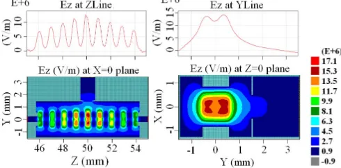
Fig. 4. Contour plots of the electric field component Ez at x = 0 and z=0 planes, and the field strength along the z- and y-directions.
(2π −1 mode) was maximized to about 6.3 kV, as shown in Fig. 3. The frequencies of the 2π and 2π−1 modes are 93.8 and 94.6 GHz, respectively.
B. PIC Simulation
The PIC codes MAGIC 3-D [12] and CST Particle Studio [13] were used to investigate the behavior of the EIO and to optimize its performance. In the simulations, a dc beam with 30.5-keV energy was injected into the interaction circuit. The beam diameter was 0.5 mm, and the current density was assumed to be ∼500 A/cm2 giving a total beam current of 950 mA. An axial magnetic field of 0.4 T was applied for beam focusing. When the beam–wave synchronous condition is satisfied, our simulation showed that the oscillation could build up and power be extracted out from the output structure. The oscillation could become stable about 11 ns after the beam was injected into the circuit. A contour plot of the electric field component Ez at the x = 0 and z =0 planes, and the electric field strength along the z- and y-directions are shown in Fig. 4. The top two diagrams in Fig. 4 show the electric field strength along the axis of the beam tunnel (z-direction) and along the center of the output waveguide (y-direction). The strong field in the center slot allows the 2π mode to have sufficient coupling to the output waveguide located in the center of the upper coupling cavity. The electric field strength ratio between the center slot and the others can be adjusted by changing the length of the coupling cavity.
[image:2.612.62.289.193.323.2]Fig. 5. (a) Phase space of the electrons. (b) Beam trajectory in the zy plane.
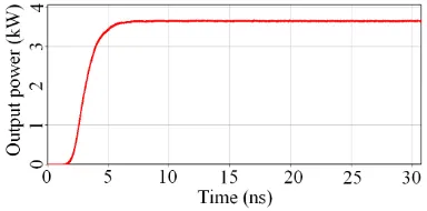
Fig. 6. Time-dependent output power at the output waveguide.
Fig. 7. Output power and oscillation startup time versus the beam voltage.
interaction efficiency as well as the output power dramatically. With the decrease in the voltage, the change in the operating mode from 2π to 2π+1 mode would also cause the output power to become zero at 27 kV. The simulated operating voltage region of the 2π mode in this EIO is 5.5 kV, which is in excellent agreement with what was estimated from the dispersion curve (6.3 kV).
[image:3.612.320.553.219.411.2]The electron beam from the pseudospark discharge is usu-ally very stable, especiusu-ally when no beam–wave interaction exists in the system and the working gas was fed into the system from the anode side at a very slow rate (∼1 mtorr/s). A typical electron beam pulse measured immediately after the anode, which had an aperture diameter of 0.6 mm, is
Fig. 8. Temporal evolution of the electron beam produced from a four-gap pseudospark discharge.
Fig. 9. (a) Beam voltage and (b) output power as a function of time.
shown in Fig. 8. From this measurement, it was estimated that the beam current at the beginning of the interaction region was 950 mA.
To reduce the complexity of the simulation, a stable beam current and a time-varying beam voltage, as shown in Fig. 9(a), were used to simulate the beam–wave interaction in the EIO circuit [14]. To reduce the computation time, the self-focusing of the beam in the ion channel was not included in the simulation, as well as the plasma generated by the pseudospark discharge. Instead, an axial magnetic field of 0.4 T was applied to guide the electron beam. Typically, for the full discharge process, it takes∼30–100 ns when the voltage changed from the applied 34 to 0 kV. The voltage change rate was∼1 kV/ns and can be varied by adjusting the capacitance of the external capacitor Cext used to maintain the discharge. When the voltage of the pseudospark beam changed from 34 to 0 kV in 100 ns, an output power of 5.6 kW with a full-width at half-maximum of 20 ns was predicted from the simulation and is shown in Fig. 9(b). The time duration that output power is generated is dependent on the voltage range of the EIO.
C. Fabrication and Cold Test
[image:3.612.78.270.300.395.2] [image:3.612.76.275.436.548.2]Fig. 10. Left: three parts of the circuit. Right: assembled EIO circuit.
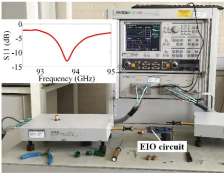
Fig. 11. Millimeter-wave measurement setup and measurement result.
cavities with and without the output structure were manu-factured by a computer numerical control machine at the University of Strathclyde. The slow-wave structure was manu-factured by wire erosion technology. The three parts were then connected together to form the EIO circuit with millimeter-wave measurements carried out using an Anritsu ME7808B (75–110 GHz) vector network analyzer (VNA). A photograph of the millimeter-wave measurement setup and the measured S11 parameters is shown in Fig. 11. The center frequency of the circuit is 93.8 GHz, and the 3-dB bandwidth is 275 MHz. The VNA millimeter-wave measurement result agrees well with the CST MWS simulations when assuming the effective conductivity of the copper to be 75% of the ideal value (5.8×10⁷S/m). The beam tunnel is in the middle of the slow-wave structure; therefore, its alignment tolerance is determined by the manufacturing process that avoids further assembly tolerance.
[image:4.612.63.282.225.394.2]III. EXPERIMENTALRESULTS ANDANALYSIS Experimental measurement of the W -band EIO based on the pseudospark-sourced electron beam was carried out at the University of Strathclyde. A four-gap pseudospark discharge chamber, which can hold off a discharge voltage up to 40 kV, was used. The discharge voltage swept from 38 to 25 kV to achieve the maximum output power. Two W -band horns, one for the output from the EIO and the second horn for the
Fig. 12. Typical test results of the voltage and the microwave pulse.
microwave detector, were used. The two horns are positioned at a distance of 20 cm. The microwave radiation pulse was measured by a W -band crystal detector. A typical measure-ment of the voltage and the microwave signal are shown in Fig. 12. The duration of the microwave waveform agrees well with the simulation result, as shown in Fig. 9(b).
To estimate the radiation power, the crystal detector was calibrated twice using a 1.5-W, 90–97-GHz solid-state source. First, the detector was connected to the solid-state source through an attenuator to measure the response curve at differ-ent input powers. The other calibration used dual horns with a separation distance of 20 mm (the same distance used in the EIO experiment). One horn was connected to the solid-state source, and the other was connected with the crystal detector. The response of the detector at different output powers was recorded. From the calibration data, the direct ratio of the radiation power to the amplitude of the crystal detector was obtained. The peak power of the radiation was found to be ∼38 W. The output frequency was examined using a high-pass waveguide cutoff filter, which operated above 92 GHz. The radiation frequency was found to be above 92 GHz, which also coincides with the VNA millimeter-wave measurement result of 93.8 GHz.
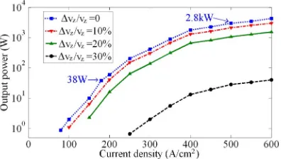
Fig. 13. Relation between the current density to the output power and the axial velocity spread.
the interaction efficiency adversely due to reduced overall synchronism between the beam and the wave. Fig. 13 shows that the combined effects from the axial velocity spread and beam loss in the interaction are possible reasons of reduced output power in the experiment. Future experiments will add an inline beam diagnostic at the end of the interaction region to measure the beam current at the end of the interaction region. This would give more accurate information on the velocity spread of the beam.
IV. CONCLUSION ANDDISCUSSION
The pseudospark-sourced electron beam, which is self-focused by the positive-ion channel generated from the pseudospark discharge process, was successfully used to drive a W -band EIO circuit to generate coherent radiation. The back-ground unmagnetized plasma can be considered as a dielectric media with a dielectric constant of εr =1−ω2pe/ω2. As the operating frequency is far away from the plasma frequency, the plasma would have negligible effect on the output power of the EIO. However, the plasma would upshift the output frequency slightly, and from the dispersion equation, it is ∼10%. The measurement of the exact frequency with a mixer is scheduled for a future experiment.
There are two possible ways to increase the output power of this device. The first one to use a beam voltage with slower decrease, this will allow more electrons to be located in the oscillating voltage range over relatively longer time, thus increasing the output power of the device. In the pseudospark discharge, the discharge duration can be adjusted by using different external capacitances. The second way is to minimize the energy spread of the pseudospark-sourced electron beam, such as using the postacceleration technique [4] which can reduce the axial velocity spread of the pseudospark-sourced electron beam to ∼5%.
This experiment demonstrates an original type of com-pact and affordable radiation source for the genera-tion of millimeter-wave and submillimeter-wave radiagenera-tion.
The pseudospark-sourced electron beam has higher current density than a thermionic electron beam, and the beam for-mation and focusing does not require an external magnetic field. It is an excellent affordable, compact, and robust pulsed electron beam source to drive an EIO circuit operating at higher frequencies with reasonably high radiation power.
ACKNOWLEDGMENT
The authors would like to thank D. Barclay for the help in manufacturing and assembling the circuit.
REFERENCES
[1] M. A. Gundersen and G. Schaefer, Physics and Applications of Pseudosparks (NATO ASI Series), vol. 219. New York, NY, USA: Plenum, 1990, pp. 55–76.
[2] K. Frank and J. Christiansen, “The fundamentals of the pseudospark and its applications,” IEEE Trans. Plasma Sci., vol. 17, no. 5, pp. 748–753, Oct. 1989.
[3] S. Muhl and A. Pérez, “The use of hollow cathodes in deposition processes: A critical review,” Thin Solid Films, vol. 579, pp. 174–198, Mar. 2015.
[4] H. Yin, A. W. Cross, A. D. R. Phelps, D. Zhu, W. He, and K. Ronald, “Propagation and post-acceleration of a pseudospark-sourced electron beam,” J. Appl. Phys., vol. 91, no. 8, pp. 5419–5422, Apr. 2002. [5] D. Bowes et al., “Visualization of a pseudospark-sourced electron beam,”
IEEE Trans. Plasma Sci., vol. 42, no. 10, pp. 2826–2827, Oct. 2014. [6] D. Bowes et al., “X-ray emission as a diagnostic from
pseudospark-sourced electron beams,” Nucl. Instrum. Methods Phys. Res. B, Beam Interactions Mater. Atoms, vol. 335, pp. 74–77, Sep. 2014.
[7] A. W. Cross, H. Yin, W. He, K. Ronald, A. D. R. Phelps, and L. C. Pitchford, “Generation and application of pseudospark-sourced electron beams,” J. Phys. D, Appl. Phys., vol. 40, no. 7, pp. 1953–1956, Jul. 2007.
[8] H. Yin et al., “Millimeter wave generation from a pseudospark-sourced electron beam,” Phys. Plasmas, vol. 16, no. 6, p. 063105, Jun. 2009. [9] C. J. Lingwood, G. Burt, K. J. Gunn, R. G. Carter, R. Marchesin, and
E. Jensen, “Automatic optimization of a klystron interaction structure,” IEEE Trans. Electron Devices, vol. 60, no. 8, pp. 2671–2676, Aug. 2013. [10] J. P. Pasour et al., “Demonstration of a multikilowatt, solenoidally focused sheet beam amplifier at 94 GHz,” IEEE Trans. Electron Devices, vol. 61, no. 6, pp. 1630–1636, Jun. 2014.
[11] A. E. Dubinov, I. L. L’vov, S. A. Sadovoy, V. D. Selemir, D. V. Vyalykh, and V. S. Zhdanov, “Ultraminiature pulsed periodic generator of power-ful microwave pulses, based on gas discharge in hollow cathode,” IEEE Trans. Plasma Sci., vol. 40, no. 8, pp. 2079–2082, Aug. 2012. [12] B. Goplen, L. Ludeking, D. Smith, and G. Warren, “User-configurable
MAGIC for electromagnetic PIC calculations,” Comput. Phys. Commun., vol. 87, nos. 1–2, pp. 54–86, May 1995.
[13] CST-Computer Simulation Technology. [Online]. Available: https://www.cst.com/Products/CSTPS, accessed Aug. 2015.