Rochester Institute of Technology
RIT Scholar Works
Theses
Thesis/Dissertation Collections
1999
Process development and reliability of thin gate
oxides
Keith Capasso
Follow this and additional works at:
http://scholarworks.rit.edu/theses
This Thesis is brought to you for free and open access by the Thesis/Dissertation Collections at RIT Scholar Works. It has been accepted for inclusion
in Theses by an authorized administrator of RIT Scholar Works. For more information, please contact
Recommended Citation
PROCESS DEVELOPMENT AND RELIABILITY
OF THIN GATE OXIDES
by
Keith
C.
Capasso
A Thesis Submitted in Partial Fulfillment
of the Requirements for the Degree of
~STERSof
SCIENCE
10
MICROELECTRONICS MANUFACTURING ENGINEERING
Approved by:
Dr. Michael A. Jackson
(thesis
advisor)
Dr. Santosh Kurinec
(COmmittee member)
Mr.
Karl Hirschman
(committee member)
Dr. Lynn F. Fuller
(Department Head)
Microelectronic Engineering
College of Engineering
Rochester Institute of Technology
ACKNOWLEDGMENTS
I
wouldlike
to thankDr. Michael
Jackson,
Dr. Santosh
Kurinec,
Dr.
Turkman,
andKarl
Hirschman for
theirsupport andsuggestionsduring
thiswork.I
would alsolike
to recognizeDr. Fuller
and theMicroelectronic Department
for
access toprocessing
equipment and materials.Special
thanks gotoScott
Blondell,
Dave
Yackoff,
andRich Battaglia
for
keeping
theequipmentTABLE OF CONTENTS
Section
Page
List
ofFigures
ix
List
ofTables
xivList
ofSymbols
xviAbstract
xviiiChapter
I
Introduction
1
Chapter II
Background
3
2.1
Silicon
Dioxide Physical Structure
4
2.2
Si-Si02
Interface
6
2.3
Bulk
Oxide Charge
9
2.4
Carrier Injection into Oxide Film
12
2.4. 1
Channel Hot Electrons
(CHE)
12
2.4.2
Drain Avalanche Hot Carriers
(DAHC)
13
2.4.3
Fowler-Nordheim
(FN)
Tunneling
13
2.4.4
Direct
Tunneling
15
2.5
Oxynitrides
asGate Dielectrics
17
2.6
Properties
ofOxynitrides
20
2.6.1
Oxidation Rate
21
2.6.2
Infrared Measurements
22
2.6.3
Interface Measurements
26
2.6.4
Tunneling
andLeakage Current
28
2.7. 1
Thermal Nitridation
withNH3
33
2.7.2
Thermal
Nitridation
withN20
35
2.7.3
Nitridation
by
Plasma-Assisted
Processing
35
2.7.4
Nitrogen Implantation
(into
substrate)"A
Time
Line"
43
2.7.5
Reliability
ofNitrogen Implantation Methods
48
2.7.6
Implanting
into
thePoly
Gate
49
2.7.7
Nitrogen Implantation Work Done
atRJT
56
2.8
Processing
Issues
57
2.8.1
Surface
Roughness
58
2.8.2
Metal Contamination
59
2.8.3
Dopant Penetration
60
2.8.4
Plasma Induced Damage
63
Chapter m
Testing
Methods
70
3.1
Testing
Methods
70
3.2
Time-to-Dielectric Breakdown
(TDDB)
73
3.3
Charge-to-Breakdown
(Qbd)
74
3.4
Surface Charge Analysis
(SCA)
75
3.5
Reliability
Tools
77
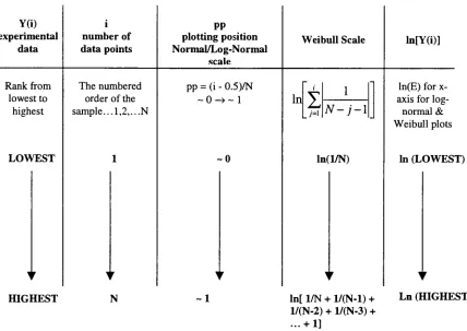
3.5.1
Cumulative Distribution Function
77
3.5.2
Log
Normal Cumulative
Distribution
Function
78
3.5.3
Weibull Cumulative Distribution Function
79
Chapter IV
Experiment
82
4.1.1
RUN A
85
4.1.2
RUNB
85
4.1.3
RUNC
85
4.1.4
RUND
86
4. 1
.5Sputttered
vs.Evaporated Aluminum Gate
86
4.1.6
RUNAR-1
87
4.2
Gate Oxide DOE
87
4.2.1
Processing
Information
88
4.2.2
Experimental
Setup
89
4.2.3
Noise Reduction
90
4.3
PHASE 2: N-implanted RUN
92
4.3.1
Fowler-Nordheim
(FN)
Study
92
4.3.2
Charge-to-Breakdown
(Qbd)
Study
93
4.3.3
Time-to-Breakdown
(TDDB)
Study
94
4.3.4
Weibull Analysis
95
4.3.4
Capacitance-Voltage
(CV)
Analysis
97
4.4
PHASE 3:
Poly
gateMOS-C Implementation
100
4.4.1
Initial Run
RUN LP
A-1
105
4.4.2
Nitrided /
Self-Aligned
Poly
RUN
1 05
Chapter V
Results
109
5.1
Thin Oxide Characterization
109
5.2
DOE
for
Optimizing
Thin
Oxide Recipe
1 12
5.2.2
DOE Conclusion
121
5.3
FN-tunneling
122
5.4
Charge-to-Breakdown
126
5.5
Time-to-Breakdown
(TDDB)
128
5.6
N-implanted
aluminumgateMOS-C
128
5.7
Weibull Analysis
ofN-implanted Samples
133
5.8
C-V Analysis
135
5.9
Poly-Si
Gate Dielectric
136
Chapter VI
Conclusions
140
References
142
Appendix A:
Standard
flat-field,
aluminum-gateMOS-C
processflow
APP-1
Appendix
B:
LOCOS,
polysilicon-gateMOS-C
processflow
APP-7
Appendix C:
Sorted FN
characteristicsfor
oxidizedsamplesAPP-1
8
Appendix D: Breakdown
resultsLIST OF FIGURES
Figure
Page
1
Basic Structural Unit
ofSilicon Dioxide
4
2
Fused Silica Polyhedra Network
5
3
Si-0 Material Film Structure
5
4
Origin
ofInterface
andSurface Traps
7
5
Electron
Trapping by Dangling
Bond
8
6
Hole
Trapping by
Hydrogen Terminator Site
andStretched Bond
8
7
Depassivation
ofH-terminated
Bonds
9
8
Various Forms
ofCharge
10
9
Deal Triangle
-Model
ofFixed Charge
1 1
10
Energy Bandgap
Diagram for FN
Tunneling
in
aMOSFET Gate Oxide
14
11
Oxide Band Diagram
Showing
thePresence
of aCentroid
15
12
Band diagram showing direct
tunneling
16
13
FN
tunneling
I-V
curves ofAl-gate
n-channelMOS
structures16
14
Barrier Height
for Silicon Nitride Dielectric
andONO Stack Dielectric
17
1
5
Bombardment
oftheInterface
by
Channel Hot Electrons
1 9
16
OxNy
Ternary
Diagram
21
17
ERD Spectrum
of40nm
Si3N4
Oxidized for
4 hours in
H20/02
22
1 8
JR Spectra
(
1
300
-600
/cm)
as aFunction
oftheSiOxNy
Nature
23
19
FTIR Spectra
ofSamples Deposited
withSeveral Flow Ratios
24
20
Deconvolutioninto Gaussians
ofther=200Sample Spectrum
25
23
I-V
Characteristics
ofAu-Si3N4-Si
diode
atRoom Temperature
29
24
Conduction
Band Barrier Heights & Dielectric Constants
ofOxynitrides
30
25
Leakage Current
Density
of~2.0nmDielectrics
3 1
26
Leakage Current
Density
of~3.0nmDielectrics
3 1
27
Relationship
between
tunneling
currentanddielectric film
composition32
28
SIMS Data
onNitride Interface
asaFunction
ofSiN"
Ions
36
29
SIMS Data
onNitride Interfaces
as aFunction
ofNitridation Time
37
30
Normalized Plots
ofIntegrated Ion Counts
vs.Time
for
SiN"Ions
38
3 1
Normalized Plots
ofIntegrated Ion Counts
vs.Time for
CsN1"
Ions
39
32
J-V
Characteristics
-NMOS-C,
~5nmthick
Oxide,
Al-gate Electrodes
40
33
J-V for
~2& 3nm
Oxide,
for Non-nitrided & Fully-Nitrided Interfaces
41
34
Implantation into Poly-Si Gate
ofMOS Capacitor
50
35
MOSFET Effective Electron & Hole
Mobility
for Various Oxide Films
53
36
Threshold Voltage Shifts With
andWithout Nitrogen Implant
54
37
Nitridation
-Gate Voltage Shift Under
Constant-Current
Injection
54
38
Constant Current TDDB With
andWithout Nitrogen Implantation
55
39
Field Oxide Edge
Thinning
oftheGate Oxide
59
40
P+Doped Polysilicon Gate
Degradation
due
toBoron Penetration
61
41
Qbd
-Thermal Gate Oxides
with
Different Amounts
ofBoron
61
42
Effect
ofBoron
Penetration in N20
Nitrided
Oxide
62
43
Qbd
-Comparison for Thermal
and
N20-Annealed
Gate
Oxides
63
44
Topography
Dependent
Charging
(TDC)
65
46
How RIE
Lag
Increases Size
ofAntenna
& Subsequent Damage
66
47
Example
ofHow
AntennaRatio Increases Oxide Current
67
48
Effects
ofU
onQBD
for PMOS
Damaged68
49
Charge-to-Breakdown Values
as aFunction
ofCell Position
69
50
Si02
Energy
Band Diagram
Showing
Trapped Holes
andElectrons
7 1
5 1
Ramped Voltage Stress Test
Setup
72
52
Failure Modes for Dielectric Breakdown
72
53
Constant Voltage TDDB Stress Test
Setup
73
54
Charge-to-Breakdown Stress Test
Setup
74
55
A SEM Photograph
ofTwo Breakdown Spots
75
56
Surface Charge Analyzer
(SCA)
Test
Setup
76
57
Example
of aCumulative Distribution
78
58
Example
ofaWeibull Distribution
8 1
59
Standard MOS
Capacitor Process Flow Diagram
83
60
Flowchart
ofProcessing
Steps Needed
toComplete
aRun
9 1
61
Charge-to-Breakdown
vs.Injected
Current
Density
94
62
Example
of aNormal Distribution
96
63
Example
ofaLog-Normal Distribution
96
64
Capacitance-Voltage
PAR
model4 10
system97
65
Cox
vs.Gate Area
for
Theoretical
andExperimental Data
98
66
Cmin
vs.Gate Area for Theoretical
andExperimental Data
98
67
Equivalent MOS
capacitorcircuit modelswithseries resistance99
69
Reticle showing
gateareasfor fabricated MOS-C
104
70
Self-Aligned (S
A)
Poly-Gate MOS Capacitor Process Flow Diagram
1 06
7 1
Cumulative Dielectric
BreakdownPlot
ofanEarly
Oxidation Run
109
72
Breakdown Plot
Effects
ofPlasma
Processing
ontheAl-gate MOS-C
1 1 1
73
Breakdown Plot for Oxidation Processed
withArgon Ambient
112
74
Prediction Plot for
Qox
for
Changing
Temperature
andAnneal
1 1
6
75
Prediction Plot for
Nsc
for
Changing
Temperature
andAnneal
119
76
Cumulative Dielectric Breakdown for
theMultiple
Runs in
theDOE
121
77
FN Plot
of an-80AOxide Film
whereN
wasused as theInert Ambient
122
78
FN Plot
of an~80AOxide Film
whereAr
wasused as theInert Ambient
122
79
FN Plot
ofan -80A Oxide Film
whereN
was usedastheInert Ambient
124
80
FN Plot
of an-122AOxide Film
whereN
was usedastheInert Ambient
124
8 1
FN Plot
of an-1
92A
Oxide Film
whereN
was usedasthe
Inert Ambient
1 25
82
FN Plot
of an-214AOxide Film
whereN
wasusedastheInert Ambient
125
83
Oxidation Kinetics for N-implanted Samples
atRJT
129
84
Cumulative Dielectric Breakdown
from
theInitial N-implanted Run
129
85
Breakdown
Comparison b/n N-implanted & Non-implanted
at~80A130
86
Breakdown Comparison b/n
N-implanted
& Non-implanted
at~1
20A
131
87
Breakdown
b/n N-implanted & Non-implanted
at-150A-190A
132
88
Breakdown
vs.Oxide Thickness for N-implanted & Non-implanted
133
89
Weibull
Plot
Breakdown
ofN-implanted
Samples
from
theInitial Run
134
90
Log-NormalPlot
-Breakdown
of
N-implanted from
theInitial Run
134
92
Breakdown for Poly-Si Gate LOCOS
andRat Field MOS-C Devices
1 36
93
Breakdown
for N-implanted Poly-Si Gate LOCOS
andHat Field MOS-C
1
37
94
Breakdown
for
"Self-Aligned"LIST OF TABLES
Table
Page
1
Properties
ofPotential Dielectric Material
20
2
Lot Split Information
onSoleimani
et. al,DCE Research 1995
44
3
Implant Information
onSoleimani
etal.,DEC Research 1995
45
4
Lui
etal.Process Information
47
5
Lui
et al.Implant Information
47
6
Haddad
andLiang
Poly-implant
Methodology
50
7
Kuroi
et al.Process Split Information
(-100A)
52
8
Lopez
andKurinec RIT
Methodology
57
9
Sputter Settings for Al-gate MOS-C Run
86
10
Run Recipes for
theDesigned Experiment
90
1 1
Generation Table for
Plotting
Normal, Log-Normal,
andWeibull
95
12
Qox
Response Data
113
13
XsResponse Data
113
14
NSc
Response Data
113
15
Qox
ANOVA Components114
16
Qox
Coefficients
115
17
ts ANOVA Components
117
18
TS Coefficients
118
1 9
Nsc
ANOVA
Components
1 1 8
20
Nsc
Coefficients
119
22
Charge-to-Breakdown
(Qbd)
RUN 3 Results
127
23
Charge-to-Breakdown
(Qbd)
RUN 4 Results
127
LIST
OF SYMBOLS
BOE
Buffered Oxide Etch
CHE
Channel Hot Electrons
DI
De-ionized
waterDAHC
Drain Avalanche Hot Carriers
FN
Fowler Nordheim
Ci
Insulating
Capacitance
CV
Capacitance-Voltage
Dit
Density
ofInterface Traps
df
Degrees
ofFreedom
ec
Dielectric
Permittivity
eo
Permittivity
ofFree Space
Gm
Measured Conductance
HF
Hydrofluoric Acid
Id
Drain
Current
I/I
Ion Implant
J
Current
Density
k
Boltzmann Constant
kT
Thermal
Energy
LOCOS
Local
Oxidation
ofSilicon
LPCVD
LowPressure Chemical Vapor Deposition
MOSFET
Metal Oxide Semiconductor Field Effect Transistor
MOS-C
Metal Oxide Semiconductor Capacitor
Na
Sodium
Nsc
Substrate
Doping
<|>MS
Metal-Semiconductor
Work Function
q
Electronic Charge
(magnitude)
Qbd
Charge-to-Breakdown
Qf
Fixed Charge
QlND
Induced Charge
Qm
Mobile Charge
Qos
Oxide Surface Charge
Qot
Oxide Trapped Charge
Qox
Total Oxide Charge
r
Radius
RTE
Reactive
Ion Etch
SA
Self-Aligned
SCA
Surface Charge Analysis
Si
Silicon
SSres
Sum-of-SquaresResidual
SST
Sum-of-SquaresTotal
Si02
Silicon Dioxide
TCA
TriChloroEthaneTDDB
Time-to-DielectricBreakdown
tox
Oxide Thickness
14-8.85
xKT'F/cm
8.617
xlO"5eV/K0.0259
eV(T
=300K)
-19
1.6
x 10"1*ABSTRACT
The
Semiconductor
Industry
Association's(SIA)
currentNational
TechnologicalRoadmap
callsfor
thedevelopment
of a suitabledielectric
materialfor
usein
gate oxidefor
the0.18|im
generation of chips andbeyond.
Some
ofthekey
challengesidentified
are resistance tooxide trapped charge generation
from higher levels
oftunneling
currents and/or plasmaprocessing, and
formation
of an effectivebarrier
todopant
penetrationduring
the gateprocessing.
One promising
materialtomeetthesechallengesis
nitridedthermaloxide.Development
of agrowth process thatyieldshigh
quality,lOnm thick,
thermally
grownSi02
films
atRJT
for
use as a gatedielectric is described.
Thin
oxides(8nm
-20nm)
weregrown
by
thermal oxidationfollowed
by
inert
annealsin Ar
andN2.
Nitrided
oxides werecreated
by implanting
N2
(dose
range:5el3
-lei
5
/cm2)
into
the substrate prior to gateoxidation.
Test
equipment wassetup
tostudy Fowler Nordheim
(FN)
tunneling
anddielectric
breakdown.
Test
structures consisted of conventional and novelMOS
capacitor structures withaluminum and poly-silicon gate electrodes.
Scaling
RJT's
existing,20nm
oxidation process tolOnm
resultedin degradation
ofdielectric
strengthfrom
>lOMV/cm
to~6-7MV/cmfor Al-gate MOS
capacitors.Replacing
theAl
gate material with poly-silicon restored thedielectric
strength tolOMV/cm.
Performing
anN2
implant
through ascreening
oxide, prior to gate oxidation, wasinvestigated
as a means ofobtaining
a nitrided thermal oxide.For
certaindoses (5el3
-5el4
/cm2),
Al-gate MOS
capacitors exhibited an
improved dielectric
strength as the mean valueincreased from
6-7MV/cm
to ~9MV/cm.Poly-Si
gateMOS
capacitors showed a similarimprovement for
thenitrided oxides,
exhibiting
meandielectric
strength valuesin
the10-12MV/cm
range.Fowler-Nordheim
(FN)
tunnel current measurements showed that the nitridedfilms
exhibitlower
that a
12nm
nitrided oxide,for
a certaindose
(5el4/cm2),
exhibited equivalent electricalperformance toa
20nm
thermally
grownSi02
oxide.In
conclusion,a process wasdeveloped for
CHAPTER
I
INTRODUCTION
Each
year, theSemiconductor
Industry
Association
(SLA)
generates a guidelinefor
technological growth
in
the semiconductorindustry,
known
as theNational Technological
Roadmap.
It identifies
research needs and provides goalsfor
theindustry
to thrive.According
to the
1997
revision, the gatedielectric has been
recognized as one of the mostdifficult
challenges
for future device
scaling.Most
gatedielectrics
usedtoday
arehigh
quality,thermally
grown oxides.Continued
scaling
require that these oxidesbe
made thinner.Currently,
in
the0.25um
generation, theseoxidesare
only 40-50A
thick.For
future
generationsthey
are expectedto shrinkto:30-40A (for
0.1
8um),
20-30A (for
0.15u,m),
15-20A (for
O.lOum),
<15A(for
0.07um),
and <15A(for
0.05um).
A
problem existsin scaling
thesethermally
grown oxidesdue
toinherent
tunneling
currents.
The
shrinkage ofthesedielectrics
below
about15-20A
thicknessis
predictedtoresultin
tunneling
currents >lA/cm
.According
to the1997
Roadmap,
sincetunneling
currents willscale
exponentially
withfurther
thickness reductions,thermally
grown oxides willlikely
be
phased out pastthe
0. 10
|jmgeneration,whichis
expectedtobe in
productionnear2006.
The
Roadmap
Front-End
Processes
technology
working group has
issued
thefollowing
stability
andinterface
characteristics to serve as a gatedielectric.
Years
of research anddevelopment
are requiredtoidentify
andqualify
asuitable alternativematerial."1
The roadmap has identified
near-term gatedielectric
solutionsrequiring
thefabrication
and use of ultrathin siliconoxide, oxynitride
films,
or silicon nitridefilms.
However,
thesenearterm solutions will
impose
severe restraints on surface preparation, ambient control, contactmaterial
development,
and post process thermalbudgets.
Long
term solutions requireidentification
of materials with ahigher
dielectric
constant(k>20)
and other electricalcharacteristics
(i.e.
low
density
ofinterface)
andreliability
approaching
that ofhigh-quality
thermally
grown oxides.High-k dielectrics
musthave
abandgap
of4-5eV
with abarrier height
of >leV to
limit
thermionic emission andFowler-Nordheim
tunneling.In
addition, the newdielectric
material musthave
negligibletrap
densities
toinhibit Frenkle-Poole
tunneling.Finally,
the material musthave
excellentdiffusion barrier
properties to prevent gate materialcontamination ofthe transistorchannel.
The
scope of this work was todevelop
robust100A
thermally
grownSi02
films
andelectrically
characterize thesefilms
to establish process capability.One
of the near termdielectric
solutions proposedby
theroadmap
wasinvestigated
by implanting
nitrogeninto
substrates,
followed
by
thermal oxidation toform
an oxynitridefilm. Electrical
characterizationCHAPTER n
BACKGROUND
The framework for
thisproject canbe
summarizedin
the twostatementsbelow:
1
.In characterizing
gate oxides,thefollowing
criteriashouldbe
considered:the
dielectric
should matchdesign
specificationsthe
uniformity
across the wafer,from
wafer-to-wafer, run-to-run shouldbe
<
1%,
2%,
and3% respectively
charge
densities in
the oxide and at theinterface
shouldbe in
the5x10
-lxlOn/cm2
range
dielectric breakdown
strength shouldbe
>lOMV/cm,
implying
a pinholefree,
low
defect film
the
film
shouldexhibithigh
resistancetominority
carrierdamage
the
film
should exhibit resistancetodopant
penetration2.
Reliability
of the oxideis divided into
two categories:dielectric breakdown
andhot
carrier
injection degradation.
A
general overview oftheformation
and properties of gatedielectrics
is in
ordertoestablish the2,1
Silicon Dioxide Physical Structure:
Silicon
dioxide,
as usedin
semiconductor processing,is
alsoknown
as silica.The
structure ofsilicacan
be
found
in
crystalline, vitreous, and amorphousforms. The form found in
most gate
dielectrics
is
athermally
grown vitreous(a.k.a.
fused silica) form. Vitreous
silicahas
a short-range crystal structure withthe
basic
structural unit ofthermally
grown silicontaking
theform
ofSi04.
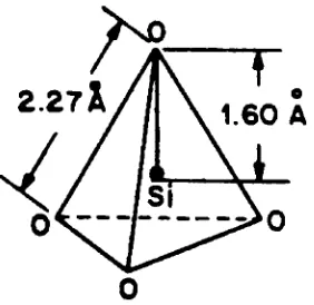
This
crystal consists offour
oxygen atomssitting
at the corners of a triangularpolyhedron.
In
the center ofthe polyhedronis
a single silicon atom.The
tetrahedraldistance
between
the silicon and oxygenions is
1.60A,
the oxygen-oxygenion distance is 2.27
A,
andthesilicon-silicon
distance is
3.12A.2Each
of thefour
oxygenions is covalently bonded
to the [image:24.565.203.344.359.496.2]silicon atom,
satisfying
the silicon valence shell.The
crystal celldescribed is illustrated in
Figure 1 below:
Figure 1: BasicStructuralUnitofSiliconDioxide.
[4]
The
polyhedra arejoined
toeach otherby
an oxygenion
called abridging
oxygen, whichis
sharedbetween
twotouching
polyhedra.Some
ofthe oxygenions
are non-bridging,bonded
to
only
one silicon atom.Thermally
grownSi02
consistsprimarily
of a random orientedQ
Bridgingoxygtn<> Nonbridgmgoxygan Silicon
INetworkmodifier
@) Hydroxyl group
Network termer
Figure 2: Fusedsilica polyhedra network.
[3]
The larger
theratioofbridging
tonon-bridging
sites, themore cohesive andless damage
prone the oxide
is.
The Si-O-Si bond
angleis approximately
144,
and canvary from 1
10 to180. When
compared to crystalline silica(quartz),
the vitreous stillhas
atendency
toform
acharacteristic six-silicon
ring.
However,
the vitreous structureis
much more open since silicondioxide
moleculesoccupy
only 43%
of the space.This
open structure of the vitreousform
explains the
lower
density
(2.2
g/cm3as compared to
2.65
g/cm3for
quartz) and the ease atwhich
impurities
can enter anddiffuse readily
through the oxidelayer.4
The
differences
canbe
seen
in Figure 3.
OXYGEN
SILIC
Atomicmovement
in
theoxideis
morelikely
to occurby
themovementofoxygen atomsrather than silicon atoms, since
4 Si-O bonds
mustbe broken
to release a silicon atom, whileonly 2 bonds
are requiredtofree
abridging
oxygenatom.If
thelatter
scissionoccurs, an oxygenvacancy,withanet positivecharge,
is
created.2.2
Si-SiOi
Interface:
One
of the mostimportant
aspects of thedielectric is
the transition regionfrom
thesubstrate to the
dielectric film.
The
characteristics,both electrically
and physically,play
animportant
rolein
the operation of thedielectric.
The interface is
the major source ofcharge-trapping
sites orenergy
statesin
theenergy band diagram. Each energy
stateis
associatedwith asingle atom atthe surface.
Any
charge carrierthatfills
one oftheseenergy
statesbecomes fixed
at the atom
it is
associated with.These
states are alsoknown
asinterface
traps sincethey
effectively
trap
free
carriers at the surface.The
physical origin oftheseenergy
stateshas
notbeen completely
established,but Deal's
experimental workindicates
thatsurface states originatefrom
unsatisfied,dangling
bonds
at the silicon surface and thedensity
of these states areorientation
dependant. Possible
sources ofenergy
states could arisefrom bonded foreign
atomsand crystal
defects
nearthesurface.Deal
proposes surface stateshave
thefollowing
properties:1
.)A
surface stateis
capable oftrapping
oremitting
a carrier.2.)
The energy levels
ofthese states arefound
withintheforbidden
gap.3.)
The
surface state canbe
either adonor
or acceptortype.Types
are characterizedby:
a)
A
monovalentdonor
trap
has
two charge states, +1 and0.
It
is
charged positive(+1)
b)
A
monovalent acceptortrap
has
two charge states,0
and -1.The
trap
is
neutral(0)
whenthe
trap
is
empty,andis
negative(-1)
whenit is full.
4.)
Interface
states are not associated with well-definedenergy levels
sincethey
aredue
to adisruption
oftheperiodicity
ofthecrystallattice.
With
theformation
of silicondioxide
at the surface, thesebonds
canbe
satisfied,ideally leaving
no surface states.
However,
it is
also possiblefor
the oxidation not to tieup
all thebonds,
leaving
a significant number ofenergy
states.Only
arelatively
small number of residualdangling
bonds is
required tosignificantly
alterdevice
performance.Figure 4 illustrates
thedangling
bond.
Danglingbond
(a)
(b)
Surface
SiO,
+
(C)
4
,if
(d)
Figure4:
(a) Dangling
bondsformedby
theabruptterminationofthesiliconlattice,(b)
AThese
sitestrap
negativechargeby
creating
acovalentbond.
Incomplete
silicapolyhedra wouldalso act as an
trap
asillustrated in Figure 5.
Figure 5: Electron
trapping
by dangling
bond(a)
offof oxygenatom,
(b)
off of silicon atom.[7]
A
trap
can alsobe
generatedfrom
weak or strainedbonds in
thelattice.
Weak bonds
arecommon at passivation sites where
hydrogen has
attachedtodangling
bonds
attheinterface. The
energy
ofthis passivationis
small and caneasily be broken.
Strained bonds
canbe
a result ofdefects like
oxygen vacancies.Both
types of traps areusually
positivehole
traps and areillustrated in Figure 6.
oxygen vacancy
(a)
(b)
Silanol,
aformation found in
theoxide,has
the potential tobecome
anegativetrap
site. Silanolis formed
whenhydrogen is introduced in
theoxidation process,from
sourceslike
moisture.The
hydrogen
bond
ofthe silanol canbe broken easily
by
ahydrogen
atom,resulting in
adangling
bond.
The hydrogen is
removedin
theform
of adiatomic
molecule thathas
the potential tofurther depassivate bonds. Figure 7 illustrates
this mechanismoftrap
formation.
O)
v<r(H)
(o:
Figure 7: Depassivationof aHterminatedbond.
[7]
=<H)
2.3
Bulk
Oxide Charge:
The
interface is
nottheonly
source of charge sites,as chargecan alsobe
found
withinthebulk
ofthe oxide.In
addition tointerface
charge(Qn),
thereis
alsofixed
charge(Qf),
mobilecharge
(Qm),
and oxide-trapped charge(Q0t). Examples
ofthese charges are shownin
theFigure
1
B
I I
"f0A
0
=
=
(2K5ft^KXs)
C
(o
_||
fl
{1
ff
-|.
1.|_
oxide-substrate
interface
0=0=0=0=0=0
Figure 8: Various FormsofCharge...
(A)
- Oxide Trapped Charge(Qot)
,(B)
- Mobile Ionic
Charge
(Qm), (C)
Interface Charge(Qit), (D)
- Fixed Charge (Qf).[7]
Fixed
charge(Qf)
is located
within35A
oftheSi/Si02
interface,
in
the transitionregion.The
chargemay be due
to trivalent silicon centers,non-bridging
oxide atoms, andhydroxyl
groups.
These
charges maintain afixed
chargestate,usually
positive.The
fixed
chargeis
takenas a sheet of charge
(#/cm2)
at theinterface in device
calculations.This
form
of chargeis
thelargest
component ofQox
for
good thermal oxides.The
value ofQf
depends
on theoxidizing
ambient
(wet
ordry
02),
oxidizing
temperature,
silicon orientation,cooling
rate,cooling
ambient, andsubsequent anneal cycles.
The relationship
ofoxidizing
conditions onfixed
chargeis illustrated
by
the"Deal
Triangle"in Figure 9. The
magnitude ofthis charge canbe
aslow
as2xl010/cm2
for ideal
oxidation10
9 ^ r^
e
N
\
T^
^v
6
LJ
1
5 1- 4 0
3
2
DRYN2OR ARSON
1
1 I 1
V
600 900 1200
ANNEALING TEMPERATURE CO
Figure 9: Deal Triangle- Modeloffixedcharge.
[11]
Mobile ionic
charge(Qm)
originatesfrom
the presence ofionized
alkali metal atoms(Na+,
K+).
This
type of positive charge, oncein
the oxide, willdrift
under an applied positivefield.
The
amount of this type of charge contaminationdepends
upon the cleanliness of theprocess.
Process
considerationsinclude
thefurnace,
processing
chemicals,oxidizing
ambient,gate electrodematerial, andwafer
handling. CMP processing
can alsointroduce
potassium(K+),
from
the slurries used.The
effect of mobile charge ondevice
performancehas been
shownin
threshold voltage shifts.
Preventive
measures, such asTCA cleaning
prior to oxidation, andwearing
gloves, can reduce mobile charge.Oxide
trap
charge(Qot),
canbe located
anywhere on or within the oxide.The
trapsoriginate
from defects in
theSi02>
such asimpurities
andbroken bonds.
They
canbe
reducedthrough
annealing
cycles.These
types of traps areusually
initially
uncharged,but become
charged when electrons or
holes
areintroduced into
the oxide and trapped.Charge
canbe
2.4
Carrier injection into
oxidefilms:
Degradation
andfailure
of oxidedielectrics is usually
a result of chargeinjection.
Charge
canbe injected
overthedielectric energy
barrier,
whichis known
ashot
carrierinjection,
orthroughthe
barrier,
known
as cold carriertunneling.Hot
carriershave
far
morekinetic energy
than
they
wouldnormally
obtainfrom
the ambientlattice
temperature.This energy
originatesfrom
being
acceleratedby
high
electricfields found in
thedevice. Cold
carriers,however,
arein
equilibriumwith the silicon
lattice
anddo
notbecome
"hot"until after
they
areinjected,
wheretheoxide
field
acceleratesthem to the gate electrode.The
are severaldifferent
ways carriers canenterthe
dielectrics,
withthemostimportant
being
listed below:
1
.Channel hot
electron(CHE)
injection (hot
carrier)2.
Drain Avalanche hot
carriers(DAHC)
injection (hot
carrier)3.
Injection
by
Fowler-Nordheim
tunneling
(cold
carrier)4.
Injection
by
direct
tunneling
(cold
carrier)2.4. 1
Channel
Hot
Electrons (CHE)
:This
type ofinjection
occursin MOSFET devices biased
tostrong inversion. The lateral
electric
field
oftheMOSFET
provides the acceleration needed toinject.
The
vertical electricalfield
component attracts the carriers,forming
the channel.The energy barrier
of the oxidedielectric
prevents these carriersfrom
continuing
to the gate electrode.The energy barrier for
electrons
is 3.1eV
andis 4.9eV for holes.
However,
if
the carriers obtain enough accelerationfrom
thelateral
field,
they
willhave
enoughenergy
to "jump" thebarrier.
Electrons
have
abetter
chance of
achieving
this since theenergy barrier is lower for
them.The
location
where thelateral field is
atits
maximum.The injected
electrons originatefrom
thedrain
current, whichis
controlled
by
both
thegate anddrain
voltages.2.4.2
Drain Avalanche hot
carriers(DAHC):
Even if
thelateral field doesnt
provide enoughenergy for
the electron tojump,
thebarrier,
an accelerated electron can still produce additional channel carriersfrom impact
ionization,
which generates electron-hole pairs.The
generated electrons are either collectedby
the
drain
orinjected into
the oxide.The holes
created give rise to a substrate current, whichprovides a measurable
quantity for accessing
thedegree
ofimpact ionization.
If
this currentis
substantial,
it
couldlead
toproblemslike "latch-up".
2.4.3
Fowler-Nordheim
(FN)
Tunneling:
This
electrontunneling
occurs attheconductionband
ofthe oxide throughthe triangularbarrier.
After the electrons areinjected into
the oxide conductionband,
the oxidefield
accelerates them towards the gateelectrode,
resulting in
a gate current.Tunneling
phenomenais
due
to the quantum mechanical nature ofthe electron.According
to classicaltheory,
the oxidedielectric barrier is impenetrable
to electroninjection for
energieslower
than3.1eV.
However,
the wave nature of the electron allows
for
thefinite probability
of the electroncrossing
thebarrier
evenif it does
nothave
sufficientkinetic
energy.The probability
oftunneling
improves
with
larger
gate electricfields
and/or thinner oxidedielectrics.
The probability
ofthe electrontunneling
is determined
by
solving
Schrodinger's
equationfor
atriangularbarrier,
resulting in
anexpression
for
tunneling
current:J
= Cc2Where J
is
thecurrentdensity
in
A/cm2,
C
=1.25xl0"6
A/V2,
o~240
MV/cm,
andc
is
theoxidefield in
V/cm.4A
diagram
of this type oftunneling
phenomenais
shownbelow
in figure 10
below:
Figure 10:
Energy
band diagram for FNtunneling
inaMOSFETgate oxide.[2]
The
amount oftunneling
increases
when the8c
(slope
of the oxide conductionband)
increases
sinceit
reduces thetunneling
distance
through the oxide.No damage
occurs whiletheelectron travels through the oxide.
Damage
takes place after the electron exitsinto
theconduction
band,
whereit
picksup kinetic energy
from
theelectricfield
andbombards
theoxidelattice.
Charge
trapping
in
the oxide can also alter thetunneling
distance
of the electron,by
placement ofcharge,
known
as acentroid, canincrease
thetunneling
distance
and alsoform
thepresence oftwoelectric
fields in
theoxide.This
situationis
shownin
theFigure 11.
High field
Low
field
7^
centroid
\2
Figure 11: Oxide band diagram showingthepresence of a centroid.
[7]
2.4.4
Direct Tunneling:
For
gate oxides thinner than60A,
thetunneling
current exhibits a weakerdependence
onoxide
fields
thandescribed
by
theFN
tunneling
relation.This is due
to the path thetunneling
takes; it doesn't
travel through the conductionband
ofthe oxide, where the slope of theband,
determined
by
the oxidefield,
affects thetunneling
distance. This deviation from
theFN
phenomena
has been
explainedby
direct
tunneling
through theforbidden gap
oftheoxide to theFigure 12: Band diagram showing directtunneling.
[2]
This
new regimeis
noticedin
experimentalI-V
curvesfor
various oxide thickness as shownin
figure 13.
Voxs-3.2V
Figure 13: Theoreticaland experimental characteristics ofFN
tunneling
I-Vcurves ofNo
analytical expressionis
availablein
the case ofdirect
tunneling. Directtunneling
current
is usually
calculatedfrom
numerical analysis.For
oxides thinner than ~30A, thetunneling
currentis
so greatthatit
removes carriersfaster
thanthey
canbe
generatedby
thermalmeans.
This
preventsformation
of aninversion
layer
that creates afundamental
challengein
device
scaling.2.5
Oxynitrides
as gatedielectrics:
A
general approachin strengthening
gate oxideshas been changing
their chemicalcomposition.
One
method ofdoing
thisis
theincorporation
of nitrogeninto
oxidefilms. These
resultant modified
films
areknown
as silicon oxynitrides[SiOxNy(Hz)].
Properties
canbe
tailored
for improved
thermal stability,lower
stress, and crack resistance.These
films
are alsoless
permeabletomoisture andother contaminants thandeposited
oxides.A
pure silicon nitride(SisN*)
film
as adielectric
would notbe
effectivein MOS
devices
due
to thelow
potentialbarrier
created at theSi-N interface
andhigh Qit.
Silicon
nitridehas
abandgap
of ~1.16eV,leaving
only approximately 0.2eV for
a potentialbarrier,
resulting in
Frenkel & Poole
conduction.With
oxynitrides(ONO),
thediffusion barrier
andintegrity
aspectsofthe nitride arepreserved while the oxide portion ofthe
film
contributes to ahigher
potentialbarrier (~3.1eV
neededfor
conduction), whichimproves
thedielectric
qualities.6Figure 14
3
0.2eV
Si
0.2eV
1.1 2eV
Ev
1.1
2eV
Eu
4.9eV
Figure 14: Barrier height for
(a)
silicon nitridedielectric(b)
ONOstackdielectric.[7]
Nitridation
consists oftheaddition ofnitrogenatomstotheSi02
lattice
at pointswherebroken Si
bonds
are present.The
nitrogen atomstheoretically
terminatedangling
bonds
at theinterface,
and
dangling
bonds
in
thebulk
associated withSi
vacancies.These bonds
aremostly found
atwhere the oxide
film
terminates: at the surface and theSi-Si02
interface.
The Si-N bonds
aremuch strongerthanthe
Si-H bonds
that are createdduring
passivation.These
strongerbonds
Si-N bonds
at theinterface
are more resilient tobombardment
of"channel
hot
electrons"
that
transverse through the channel ofthe transistor.
When
a channelhot
electronbreaks
abond
atthe
interface,
it
creates aninterface
state ortrap,
whichcan effecttheelectrical characteristics ofthe
device.
Using
strongerSi-N bonds increases
theresistance to thisinterface-state
generationFigure 15: Bombardmentoftheinterface
by
channelhotelectron.Nitrogen
also prevents the migration ordiffusion
ofdopants
andimpurities found in
theenvironment.
Boron,
ap-typedopant for
usedin
thepoly-Si gate,is especially
prone todiffuse
through the gate,
into
the oxide, andpossibly into
the substrate, whereit
will alterdevice
thresholdvoltage.
By
"stuffing" theoxide with nitrogen,thediffusivity
oftheboron is impeded.
Nitrogen has
alsobeen
used to"stuff
thepoly
grainboundaries,
but
thishas been known
tocreatecompressive
stresses.7
Si-O-N
films
have
gained considerable attentionrecently
due
to these propertiesmentioned above.
Work in
this areais
stillbeing
done
however,
with noformal
consensushaving
been
established as ofyet, since the ratio of oxygen to nitrogen concentration can vary,yielding different
results.Most
of the characterizationfindings included here
arefrom
recenttechnical papers, which studied the effects of various concentrations of oxygen to nitrogen
in
these
films.
One
aspectthatis
established aboutthesefilms
arethe properties willbe
withintherange of pure
Si02
to pureSi3N4.
The property
tablesfor
pureSi02
andSi3N4
are shownin
Table 1: PropertiesofPotential DielectricMaterials.
[3]
Property
High-Temp. CVDSilicon Nitride
(900C)
PE-CVD
Silicon Nitride
(300C)
Thermal
Silicon Dioxide
Composition
Si3N4
SixNvHz
Si02
Si/N
ratio0.75
0.8-1.0
Density
(g/cm3)
2.8-3.1
2.5-2.8
2.27
Refractive Index
2.0-2.1
2.0-2.1
1.46
Dielectric Constant
6-7
6-9
3.8-3.9
Dielectric Strength
(V/cm)
10'6x1
0b 5-10xl0bBulk
Resistivity
(Q-cm)
10lb-10w 1015 1014 10ibStressat23ConSi
(dyne/cm2)
1.2-1.8xl0'u l-8xl0y 2-4xlOyThermal Expansion
(/C)
4xl0"b >4<7xl0"b 5x10"'Color,
transmittedNone
Yellow
DependsonthicknessStep
Coverage
Fair
Conformal
H20
Permeability
Zero
Low
-none
Yes
Wet Etch Rate in BHF
(A/min.)
10-15
200
-300
1000
IR
absorptionpeak(/cm)
-870 -830 -9.32.6
Properties
ofOxynitrides
All
results mentioned were obtainedfor
the most partby
analysis of sputtered orCVD
films,
sinceit is
the easiest method tomodify
andquantify
compositional ratios ofsilicon(Si),
nitrogen
(N),
and oxygen(O).
Pinard,
et. al. speculates that oxynitrideformation
is from
theatomic substitution
between
nitrogen and oxygen atsilicon sites.This
is
confirmedby
thefact
that silicon atomic percentage
(-30)
is
constantfor
samples measuredusing
variousdeposition
techniques.
Hernandez
et. al.8also states that the
dissociation energy
of02,
at119
kcal/mol,
is
lower
than that ofN2,
225 kcal/mol. This
means that the silicon atomswill prefertolink
withO
instead
ofN
atoms.Pinard
et. al. established aternary diagram,
shownin Figure
16,
from
theirfindings,
showing
thebest
compositionalrangefor
a* a j
Zone A
ZoneC
Figure 16:
OxNy
ternary
diagram.[9]
Zone A
corresponds to the oxynitridefilms
that are useable.Optical
light
absorption was alsostudied, which
is discussed further in
section2.6.2.
The
absorptionlevel is
goodfor
the oxideand acceptable
for
the nitrideif
athermal treatmentis
conducted.Zone B
corresponds toeitheroxide
layers SiOx
with x 2 or to nitridefilms
SiNy,
wherey
1.33.
These
areabsorbing
compoundsandare unusable.
Pinard
did
notstudy
zoneC.
2.6.1
Oxidation Rate
Kuiper
etal.10
studied oxidation on various compositions of oxynitrides.
Oxidation
ofthese
films
were quantifiedby
theincrease
in
oxygen content(AO),
in
units of atoms/cm2,relative to the
corresponding
unoxidizedfilm.
Figure 17
showshow
the oxidation proceeds at1000C for different
oxynitride compositions withincreasing
reactiontime.Kuiper
further
claimsaccelerates the oxidation,
but is
a precursorfor
the reaction to occur.In
dry
oxidation, theonly
source of
hydrogen is
the oxynitridelayer itself.
In
accordance toobserved experiments,Kuiper
claims that
in
thefirst 10
minutes ofoxidation, mostofthishydrogen
willdesorb.
Some
ofthishydrogen
will contribute to oxidation,resulting in
a slight surface oxidation.This
phenomenamay be
thereasonfor
ahigh initial
ratein
the oxidation.If
no additionalhydrogen is
suppliedfrom
the ambient, asin
the case ofdry
oxidation, the oxidation ofthelayer
will terminate afterthis
initial
period.This
conceptis further
supportedby
observations of ahydrogen
peakat ornearthe
oxidizing
surface asseenin Figure 17.
600
900
1200
- channel
1500
Figure 17: ERD Spectrumof40nm
Si3N4
oxidizedfor 4 hrs. inH20/02
=75/25.3%HC1.[10]
2.6.2
Infrared Measurements
Pinard,
et. al. studied the1300
-600 /cm
range, where all theprincipal absorption
bands
that are
due
tobonding
vibrationcanbe found. The
variation ofthesebands
as afunction
ofthex/(x+y)-100%
Figure 18: IRspectra(1300- 600
/cm)
as afunctionofheSiOx
Ny
nature.[9]
Notice
thestretching
at1060
/cm
and thebending
vibration at810 /cm
oftheSi-O
bonds
andthestretching
vibration ofSi-N
at840 /cm.
The
Si-0
peaks moves tolower
frequencies
as theatomstake the place of oxygen atoms
in
theSi-0
sites.Since
theoxygenis
more electronegativethan the nitrogen, this
implies
afrequency
decrease
of theSi-O stretching
vibration.With
thisinformation,
Pinard
concludes thatin
thedeposited
oxynitride, all the oxygen presentis in
theform
ofoxide and allthenitrogenin
theform
ofnitride.Hernandez
et. al. also mentions percentages of oxide and nitridein
oxynitridefilms,
further verifying
thisidea. Hernandez's IR
workis
shownin Figure 19 for
a range of1400
-600
CD O c CO
.a _
o
CO
<
1400 1200
1000
800
600
Wavenumber
(cm"1)
The
spectrum shape ofthe thermalSi02
consists of a main peak at1070
/cm,
due
to theSi-O
stretching, and a shoulder at
-1 -130 /cm due
to the contribution ofthenear silicon surface oxidewhich
is
undercompressive stress.The
partial substitution of oxygenby
nitrogen atomsin
theSiN
bonds,
which areless
electronegative,may
give risetobond
lengthening,
which explains theshift to
lower frequencies.
This
is in
agreement withPinard's
findings.
Hernandez
goes astep
further
andbreaks
down
one ofthe observed spectrumsinto
guassian peaks tobetter
explainwhat
is occurring
at thebond.
Figure 20
shows the r=200 spectrum.The
spectrumis fitted
by
four
guassians at1021, 947, 838,
and800 /cm.
These bands
are associated withfour different
absorption statesofthe
Si-N
stretchmode.8000
r1300
1200
1100
1000
900
800
700
600
Wavenumber
(cm"1)
2.6.3
Interface Measurements
Hernandez
also performed conductance,interface
trap
density
(Dit),
andminority
carrierlifetime
(T)
measurements.Using
therelationship for
equivalent parallel conductancefrom
ameasured
MOS
capacitor admittance:(2)
Where
Gm
is
the measured conductance andQ
is
theinsulator
capacitance measuredin strong
accumulation.
Figure 21 below
shows the changein
conductancefor varying frequencies for
agiven
N/O
ratio of300.
8
LL
O
6
LU
5-3
o
v
3-r=300
D^sS-SxIO^an^eV1
tp=1.5xia5$
i i i i ini|
100
1k
i i i i iMi| i t i i i ni| i i I I Iin;
10k
100k
1M
f(Hz)
By
taking
thepeak value ofconductancefor
each ratio, a single valuedfunction
ofD;t
and 1is
obtained.
A
plot ofD
vs. theN/O
ratiois
shownin Figure 22.
1013-l
i>
0) CM
E
1o
12
10
11I
?02
=0
I
ECR
SiO,
-T
1 1 1 1 1 1 1| 1
| 1 1 1 1 1 | '
1 ' I
//
0
50100
150200
250300
350
400 450 500N^Oj
FLOW RATIO
Figure 22: Interfacestate
density
Dit
of some series samples.[8]
Dit
is
shown toincrease
dramatically,
by
afactor
of10,
as theflow
ratio movesfrom
smallerto
larger
values.At
thelarger flow
ratios,it
tends tosaturate to thepure nitrideDjt
level.
Hernandez
speculates that the suddenincrease
ofDit
withtheN2/02
flow
ratio mightbe due
tothe combined effect ofthe
Si-N-H bond formation
attheinterface
orto someetching
by
theH2
during
thedeposition
process.The
presence ofH2
in
theplasma givesrise
to severeroughening
ofthe
Si
surface.This importance
ofH2
attheinterface is
asimilarpoint madeby
Kuiper,
et. al.2.6.4
Tunneling
andLeakage Current:
Guo
etal.11
has
developed
a method tosystematically study
thedependence
of theleakage
currentflowing
through the oxynitridefilm
onits
oxygen/nitrogen ratio.Guo has been
able to
filter
out noisein
theform
ofdifferent
conduction mechanisms that existin
thesedielectrics,
ranging from
electrontunneling
in
silicon oxide toFrenkel-Poole
hopping
in
siliconnitride.
Frenkel-Poole
tunneling
is
acharacteristictunneling
mechanism of silicon nitride.This
type of emission
is due
tofield
enhanced thermal excitation of trapped electronsin
theconduction
band.
An I-V
characteristic,along
with aband
diagram,
showing
this emission,is
displayed in figure 23.
In
silicon nitride the currentdensity
canbe
modeledusing
thefollowing
relation:J
=C
8
exp[-q(^B
-sqrt(q/n e
0)
/
kT]
(3)
Where C is
a constantin
terms ofthetrapping
density
oftheinsulator,
(j)bis
thebarrier
height,
10"
I0"8
I0"9
10'
10
10
-II
10
10
-12
13
10-14
-(Au)
Au-Si3
N4-Si(n+,00005G-cm) r T=298K'
AREA = 1.6*10 4cmz
^=500^
X0 12 3
V^(xl03>/V/cm)
Figure 23: I-Vcharacteristics ofAu-Si3N4-Si diodeat roomtemperature.
[11]
It
is
possible to produce silicon nitride and oxynitridefilms in
which the current transportmechanism
is
predominantly
electrontunneling13
just like in
silicondioxide.
The
reason thatFrenkel-Poole
conductionis
not afactor in
thesedielectric
films is
speculated tobe due
to thesubstantially lower
D,
value as comparedtoconventionalCVD
oxynitridefilms.
By
examining
the conductionbarrier
heights
anddielectric
constants of oxynitridefilms,
obtained experimentally,
it
is
noticed thatboth
parametersvary
linearly
with oxygenrelationshipsto
be formed:
ON
=e0
+(l-a)x(e
-e0)=3.9x(2-a)
<I>on
=^o-(1-)x(^-^)=
3.15-(l-a)xl.05
(4)
(5)
Where
e o, e n, and e on, are thedielectric
constant of oxidenitride, and oxynitride,respectively
and<()o, (|>n, and
4>on,
are thecorresponding
conductionband
barrier heights. The factor
ais
theequivalent percentage of silicon oxide
in
theoxynitridefilm
(i.e.100% for
pure siliconoxide and0% for
puresilicon nitride).These linear
relationships are usedfor
interpolating,
for data
pointsnot available experimentally.
With
theseformulas
available, thetunneling
I-V
characteristicfor
sets ofoxides, nitrides, and oxynitrides can
be
plottedfor
various equivalent oxide thickness.The
plot oftheseI-V
curvesfor both Fowler-Nordheim
(FN)
anddirect
tunneling
(DT)
regimescan
be
viewedin Figures 25.
8
1.5
Refractive
Index
1.6
1.7
1.8
1.9
*
7H
S
s
4
4
i-
$
$.
Barrier Height
O
Dielectric Constant
2-0
Q
3j|
n2.8
s a2.6
3.
nX
2.
2-2
'IT
i r 1 1 1 x 1 1
12.0-<
Cj/V KlL2% 1*21.9% *S2.5% N:44.2%
CJ
V w0tKJ2
0:52.4% 0:41.1% 0:28.7% 0:15.0%3
4
Dielectric Voltage
(V)
Figure 25: Leakagecurrent
density
ofdielectric filmsof-2.0nm as afunctionof refractive indexand atomic concentrations of oxygen and nitrogen.
[11]
8*2
i//
2
3
4
Dielectric
Voltage
(V)
Figure26 Leakagecurrent
density
ofdielectric filmsof- 3.0nm asafunctionof refractiveindexIn
the case of the thermal oxide, the calculations madein
thisstudy
are consistent withestablished quantum mechanical work.
In
thedirect
tunneling
regime, the pure silicon nitridefilm
gives thelowest leakage
currentdensity
because
ofits larger
physicalthickness,
and theleakage
currentincreases monotonically
with the oxygen content.In
theFN
regime, theoxynitride
actually
shows thatit
can provide alower
leakage
current than pure nitride.These
twocharacteristicscan
be
viewedin figure 27.
;|io1r
10"2r
uio-3^
M-a-4
10T
'-"*
gioft
%:
i < 1 1 1 ' r
\
--
15
nm
BOT
DtotocMc
Voltage
=1.0
V-
-0
nmEOT
DWectric
VcftagB=2.0 V-A-
3Ann
GOTO
Dbtoctfc Voltage
=4.0 V
Qmrt
Un
1/Vcn?
qiq
' '
k1jb%'N:
2^4%^N:52^5
%^N:
44W
&-'N
^^2
0:52.4% 0:41.1% 0:15.0% 0:15.0%3
4
Dielectric Film
Composition
Figure 27:
Relationship
betweentunneling
current anddielectric filmcomposition:dependenceonoxygen/nitrogenconcentration.
[11]
Another important
observationis
that with aslittle
as10%
of nitrogenin
thefilm,
thedirect
tunneling
currentbelow IV
canbe
reducedby
more than twoorders of magnitude comparedto a2.7
Methods
ofCreating
Oxynitride Films:
Since
oxynitridefilms
are stillin
theearly
phases ofdevelopment,
the methods used tocreatethese
films
are stillbeing
established.In
mostwork, thermalnitridationis
used,but in
thissection plasma and
implant
processes are alsodiscussed.
2.7.1
Thermal Nitridation
withNH^:
Exposing
oxidefilms
to pure ammonia(NH3)
at atmospheric pressure andhigh
temperatures
(-900C
1200C)
carries outthermal nitridation ofSi02.
This
method resultsin
the
formation
of a"nitrided"
oxide
film
with anindex
ofrefractionhigher
than thatoftheoxide.Performing
this techniquefor
~1hr.
resultsin
afilm mainly consisting
of silicondioxide,
withnitridation
occurring primarily
atthesilicon surface andthesilicon-dielectricinterface1
.
This
indicates
thatafast
reaction occursbetween
Si02
andNH3
atthetop
surface ofthefilm,
but
NH3
alsorapidly diffuses
to the oxide-siliconinterface,
whereit
reacts with the silicon.In
aheavy
nitridation process(NH3
atmospheric pressure ambient,900C-1200C),
nearly
stoichiometric silicon nitride
is
formed
at the surface andinterfacial
regions.After
afew
minutes,
however,
the nitridation reactionmainly
continuesin
thebulk,
with the surface andinterface
nitrogen concentrationremaining essentially
constant.This bulk layer
of the oxideundergoes
only
![Figure 50: SiC>2 energy band diagram showing trapped holesQot+ and trapped electrons Qot[12]](https://thumb-us.123doks.com/thumbv2/123dok_us/62094.5792/91.565.98.423.68.401/figure-energy-diagram-showing-trapped-holesqot-trapped-electrons.webp)

![Figure 61: Charge-to-Breakdown vs. Injected Current Density. [2]](https://thumb-us.123doks.com/thumbv2/123dok_us/62094.5792/114.565.176.363.68.238/figure-charge-to-breakdown-vs-injected-current-density.webp)