Electronic Properties of CdS/CdTe Solar Cells as Influenced by the Choice of a Buffer Layer
Journal: 2015 MRS Fall Meeting
Manuscript ID MRSF15-2336517.R1
Manuscript Type: Symposium NN
Date Submitted by the Author: 05-Jan-2016
Complete List of Authors: Fedorenko, Yanina; University of Liverpool, Stephenson Institute for Renewable Energy and Department of Physics
Major, Jonathan; University of Liverpool, Stephenson Institute for Renewable Energy and Department of Physics
Pressman, Annette; University of Liverpool, Stephenson Institute for Renewable Energy and Department of Physics
Phillips, Laurie; University of Liverpool, Stephenson Institute for Renewable Energy and Department of Physics
Durose, Ken; University of Liverpool, Stephenson Institute for Renewable Energy and Department of Physics
Keywords: II-VI, thin film, polycrystal
Electronic Properties of CdTe/CdS Solar Cells as Influenced by a Buffer Layer
Y. G. Fedorenko1, J. D. Major1, A. Pressman1, L. Phillips1, K. Durose1
1
Stephenson Institute for Renewable Energy and Department of Physics, School of Physical Sciences, Chadwick Building, University of Liverpool, Liverpool L69 7ZF, UK
ABSTRACT
We considered modification of the defect density of states in CdTe as influenced by a buffer layer in ZnO(ZnS, SnSe)/CdS/CdTe solar cells. Compared to the solar cells employing ZnO buffer layers, implementation of ZnSe and ZnS resulted in the lower net ionized acceptor concentration and the energy shift of the dominant deep trap levels to the midgap of CdTe. The results clearly indicated that the same defect was responsible for the inefficient doping and the formation of recombination centers in CdTe. This observation can be explained taking into account the effect of strain on the electronic properties of the grain boundary interface states in polycrystalline CdTe. In the conditions of strain, interaction of chlorine with the grain boundary point defects can be altered.
INTRODUCTION
Owing to direct band gap of 1.5 eV and superior radiation hardness polycrystalline CdTe films are an essential component of many electronic devices such as detectors of high energy
photons [1] and thin-film solar cells [2,3]. The charge carrier collection in CdTe solar cells has
been found to crucially depend on the electronic properties of grain boundaries (GB) which are known to experience deformation and electrostatic fields due to charge trapping at the surface defects residing at the GB, therefore changing the band bending at the GBs and affecting the core GB current [4]. Electrical inactivation of the GB charge traps in CdTe has been predicted to proceed in the presence of Cl and Cu atoms which substitute for tellurium and cadmium,
respectively, and co-passivate the Te core [5]. The performance of solar cells have been found to depend on the emission parameters of the defects, which are, in fact, the interface traps in the GBs [6,7]. The characteristics of the deep defect levels in the band gap of polycrystalline CdTe may be influenced by strain in the GBs, thus, suggesting high sensitivity of doping in CdTe to a particular deposition process and conditions of post-deposition anneals. CdTe is known as a “hard-to dope” semiconductor [8] implying that the concept of a metal-oxide-semiconductor (MOS) structure implemented either by restricting the dimensions of a metal electrode [9] or modifying charge trapping in the interfacing CdS [10] can lead to the electric field screening and enable modulation of the surface band bending in CdTe. In the latter case, intentional doping of CdS with copper, which diffuses along the grain boundaries from the back contact of CdTe, or incorporation of a resistive ZnO buffer layer next to CdS in the solar cell structure have been suggested to increase the effective screening length in ZnO/CdS layers and result in the higher
values of the open circuit voltage (VOC) in CdS/CdTe solar cells. Therefore, electrostatic
conditions at the CdS/CdTe junction can be influenced indirectly by using different buffer layers. In this work, we conducted investigation of the defect density of states (DOS) in the CdTe
EXPERIMENT
The solar cell CdS/CdTe structures were prepared identically except for introduction of different buffer layers, ZnO, ZnS, and ZnSe on TEC 7 glass covered with a conductive
transparent SnO2:F electrode [11]. The solar cell parameters for each series are shown in Table 1.
No copper was introduced during the Au contact formation.
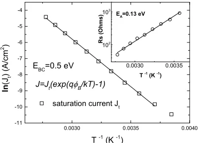
The solar cells were characterised by using capacitance-voltage (C–V) and ac admittance measurements carried out on a Solartron 1260 Impedance Analyzer equipped with a 1296 Dielectric Interface. The trap energy distributions Nt(E) were deduced from the
capacitance-frequency responses applying the analytical model for p−i− n junction as proposed in work [12]. A Gaussian type of defect distribution was considered. To ensure that the carrier freeze-out effects do not contribute to the studied ac admittance responses, the activation energy EAof the
series resistance Rs was determined from the temperature dependent IV-curves by means of the
[image:3.612.126.329.421.566.2]differential method [13] as exemplified in Fig.1. The spatial distribution of the ionized acceptors in the depletion region of CdTe was extracted from the high-frequency capacitance-voltage (CV) curves.
Table 1. Averaged parameters of the solar cells used in this study.
0.0030 0.0035 0.0040
-11 -10 -9 -8 -7 -6 -5 -4
ln
(Jt
)
(A
/c
m
2 )
saturation current Jt
T -1 (K -1) EBC=0.5 eV
J=Jt(exp(qφB/kT)-1)
0.0030 0.0035 102
103
R
s
(
O
h
m
s
)
T -1
(K -1
)
EA=0.13 eV
Figure 1. Arrhenius dependencies of the saturation current Jt and the series resistance Rs
for ZnO/CdS/CdTe solar cells. EBC stands for the back contact barrier height.
RESULTS
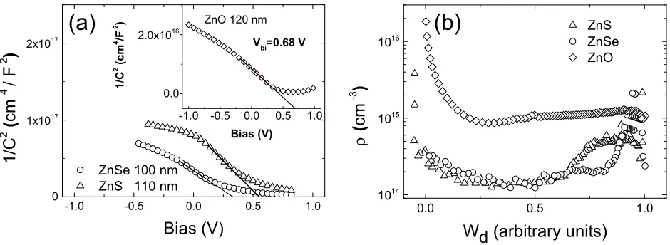
The Mott-Schottky plots for the samples grown on ZnO, ZnSe, and ZnS buffer layers and the distributions of the apparent carrier density in the absorber are shown in Fig. 2 (a, b),
respectively. The cells comprising ZnS or ZnSe revealed lower values of the built-in voltage Vbi
being decreased to 0.54 V and 0.32 V, indicating a smaller barrier height at the heterojunction. The obtained values of ρ throughout the CdTe thickness are very close in both samples, ZnS and
Buffer layer Efficiency (%) Fill Factor (%) JSC (mA/cm2) VOC (V)
120nm ZnO 8.22 ± 1.70 59.25 ± 2.75 20.30 ± 1.67 0.675 ± 0.060
110nm ZnS 0.85 ± 0.29 27.61 ± 3.39 6.03 ± 1.59 0.507 ± 0.024
ZnSe, and they are lower by approx. half of an order of magnitude than that of the cells grown on ZnO. The data presented in Fig. 2 (b) indicate that ZnS or ZnSe buffer layers inhibit the
electrical activation by Cl atoms in CdTe. Similar non-uniform distributions of the net ionized impurity concentration were observed in the depletion region of the junction when the chlorine treatment was implemented in NaCl, KCl and MnCl2 [11]. The lower doping efficiency has been
ascribed to the cation charge state which differs from 2+ in chlorides other than MgCl2 or CdCl2.
Later, inefficiency of anneals in Cl-containing ambient has been explained to originate from the higher dissociation energy of the cation−Cl bond in chlorides [14]. Importantly, the insufficient
activation of acceptors altered the shape of the CV-carrier profiles. The latter is known to be
determined by the spatial distribution of the charge traps in the space charge region (SCR) of a semiconductor, the charge state of the traps, and the emission time constants in respect to the time
domain of ac signal and the sweep voltage. The carrier profiles recorded for the solar cells
concluded on ZnSe and ZnS buffer layers exhibited dips of similar magnitude at about 0.7WD.
Partial recovery of the initial net ionized free carrier concentration is noticed on the profiles at the values of (0.7 − 2.0)×1015 cm−3 towards the full SCR width. As a first approximation, the difference between the profiles can be accounted for the presence of intrinsic point defects which may contribute to the compensation in semi-insulating CdTe. Among the studied deep trap levels in single-crystal CdTe, the recombination active centre is a deep acceptor complex with a trap level at EV + 0.76 eV in undoped and doped CdTe [15]. In polycrystalline CdTe, the
identification of a particular point defect giving rise to the recombination losses in solar cells may be complicated by superimposed contributions from the interface states in the GBs [7].
-1.0 -0.5 0.0 0.5 1.0
0 1x10¹⁷ 2x10¹⁷
ZnSe 100 nm ZnS 110 nm
1
/C
2 (
c
m
4 /
F
2 )
Bias (V)
(a)
-1.0 -0.5 0.0 0.5 1.0 0.0
2.0x10¹⁶
1
/C
2 (
c
m
4 /F 2 )
Bias (V) Vbi=0.68 V ZnO 120 nm
0.0 0.5 1.0
1014
1015 1016
ZnS ZnSe ZnO
ρ
(
c
m
-3 )
Wd (arbitrary units)
[image:4.612.76.546.379.551.2](b)
Figure 2. (a) 1/C2–V plots for samples with different buffer layers. The data were measured at T =300 K and frequency of 10 kHz. The inset, Fig. 2(a), shows the Mott–Schottky plot for the ZnO/CdS/CdTe solar cell. The straight black lines are the fitting curves to estimate the built-in potential Vbi; (b) The apparent doping density profiles ρ(WD) obtained from C–V
characteristics in Fig.2(a).
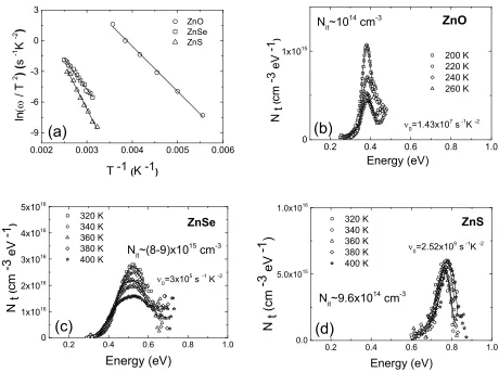
Figure 3(b-d) shows the energy distributions of the charge traps in the CdTe/CdS junction using the EA values extracted from the Arrhenius plots in Fig. 3(a). Only one deep defect level is
(d)), was observed for the CdTe/CdS cells grown on ZnO, ZnSe, and ZnS buffer layers, respectively. The Gaussian fit of the DOS energy distribution provides the values of the broadening parameter δ, which was found to increase from 0.26 meV to 100 meV in the temperature range from 180 K to 400 K for the DOS displayed in Figs. 3(b, c). The broadening of the DOS may be caused by the locally non-uniform distribution of charged defects and defect clusters resulting in potential fluctuations, contributing to Shockley-Read-Hall recombination, and decreasing the open circuit voltage and the fill factor of solar cells.
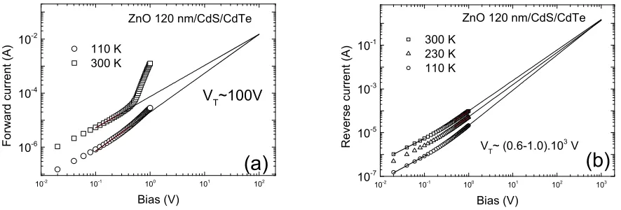
Figure 4 compiles IV characteristics taken on the ZnO/CdTe/CdS cells. The charge carrier transport mechanism at both the forward, Fig 4(a), and the reverse, Fig. 4(b), bias is space-charge-limited conduction (SCLC) as evidenced by the slope of the log(I)-log(V) curves increasing from 1 to 1.4-1.6 that corresponds to a monoenergetic trap level, which can be expected to be shallow in the CdTe/CdS junction since a steep increase in the trap filling charge regime is not observed. The relatively high ohmic current at low voltages is most probably caused by high concentration of impurities in the utilized semiconductors. The trap density Nt
can be estimated by using the expression for the critical voltage VT = qNtd2/2ɛɛ0, were q is the
elemental charge, d is the film thickness, ɛ is the film permittivity, and ɛ0 is the permittivity of
the free space. Given that the relative permittivity for CdTe is 10.16, the trap density Nt can be
0.002 0.003 0.004 0.005 0.006
-9 -6 -3 0 3 ZnO ZnSe ZnS l n (ω / T 2 ) ( s -1 K -2 )
T -1 (K -1)
(a)
0.2 0.4 0.6 0.8 1.0
0 1x10¹⁵
ν0=1.43x10⁷ s -1K -2
N t ( c m
-3 e
V -1) 200 K 220 K 240 K 260 K Energy (eV)
(b)
ZnONit~1014 cm-3
0.2 0.4 0.6 0.8 1.0
0 1x10¹⁶ 2x10¹⁶ 3x10¹⁶ 4x10¹⁶ 5x10¹⁶ ZnSe N t ( c m
-3 e
V -1 ) 320 K 340 K 360 K 380 K 400 K Energy (eV)
(c)
ν0=3x10⁵ s -1 K -2
Nit~(8-9)x1015 cm-3
0.2 0.4 0.6 0.8 1.0
0.0 5.0x10¹⁵ 1.0x10¹⁶
Nit~9.6x1014 cm-3
(d)
ν0=2.52x10⁹ s -1K -2
N
t
(c
m
-3 e
[image:5.612.77.537.309.652.2]V -1 ) 320 K 340 K 360 K 380 K 400 K Energy (eV) ZnS
estimated as ~7·1015 cm-3 and ~4.2·1016 cm-3 for positive and negative polarity of the applied bias, respectively, that is much higher than the density Nit of the traps inferred from the Gaussian
fit of the trap distributions in energy. The asymmetry in IV curves implies different rates of the carrier generation and recombination in the space-charge region of CdTe. Though the
asymmetric IV curves may indicate the presence of Schottky barrier as it has been typically observed in metal-semiconductor-metal structures with dissimilar work functions of electrodes, in the particular case of CdTe solar cells, the blocking action of the TCO/buffer layers/CdS interfaces is unlikely. The charge carrier transport in polycrystalline semiconductors employed in photovoltaics is often supported by tunnelling processes [16]. Having obtained the trap-free space-charge-limited current density on the order of 10−5 A/cm2 from the 300K IV curve in Fig. 4(a) the charge carrier mobility µ of ~0.1 cm2/V·s can be deduced by using the expression J=9/8·θ0·ɛ0·ɛ·µ·V2/d3, where E is the electric field across the device, d is the thickness of the
absorber layer, and θ0is the fraction ofthe free carriers[17]. The obtained mobility values are in
good agreement with those measured by using the time-of-flight method in work [18]. Assuming the charge carrier density in p-type CdTe is lower than that in CdS, the injected charge density is mostly represented by the electron component, and the determined mobility describes the
electron current.
10-2
10-1
100
101
102
10-6
10-4
10-2
(a)
110 K 300 K
F
o
rw
a
rd
c
u
rr
e
n
t
(A
)
Bias (V)
VT~100V
ZnO 120 nm/CdS/CdTe
10-2 10-1 100 101 102 103
10-7
10-5 10-3 10-1
ZnO 120 nm/CdS/CdTe
VT~ (0.6-1.0).103 V
R
e
v
e
rs
e
c
u
rr
e
n
t
(A
) 300 K
230 K 110 K
Bias (V)
[image:6.612.86.529.325.475.2](b)
Figure 4. Forward (a) and reverse (b) current-voltage characteristics of the CdTe/CdS junctions deposited on ZnO. The contact area is 0.24 cm2.
CONCLUSIONS
The deep trap level formation in the solar cells comprising ZnS or ZnSe buffer layers is accompanied by a reduction of the doping density in CdTe implying that the electrical activation of acceptors by chlorine is impeded. This suggests that chlorine can modify kinetics of point defects during anneals of CdTe and redistribute VCd –related defects, similar to laser anneals,
which generate a gradient of the VCd defects in CdTe [19,20]. We suggest that a higher density of
the deep charge traps in CdTe could be ascribed to the VCd defect clustering in polycrystalline
CdTe:Cl, although the VCd clustering in bulk crystals and in the GBs of polycrystalline samples
may differ in kinetics. The defect clustering might occur when the chlorine distribution is locally non-uniform as a result of strain in the GB. Therefore, passivation of the Te-rich GBs may be impeded. Our results clearly indicate that the same defect is responsible for doping and the formation of the charge trapping centers in CdTe. In general, grain boundaries have been
thin film solar cells. Being segregated in grain boundaries, VCd related defects may play a
decisive role in electron tunnelling and charge trapping. Further, it is observed that the majority of electrically active defects in the studied polycrystalline CdTe are the band tail-like defects, which influence conductivity. The charge carrier transport in the studied CdS/CdTe
heterojunctions does not obey the Sah–Noyce–Shockley theory, but can be described within the theory of space-charge limited conduction.
ACKNOWLEDGMENTS
This work was supported by EPSRC PPR10314.
REFERENCES
1. A. Cavallini, B. Fraboni, W. Dusi, N. Auricchio, P. Chirco, M. Zanarini, P. Siffert, P. Fougeres, Nuclear Instruments and Methods in Physics Research A476, 770 (2002).
2. W. L. Rance, J. M. Burst, D. M. Meysing, C. A. Wolden, M. O. Reese, T. A. Gessert, W. K. Metzger, S. Garner, P. Cimo, and T. M. Barnes, Appl. Phys. Lett. 104, 143903 (2014).
3. K. Zweibel, Science328, 699 (2010).
4. I. Visoly-Fisher, S. R. Cohen, K. Gartsman, A. Ruzin, and D. Cahen, Advanced Func. Mater.
16, 649 (2006).
5. L. Zhang, J. L. F. Da Silva, J. Li, Y. Yan, T. A. Gessert, and S.-H. Wei, Phys. Rev. Lett. 101, 155501 (2008).
6. Y. Y. Proskuryakov, K. Durose, B. M. Taele, G. P. Welch, and S. Oelting, J. Appl. Phys. 101, 014505 (2007).
7. M. A. Lourenço, W. Lek Ng, K. P. Homewood, and K. Durose, Appl. Phys. Lett. 75, 277 (1999).
8. N.V. Agrinskaya, O.A. Matveev, Revue de Physique Appliquee12, 235 (1977).
9. W. Regan, S. Byrnes, W. Gannett, O. Ergen, O. Vazquez-Mena, F. Wang, and A. Zettl, Nano
Lett.12(8), 4300 (2012).
10. Y. Roussillon, D. M. Giolando, V. G. Karpov, D. Shvydka, and A. D. Compaan, Appl. Phys. Lett. 85, 3617 (2004).
11. J. D. Major, R. E. Treharne, L. J. Phillips, K. Durose, Nature511, 334 (2014).
12. T. Walter, R. Herberholz, C. Müller, and H. W. Schock, J. Appl. Phys. 80, 4411 (1996). 13. J. H. Werner,Appl. Phys. A47, 291 (1988).
14. B. L. Williams , J. D. Major , L. Bowen , W. Keuning , M. Creatore , and Ken Durose, Adv.
Energy Mater. 1500554 (2015).
15. A. Castaldini, A. Cavallini, B. Fraboni, P. Fernandez, and J. Piqueras, J. Appl. Phys. 83, 2121 (1998).
16. R. E. Treharne, L. J. Phillips, K. Durose, A. Weerakkody, I. Z. Mitrovic, and S. Hall, J. Appl. Phys. 115, 063505 (2014).
17. G. G. Roberts and F. W. Schmidlin, Phys. Rev. 180, 785 (1969).
18. Qi Long, S. A. Dinca, E. A. Schiff, M. Yu, and J. Theil, Appl. Phys. Lett. 105, 042106 (2014). 19. B. J. Simonds, S. Misra, N. Paudel, K. Vandewal, A. Salleo, C. Ferekides, M. A. Scarpulla,
Proc. of SPIE 9180, 91800F (2014).
20. A. Medvid, Y. Hatanaka, D. Korbutjak, L. Fedorenko, S. Krilyuk, V. Snitka, Appl. Surf. Sci.