International Journal of Research (IJR)
e-ISSN: 2348-6848, p- ISSN: 2348-795X Volume 2, Issue 10, October 2015Available at http://internationaljournalofresearch.org
Available online:http://internationaljournalofresearch.org/ P a g e | 149
A Multifunctional D-Statcom Operating
Under Stiff Source for Voltage Regulation at Load Terminals
1
Mr.
Cherlopalli Naveen Kumar &
2Mr. M.Kiran
1
M.TECH scholar, Dept.Of EEE, SVPCET, Puttur, India
2
Assistant Professor, Dept.Of EEE, SVPCE, Puttur, India
Abstract:
Loads connected to a stiff source cannot be protected from voltage disturbances using a distribution static compensator (DSTATCOM). In this paper, a new control-algorithm-based multifunctional DSTATCOM is proposed to operate in voltage control mode under stiff source. This scheme provides fast voltage regulation at the load terminal during voltage disturbances and protects critical loads. In addition, during normal operation, the generated reference load voltages allow control of the source currents. Consequently, DSTATCOM injects reactive and harmonic components of load currents to make source power factor unity. Simulation and experimental results are presented to verify the efficacy of the proposed control algorithm and multifunctional DSTATCOM.
Index Terms—Distribution static compensator
(DSTATCOM); multifunctional; power factor; stiff source; voltage regulation
I. INTRODUCTION
Large electric drives and utility applications require advanced power electronics converter to meet the high power demands. The evolution of power electronic devices, nonlinear loads, and unbalanced loads has degraded the power quality in the power distribution network [1]. The distribution static compensator is a shunt active filter, which injects currents into the point of common coupling (PCC) (the common point where load, source, and DSTATCOM are connected) such that the harmonic filtering, power factor correction, and load balancing can be achieved. In practice, the presence of feeder impedance and nonlinear loads distorts the terminal voltage (PCC) and source currents. The load compensation using state feedback control of DSTATCOM with shunt filter capacitor gives better results [2]. The switching frequency components in the terminal voltages and source currents are eliminated by using state feedback
control of shunt filter capacitor. in this situation, DSTATCOM should operate in CCM. However, due to grid faults, source voltage (stiff or non-stiff) can change at any time and then VCM operation is required. DSTATCOM regulates the load voltage by indirectly regulating the voltage across the feeder impedance. When a load is connected to nearly a stiff source, feeder impedance will be negligible [1]–[4]. Under these circumstances, DSTATCOM cannot provide sufficient voltage regulation at the load terminal [9]. This paper proposes a new control algorithm based DSTATCOM topology for voltage regulation even under stiff source. It is achieved by connecting a suitable external inductor in series between the load and the source point. Point of common coupling (PCC) will be the point where external inductor and source are connected. DSTATCOM, connected at the load terminal, provides voltage regulation by indirectly regulating the voltage across the external inductor. Proposed control algorithm to obtain variable reference load voltage is formulated as a function of the desired source current. This voltage indirectly controls the current drawn from the source for a permissible range of source voltage. There fore, the control algorithm makes source currents balanced, sinusoidal, and in phase with respective source voltages during normal operation. During voltage disturbances, a constant voltage is maintained at the load terminal. Hence, proposed topology and control algorithm make compensator multifunctional so that it provides fast voltage regulation at load terminal and additionally provides advantages of CCM while operating in VCM.
II. DSTATCOM CONFIGURATION
International Journal of Research (IJR)
e-ISSN: 2348-6848, p- ISSN: 2348-795X Volume 2, Issue 10, October 2015Available at http://internationaljournalofresearch.org
Available online:http://internationaljournalofresearch.org/ P a g e | 150
distribution network is shown in Fig. 1.VSI represented by u V dc is connected to load terminal through an LC filter ().
Fig.1.Single phase equivalent circuit of DSTATCOM in distribution network.
The load terminal is connected to the PCC through an external series inductance Lext. Vdc is the voltage
maintained across the each dc capacitor and u is a control variable which can be +1 or -1 depending upon switching state. If i, if t, and if c are currents through VSI, DSTATCOM, and Cfc respectively. Vs and Vt are source and load voltages respectively. Loads have both linear and nonlinear elements with balanced or unbalanced features. Load and source currents are represented by I and is respectively.
III. SELECTION OF EXTERNAL INDUCTOR
Under normal operation, external impedance (Zext) does not have much importance, whereas it plays a critical role during voltage disturbances. The value of external impedance is decided by the rating of the DSTATCOM and amount of sag to be mitigated. At any time, the source current in any phase by assuming balanced source voltage is given as
𝐼 𝑆=
𝑉𝑆< 0 − 𝑉𝑡 < −𝛿 𝑅𝑒𝑥𝑡 + 𝑗𝑋𝑒𝑥𝑡
(1)
where Vs, Vt, Rext, Xext, and δ are the RMS source voltage, RMS load voltage, external resistance, external reactance, and load angle, respectively. For most practical case, Xext _ Rext. As a worst case design, the reactive source current (Im[Is]), which is supplied by the compensator, will be maximum when δ is minimum. For this, the source will supply only losses inthe VSI. Therefore, δ will be very small. Hence, Im [Is] is given as
𝐼𝑚 𝐼 𝑆 =𝑉𝑇 − 𝑉𝑆
𝑋𝑒𝑥𝑡 (2)
During voltage disturbances, the aim is to protect the sensitive loads with focus is on to improve the DSTATCOM capability to mitigate deep sag. Therefore, keeping it into account, the load voltage during voltage sag is taken as 0.9 pu (per unit) which is sufficient to protect the load. Assuming that the reactive current that a compensator can inject is 20 A and load needs to be protected from sag of 40%, then the value of external reactance is found to be
𝑋𝑒𝑥𝑡 =
0.9 − 0.6
20 × 230 = 3.45Ω (4)
External reactance of 3.45 that corresponds to an inductance of 11 mH for a 50 Hz supply is used.
IV. P ROPOSED CONTROL ALGORITHM
Proposed control algorithm aims to provide fast voltage regulation at the load terminal during voltage disturbances while retaining the advantages of CCM during normal operation. Firstly, currents that must be drawn from the source to get advantages of CCM are computed. Using these currents, magnitude of voltages that need to be maintained at load terminal is computed. If this voltage magnitude lies within a permissible range then same voltage is used as reference voltage to provide advantages of CCM. If voltage lies outside the permissible range, it is a sign of voltage disturbance and a fixed voltage magnitude is selected as reference voltage. A two loop controller, whose output is load angle, is used to extract load power and VSI losses from the source. Finally, a discrete model is derived to obtain switching pulses. All these steps are presented in detail in this section. A. Computation of Reference Voltage Magnitude (Vt*) During normal operation, load voltage must be regulated in such a way that following advantages provided by CCM operation are achieved:
Source currents are balanced and sinusoidal.
Unity power factor (UPF) at PCC. Source supply load average power and
VSI losses.
International Journal of Research (IJR)
e-ISSN: 2348-6848, p- ISSN: 2348-795X Volume 2, Issue 10, October 2015Available at http://internationaljournalofresearch.org
Available online:http://internationaljournalofresearch.org/ P a g e | 151
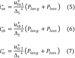
sequence component of load voltages (v+ta1, v+tb1, and v+tc1) are extracted and used to compute reference source currents (i*sa, i*sb, and i*sc) as follows:
𝑖𝑠𝑎∗ = 𝑢𝑡𝑎 1+
Δ1+
𝑃𝑙𝑎𝑣 𝑔+ 𝑃𝑙𝑜𝑠𝑠 (5)
𝑖𝑠𝑏∗ = 𝑢𝑡𝑏 1+
Δ1+
𝑃𝑙𝑎𝑣𝑔 + 𝑃𝑙𝑜𝑠𝑠 (6)
𝑖𝑠𝑐∗ = 𝑢𝑡𝑐 1+ Δ1
+ 𝑃𝑙𝑎𝑣𝑔 + 𝑃𝑙𝑜𝑠𝑠 (7)
where Δ+1 =_j=a,b,c(v+tj1)2, and Plavg is the average load power that is calculated using a moving average filter (MAF). The total losses in the inverter, i.e., Ploss, computed using a PI controller, helps in maintaining the averaged dc-link voltage (Vdc1 + Vdc2) at a predefined reference value (2Vdcref ) by drawing a set of balanced currents from the source and is given as follows:
𝑃𝑙𝑜𝑠𝑠 = 𝐾𝑝𝑑𝑐𝑒 + 𝐾𝑖𝑑𝑐 𝑒 𝑑𝑡 (8)
Where Kpdc, Kidc, and e = 2Vdcref − (Vdc1 + Vdc2)
are the proportional gain, integral gain, and voltage error of the PI controller, respectively. Once the reference currents to be drawn from the source are computed using (4), reference voltages at the load terminal can be derived. Applying Kirchhoff’s voltage law in the circuit shown in Fig. 1:
Fig. 2. Controller to calculate δ and Ploss. From the previous equation, the load voltage can be computed as follows:
𝑉𝑡 = (𝑉𝑠− 𝐼𝑠𝑅𝑒𝑥𝑡)2+ (𝐼𝑠𝑅𝑒𝑥𝑡)2 (9)
Based on standards, load voltage has a permissible range of variations between 0.9 and 1.1 p.u. [14]. Therefore, as long as Vt, obtained using (7), lies between 0.9 and 1.1 p.u., it is used as reference load voltage (V ∗ t ), and the advantages of CCM operation are achieved. Here, Vt is indirectly
controlled by the desired source current. During sag and swell, the load voltage magnitude will be between 0.9 and 0.1 p.u. and 1.1 and 1.8 p.u., respectively, for half cycle to 1 min [16]. Therefore, reference load voltage magnitude is set to 0.9 and 1.1 p.u. during sag and swell, respectively. The reason to keep load voltages at these values is to maximize the DSTATCOM disturbance withstanding ability while keeping load voltage at the safe limits for satisfactory operation. B. Computation of Load Angle (δ)
The block diagram of a controller to compute load angle δ is shown in Fig. 2. It ensures that the load average power and losses in the VSI are supplied by the source [7]. Alternately, Ploss responsible for maintaining dc-link voltage must be
equal to shunt-link power Psh. Comparing Ploss and Psh, an
error is generated, which is passed through a PI controller to compute δ as follows
𝛿 = 𝐾𝑝𝑎| 𝑃𝑙𝑜𝑠𝑠 − 𝑃𝑠 + 𝐾𝑖𝑎 𝑃𝑙𝑜𝑠𝑠 − 𝑃𝑠 𝑑𝑡 (10)
where Kpa and Kia are the proportional and integral gains of
the inner PI controller, respectively. The value of shunt-link power Psh is computed using a MAF as follows:
𝑃𝑠 =
1
𝑇 (𝑈𝑡𝑎𝑖𝑓𝑡𝑎 +
𝑡1+𝑇
𝑡1
𝑈𝑡𝑏𝑖𝑓𝑡𝑏 + 𝑈𝑡𝑐𝑖𝑓𝑡𝑐 (11)
A positive value of Psh represents power flow from DSTATCOM to load terminal, whereas a negative value of Psh represents power flow from load terminal to DSTATCOM. In steady state, VSI losses are compensated by taking power from the source. Hence, Psh will be negative in steady state. Moreover, capacitor voltage decreases from its reference value in steady state. The deviation of capacitor voltage from reference voltage represents losses in the VSI. Hence, Ploss will be negative during steady state. Therefore, at all times, Psh and Ploss should be equal. Hence, the difference of Psh and Ploss should be minimized. The output of the inner PI controller, as shown in Fig. 2, is delta, which ensures that shunt-link power Psh drawn from the source equals to losses in the capacitor Ploss.
C. Generation of Instantaneous Reference Voltage
By knowing the zero crossing of phase-a source voltage, selecting a suitable reference load voltage magnitude from (8),
and computing load angle δ from (9), the three-phase reference voltages are given as follows:
International Journal of Research (IJR)
e-ISSN: 2348-6848, p- ISSN: 2348-795X Volume 2, Issue 10, October 2015Available at http://internationaljournalofresearch.org
Available online:http://internationaljournalofresearch.org/ P a g e | 152
𝑈𝑡𝑟𝑒𝑓𝑏 = 2𝑉∗𝑡sin 𝜔𝑡 −
2𝜋
3 − 𝛿 (13)
𝑈𝑡𝑟𝑒𝑓𝑐 = 2𝑉∗𝑡sin 𝜔𝑡 −
2𝜋
3 − 𝛿 (14)
where ω is the system frequency
D. Generation of Switching Pulses
Each phase of the VSI can be controlled independently, and hence, a discrete model of single phase has been derived to generate switching pulses. The dynamics of filter inductor and capacitor can be presented by the following equations:
𝑑𝑢𝑓𝑐
𝑑𝑡 = 1 𝐶𝑓𝑐
𝑖𝑓𝑖 −
1 𝐶𝑓𝑐
𝑖𝑓𝑖 (15)
V. SIMULATION RESULTS
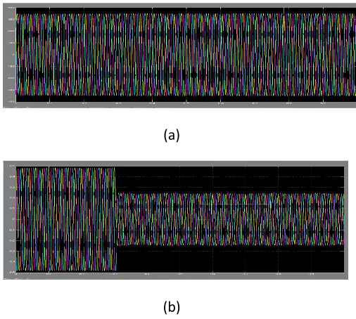
The proposed control algorithm and multifunctional DSTATCOM make three-phase source currents balanced, sinusoidal, and in phase with respective source voltages at the PCC, within the permissible range of voltage. In addition, a fast voltage regulation at the load terminal is provided to protect sensitive loads during voltage disturbances. In addition, load harmonic and reactive current components are supplied by the compensator all the time. All aforementioned advantages are verified in digital environment using PSCAD software. A three-phase stiff source of 230 V rms per phase (1.0 p.u.) is considered. Filter parameters are Lf = 20 mH, Cf = 10 μF, Vdc = 600 V, and Cdc = 3000 μF. External inductance
Lext = 11 mH is used. Initially, a three-phase unbalanced linear and nonlinear load of 6.9 kW is connected. At t = 0.2 s.It can be seen that both voltage and current are in phase with
each other. The load is brought back to its normal value at t = 0.32 s. The controller takes one cycle to detect this change and brings back the source current at its normal value. The current is in phase with source voltage. The entire transient is shown in Fig. 3(b). To show the voltage regulation capability of DSTATCOM, at t = 0.8 s, a sag is created by lowering the source voltage by 30%, as shown in Fig. 4(a). A fast voltage regulation is provided at the load terminal to protect sensitive loads, while maintaining a voltage of 0.9 p.u., and is shown in
Fig. 4(b). During sag period, source current will increase, as shown in Fig. 4(a). Voltage sag is cleared at t = 0.9 s, and then, load voltage starts following the source voltage, as illustrated in Fig. 4(a). Consequently, the source current and the source voltage slowly come in phase with each other. Fig. 5(a) shows the load angle δ, which is regulated by a controller to ensure that the average load power and inverter losses are taken from the source during normal operation, load change, and voltage disturbances. Fig. 5(b) shows the
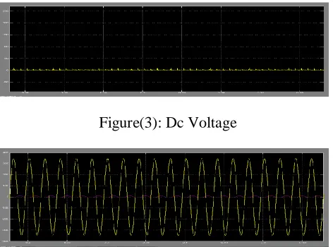
voltage at dc bus, which is regulated around 1200 V during the entire operation.
(a)
(b)
Figure (1): Phase-waveforms with sag Condition (a) Source voltage and source current (current is scaled up ten times for
clear visibility). (b) Load voltage.
(a)
(b)
Figure (2): Phase-waveforms with out sag Condition (a) Source voltage and source current (current is scaled up ten
International Journal of Research (IJR)
e-ISSN: 2348-6848, p- ISSN: 2348-795X Volume 2, Issue 10, October 2015Available at http://internationaljournalofresearch.org
Available online:http://internationaljournalofresearch.org/ P a g e | 153
Figure(3): Dc Voltage
Fig. 5. Phase-a waveforms before, during, and after load change. (a) Load current. (b) Source voltage and source current (current is scaled up ten times for clear visibility).
VI. CONCLUSION
In this paper, a new control algorithm based multifunctional DSTATCOM has been proposed to protect the load from voltage disturbances under stiff source. It has been achieved by placing an external series inductance of suitable value between the source and the load. In addition, instantaneous reference voltage is controlled in such a way that the source currents are indirectly controlled, and the advantages of CCM operation are achieved while operating in VCM for a permissible range of source voltage. The proposed algorithm and multifunctional DSTATCOM are able to mitigate voltage- and current-related PQ issues, and confirmatory results have been presented.
REFERENCES
[1] A. Bhattacharya and C. Chakraborty, “A shunt active power filter with enhanced performance using ANN-based predictive and adaptive controllers,” IEEE Trans. Ind. Electron., vol. 58, no. 2, pp. 421–428, Feb. 2011.
[2] S. Rahmani, A. Hamadi, and K. Al-Haddad, “A Lyapunov-function-based control for a three-phase shunt hybrid active filter,” IEEE Trans. Ind. Electron., vol. 59, no. 3, pp. 1418–1429, Mar. 2012.
[3] M. K. Mishra and K. Karthikeyan, “An investigation on design and switching dynamics of a voltage source inverter to compensate unbalanced and nonlinear loads,” IEEE Trans. Ind. Electron., vol. 56, no. 8, pp. 2802– 2810, Aug. 2009.
[4] J. Liu, P. Zanchetta, M. Degano, and E. Lavopa, “Control design and implementation for high performance shunt active filters in aircraft power grids,” IEEE Trans. Ind. Electron., vol. 59, no. 9, pp. 3604–3613, Sep. 2012.
[5] A. Bhattacharya, C. Chakraborty, and S. Bhattacharya, “Parallelconnected shunt hybrid active power filters operating at different switching frequencies for improved performance,” IEEE Trans. Ind. Electron., vol. 59, no. 11, pp. 4007–4019, Nov. 2012.
[6] Q.-N. Trinh and H.-H. Lee, “An advanced current control strategy for three-phase shunt active power filters,” IEEE Trans. Ind. Electron., vol. 60, no. 12, pp. 5400–5410, Dec. 2013.
[7] M. K. Mishra, A. Ghosh, and A. Joshi, “Operation of a DSTATCOM in voltage control mode,” IEEE Trans. Power Del., vol. 18, no. 1, pp. 258– 264, Jan. 2003.
[8] H. Fujita and H. Akagi, “Voltage-regulation performance of a shunt active filter intended for installation on a power distribution system,” IEEE Trans. Power Electron., vol. 22, no. 3, pp. 1046–1053, May 2007.
[9] R. Gupta, A. Ghosh, and A. Joshi, “Performance comparison of VSCbased shunt and series compensators used for load voltage control in distribution systems,” IEEE Trans. Power Del., vol. 26, no. 1, pp. 268– 278, Jan. 2011.