International Journal of Emerging Technology and Advanced Engineering
Website: www.ijetae.com (ISSN 2250-2459, Volume 2, Issue 6, June 2012)404
Reduction of Power Dissipation in 32bit RISC
Microprocessor using Clock Gating
Puran Gaur
1, Swati Joshi
2 1, 2 NRI BhopalAbstract— In the world of computation and processors the power dissipation is main problem that will reduce the performance of the processor. In the processor continuous switching in the logical circuits cause heat dissipation in processor that will fetch more power from the supply side and this problem will cause reduction of the optimized performance of the microprocessor.In this research paper we are trying to present a new kind of logical algorithm by which we can reduce the power dissipation by reducing the switching of transistors present or use in various logical circuits.
Keywords—Clock Gating, VHDL, ASIC, CSIC,VLSI,ALU.
I. INTRODUCTION
A microprocessor is a multipurpose, programmable, clock driven, register based electronic device that reads binary instruction from a storage device called memory, accepts binary data as input and processes data according to those instructions, and provides results as output. The microprocessor operates in binary digits, 0 and 1, also known as bits. Each microprocessor recognizes and processes a group of bits called the word, and microprocessor are classified according to their word length [1]. For example, a processor with an 8 bit word is known as an 8 bit microprocessor and a processor with a 32 bit word is known as a 32 bit microprocessor. RISC 32 bit Processor use on Application or Customer Specific Integrated Circuited (ASIC or CSIC)[5].This design is a 32-bit processor, i.e., the data and instruction word sizes are 32 bits. It is pipelined to a depth of 5 stages. The instruction set implements ALU, immediate, load- store, and branch instructions. The processor is divided into 6 units: the
instruction fetch unit (ifetch.vhd), the decoder
(decode.vhd), the branch condition detector (branch.vhd), the ALU (alu.vhd), the register _le (reg_le.vhd), and the data load-store unit (dls.vhd). The units are connected together with appropriate glue logic insystem.vhd. For easier conversion of the design to a DSP (digital signal processor), the processor implements the Harvard architecture of separate instruction and data memory spaces.
For this prototype, main memory is simulated by a server program running on a PC that serves requests for transactions to the data and instruction memory spaces. For practical reasons, namely the availability of only one external bus to the PC, the bus transfers from the processor is serialized by an arbiter to transfer over one bus. However, logically from the point of view of both the processor and the simulated memory device, there are two separate memory spaces.
II. SYSTEM MODEL AND IMPLEMENTED DESIGN 1. Instruction Fetch Unit: The first stage in the pipeline is the Instruction Fetch. Instructions are fetched from the memory and the Instruction Pointer (IP) is updated. The function of the instruction fetch unit is to obtain an instruction from the instruction memory using the current value of the PC and increment the PC value for the next instruction as shown in Figure. This stage is where a program counter will pull the next instruction from the correct location in program memory. In addition the program counter will updated with either the next instruction location sequentially, or the instruction location as determined by a branch. The instruction fetch stage is also responsible for reading the instruction memory and sending the current instruction to the next stage in the pipeline, or a stall if a branch has been detected in order to avoid incorrect execution. The instruction fetch unit contains the following logic elements that are implemented in VHDL: 8-bit program counter (PC) register, an adder to increment the PC by four, the instruction memory, a multiplexor, and an AND gate used to select the value of the next PC. Program counter and instruction memory are the two important blocks of Instructions Fetch Unit [2]
International Journal of Emerging Technology and Advanced Engineering
Website: www.ijetae.com (ISSN 2250-2459, Volume 2, Issue 6, June 2012)405 3. Instruction memory (IM): The Instruction memory on these machines had a latency of one cycle. During the Instruction Fetch stage, a 32-bit instruction is fetched from the memory. The PC predictor sends the Program Counter (PC) to the Instruction memory to read the current Instruction. At the same time, the PC predictor predicts the address of the next instruction by incrementing the PC by one.
4. Instruction registers (IR): An instruction register (IR) is the part of control unit that stores the instruction currently being executed or decoded. In simple processors each instruction to be executed is loaded into the instruction register which holds it while it is decoded, prepared and ultimately executed, which can take several steps. RISC processors use a pipeline of instruction registers where each stage of the pipeline does part Of the decoding, preparation or execution and then passes it to the next stage for its step. Modern processors can even do some of the steps of out of order as decoding on several instructions is done in parallel. Decoding the opcode in the instruction register includes determining the instruction, where its operands are in memory, retrieving the operands from memory, allocating processor resources to execute the command. The output of IR is available to control circuits which generate the timing signals that controls the various processing elements involved in executing the instruction.
5. Instruction Decode Unit: The Instruction Decode stage is the second stage in the pipeline. Branch targets will be calculated here and the Register File, the dual-port memory containing the register values, resides in this stage. The forwarding units, solving the data hazards in The pipeline, reside here. Their function is to detect if the register to be fetched in this stage is written to in a later stage. In that case the data is forward to This stage and the data hazard is solved. This stage is where the control unit determines what values the control lines must be set to depending on the instruction. In addition, hazard detection is implemented in this stage, and all necessary values are fetched from the register banks. The Decode Stage is the stage of the CPU's pipeline where the fetched instruction is decoded, and values are fetched from the register bank. It is responsible for mapping the different sections of the instruction into their proper representations (based on R or I type instructions).
The Decode stage consists of the Control unit, the Hazard Detection Unit, the Sign Extender, and the Register bank, and is responsible for connecting all of these components together. It splits the instruction into its various parts and feeds them to the corresponding components. Registers Rs and RT are fed to the register bank, the immediate section is fed to the sign extender, and the ALU opcode and function codes are sent to the control unit. The outputs of these corresponding components are then clocked and stored for the next stage The Control unit takes the given Opcode, as well as the function code from the instruction, and translates it to the individual instruction control lines needed by the three remaining stages. This is accomplished via a large case statement[3].
6. Control unit: The control unit of the MIPS single-cycle processor examines the instruction opcode bits and decodes the instruction to generate nine control signals to be used in the additional modules. The Reg Dst control signal determines which register is written to the register file. The Jump control signal selects the jump address to be sent to the PC. The Branch control signal is used to select the branch address to be sent to the PC. The MemRead control signal is asserted during a load instruction when the data memory is read to load a register with its memory contents. The MemReg control signal determines if the ALU result or the data memory output is written to the register file. The ALUOp control signals determine the function the ALU performs. (E.g. and, or, add, sbu, slt) The MemWrite control signal is asserted when during a store instruction when a registers value is stored in the data memory.The ALUSrc control signal determines if the ALU second operand comes from the register file or the sign extend. The RegWrite control signal is asserted when the register file needs to be written[4].
International Journal of Emerging Technology and Advanced Engineering
Website: www.ijetae.com (ISSN 2250-2459, Volume 2, Issue 6, June 2012)406 If the instruction decoded was a branch or jump, the target address of the branch or jump was computed in parallel with reading the register file. The branch condition is computed after the register file is read, and if the branch is taken or if the instruction is a jump; the PC predictor in the first stage is assigned the branch target, rather than the incremented PC that has been computed.
8. Execution Unit: The third stage in the pipeline is where the arithmetic- and logic-instructions will be executed. All instructions are executed with 32-bit operands and the result is a 32-bit word. An overflow event handler was not included in this project. The execution unit of the MIPS processor contains the arithmetic logic unit (ALU) which performs the operation determined by the ALUop signal. The branch address is calculated by adding the PC+4 to the sign extended immediate field shifted left 2 bits by a separate adder. The logic elements to be implemented in VHDL include a
9. ALU unit: The arithmetic/logic unit (ALU) executes all arithmetic and logical operations. The arithmetic/logic unit can perform four kinds of arithmetic operations, or
mathematical calculations: addition, subtraction,
multiplication, and division. As its name implies, the arithmetic/logic unit also performs logical operations. A logical operation is usually a comparison. The unit can compare numbers, letters, or special characters. The computer can then take action based on the result of the comparison. This is a very important capability
10. Memory Access unit: The memory access stage is the fourth stage of pipeline. This is where load and store instructions Will access data memory. During this stage, single cycle latency instructions simply have their results forwarded to the next stage. This forwarding ensures that both single and two cycle instructions always write their results in the same stage of the pipeline, so that just one write port to the register file can be used, and it is always Available. If the instruction is a load, the data is read from the data memory
11. Data Memory Unit (DM): The data memory unit is only accessed by the load and store instructions. The load instruction asserts the MemRead signal and uses the ALU Result value as an address to index the data memory. The read output data is then subsequently written into the register file. A store instruction asserts the MemWrite signal and writes the data value previously read from a register into the computed memory address. The VHDL implementation of the data memory was described earlier.
12. Write back unit: During this stage, both single cycle and two cycle instructions write their results into the register file.
13.Inverter and bit control unit: This is the unit that will change some defined bit when required in the processor during the applied operations in the circuit. The complete operation is handled by this intelligent unit for reduction in power dissipation that will occurs because of bit changing during each clock as defined in the VHDL logic.
III. REALIZATION
International Journal of Emerging Technology and Advanced Engineering
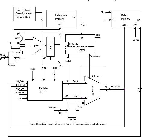
Website: www.ijetae.com (ISSN 2250-2459, Volume 2, Issue 6, June 2012) [image:4.612.71.307.111.340.2]407
Fig 1 Shows the Inverter Circuit along with 32 bit RISC processor[6]
The changes can be understand by the given table that shows how we can reduce the bit switching by using a not gate bypass circuit. The table shows an example that if the there is a bit combination will try to operate any condition than every time the bit change should be there than only the output will works so if this bit change can be bypassed to a inverter circuit than the bit conversion should not be happing itself this operation is handled by the inverter bypassed circuit.
Here we applied the inverter bypassed to the bit 1 and bit 2 only because if we applied it for all 4 bits the time slot is increases. This only an assumed example as shown in table
Table 1 Actual Operation in the Circuit S.
No CLK (Clock) Bit 1 Bit 2 Bit 3 Bit 4 Output
1 1 0 0 0 0 Read high
2 1 0 0 0 1 Write
high
3 1 0 0 1 0 PC high
4 1 0 0 1 1 IR high
5 1 0 1 0 0 Data mem
enable
6 1 0 1 0 1 Bus S high
7 1 0 1 1 0 Bus T
high
8 1 0 1 1 1 Encoder
high
9 1 1 0 0 0 ALU
output high
The table 1 shows that combination of various bit will control the operation in processor now here we see that the Bit 2 change is there after serial number 4 operation and this can will demand switching of bits and as well as transistor according to clock gating so here we apply an control towards the inverter assembly so the bit change will not occur directly on the RISC processor this change will happen in inverter assembly as shown in table 2
Here in table 2 we see that when the bit is changing in serial no 5 operation the bit 2 control is directly transfer to the inverter control assembly which will change the bit from 0 to 1 externally so the that the heat dissipation and transistor switching is not between taken place directly to word the RISC assembly this will reduce the power heat dissipation on each of the clock and this operation can also been control using the gray code conversion so that the power loss can be reduce and this will provide and optimized performance for the processor
Table 2 Actual Operation with inverter assembly
IV. CONCLUSION
[image:4.612.325.556.333.576.2]International Journal of Emerging Technology and Advanced Engineering
Website: www.ijetae.com (ISSN 2250-2459, Volume 2, Issue 6, June 2012)408
REFERENCES
[1] Gaonker, Ramesh, Microprocessor Architecture, programming and Application, Penram International Publishing.
[2] Implementation of a 32-bit RISC Processor for the Data-Intensive Architecture Processing-In-Memory ChipJerey Draper,Je Sondeen, Sumit Mediratta, Ihn KimUniversity of Southern California Information Sciences Institute.
[3] VLSI Processor Architecture JOHN L. HENNESSY
[4] 64-bit Floating Point Processing Unit for a RISC Microprocessor Fujitsu Laboratories Ltd.
[5] RISC AND CISC Computer Architecture By Farhat Masood [6] Design and Implementation of a 64-bit RISC Processor using VHDL