1599 | P a g e
LOADED RESONANT CONVERTOR FOR DC TO DC
ENERGY CONVERSION
Vijaya Kumar Vadladi
1, Machunoori Mounica
21,2
Assistant Professor, GRIET Hyderabad (India)
ABSTRACT
This paper presents a new topology for a high efficiency dc/dc resonant power converter that utilizes a
resistance compression network to provide simultaneous zero voltage switching and near zero current switching
across a wide range of input voltage, output voltage and power levels. The resistance compression network
(RCN) maintains desired current waveforms over a wide range of voltage operating conditions. The use of
PWM control in conjunction with narrowband frequency control enables high efficiency to be maintained
across a wide range of power levels. The converter Implementation provides galvanic isolation and enables
large (greater than 1:10) voltage conversion ratios, making the system suitable for large step-up conversion in
applications such as distributed photovoltaic converters. Simulation results from a 100 W prototype operating
at 500 kHz show that over 95% efficiency is maintained across an input voltage range of25 V to 40 V with an
output voltage of 300 V. The output of 300V dc is fed to the separately excited dc motor and speed, torque,
armature voltage and armature current is calculated. So we have tested the developed converter for static load
and a dynamic load.
Index Terms: DC/DCconverter, resonant converter, on-off control, high efficiency power
converter, resistance compression network
I.INTRODUCTION
The power electronics community s constantly striving towards developing higher efficiency converters. High efficiency is achieved by utilizing switching topologies with ideally lossless passive components. In order to have high efficiency a trade-off between conduction and switching loss has to be made in order to minimize the total loss. The ideal dc-dc converter exhi bits 100% efficiency; in practice, efficiencies of 70% to 95% are typically obtained. This is achieved using switched-mode,or chopper,circuits whose elements dissipate negligible power.Resonant converter,can achieve very lowswitching loss thus enable resonant topologies to operate at high switching frequency.In resonant topologies, Series Resonant Converter.problem. As frequency
increases in SRC, the impedance of the resonant tank is increased. This means more and more energy is
circulating in the resonant tank instead of transferred to output. So SRC is expected to handle wide input range
but with impedance problem. So as to deal with impedance, new topology is introduced in this paper.
Impedance problem can be resolved using the new concept, resistance compression effect. It matches input and
output impedance with a varying load condition. boost converter with the inductor split to form a transformer,
so that the voltage ratios are multiplied with an additional advantage of isolation. It also make use of single
1600 | P a g e
II.
TOPOLOGY AND CONTROL OF RCN CONVERTER
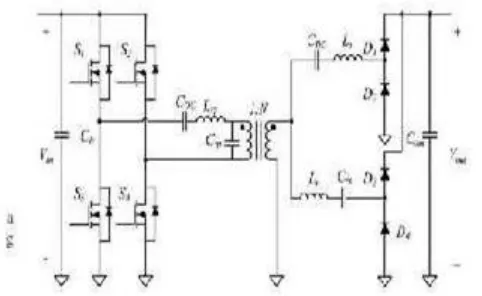
The dc/dc converter proposed here consists of an inversionstage, a transformation stage and a rectification stage,
as shown in Figure 1. The inversion and rectification stages use standard designs. However, the transformation
stage and the control of the converter are new. The topology of the proposed Resistance Compression Network
(RCN) converter. The converter as shown is designed to step-up voltage. The transformation stage consists of a
matching network, a transformer, and a resistance compression network (RCN). The matching network
composed of Lrp and Crp acts as a filter and provides a voltage gain, hence reducing the transformer turns ratio
requirement. One issue with high-turns-ratio step-up transformers that exists in many topologies is that the
parasitic leakage inductance of the transformer can undesirably ring with its secondary side winding capacitance
at the switching transitions. This creates large ringing in the current and voltage waveforms, and high-frequency
losses. The matching network also eliminates this ringing by absorbing the transformer parasitics. The 1:N
transformer provides additional voltage gain and isolation. The resistance compression network (composed of
Ls and Cs) is a Special single input, multi- output matching network that provides desirable impedance control
characteristics [15].
Fig. 1. Proposed DC/DC Converter.
The RCN technique was originally proposed and applied for radio-frequency (RF) applications, such as
very-high- frequency dc/dc converter systems [15] and RF power amplifiers [16]; here we exploit if for high
efficiency power conversion. The function of the RCN is to automatically regulate the converter operating
power and waveforms in a desirable manner as the input and output voltages vary. As applied here, the RCN
also includes a series resonant tank (composed of Lr and Cr) [8]. Its purpose is to provide additional filtering.
The inverter stage is simply a full- bridge inverter (composed of switches S1 - S4). A full- bridge is used instead
of a half-bridge to reduce the voltage gain requirement from the matching network and the transformer. The
rectification stage is composed of two half bridge rectifiers. The capacitors Cin and Cout are for input and
output filtering, respectively, and the two capacitors marked as CDC are for dc blocking purposes.
1601 | P a g e which consists of a MOSFET switch and a fly back transformer. The transformation stage include a resistance
compression network
The output power in the proposed converter is regulated using on-off control, also known as burst-mode control
or bang-bang control. Power is controlled by gating the converter on and off at a modulation frequency that is
much lower than the switching frequency [13], [15], The advantage of using on-off control is that the magnetics
are designed for only a single frequency (a high frequency) while the power is regulated by turning the
converter on and off at a lower frequency.
Moreover, the power is transferred only in the fraction of the time the converter is on, which results in high
efficiency even at light loads. The output power is controlled by the duty ratio of the on-off modulation. On/off
control can be implemented through hysteretic control through fixed- period on off PWM or other methods.
Additional care may be necessary in implementations that allow very short onor off durations to maintain high
efficiency and desired operation during on-off transient conditions. The on-off modulation has its own
corresponding loss. The higher the modulation frequency the greater the loss. The output capacitance is sized
according to the on-off modulation frequency; with a lower modulation frequency a larger capacitor has to be
used. The duty ratio of the modulation also influences the loss. Very small or very large duty ratio results in
greater loss as the converter operates in steady state for a shorter time. So, in order to minimize the total loss
both the modulation frequency and the duty ratio have to be considered.
III. DESIGN METHODOLOGY AND ANALYSIS
Using fundamental frequency analysis, at the switchingfrequency the half-bridge rectifiers can be modeled as resistors,. The effective resistance of these rectifiers is given by
Where Vout is the converter output voltage and Pout is the switching-cycle-average output power. As shown in Fig. 2, one of the branches of the RCN comprises a blocking capacitor CDC and an RCN inductor Ls. The other branch comprises a series LC tank tuned to be net capacitive at the switching frequency (net equivalent capacitance Cs). This branch may be modeled as a series resonant tank (with components Lr and Cr) tuned to the switching frequency for filtering, in series with an additional RCN capacitance Cs.Since the series LC tank appears as a short circuit at the switching frequency, it is treated as such in Fig. 2 and in the following analysis. Hence, at the switching frequency the input impedance of the RCN looks purely resistive and is given by:
V.
PROPOSEDCONVERTER TOPOLOGY
The resonant dc/dc converter, proposed in this project, consists of an inversion stage, a transformation stage,
and a rectification stage, as shown in Figure 1. The rectification and transformation stages use standard designs
The inversion stage is designed using a fly back converter. Proposed converter design is shown in Figure 2. It
1602 | P a g e
VI.
OPERATION OF THE PROPOSED RESONANT DC-DC CONVERTER
The inverter stage is a proposed flyback converter. The transformation stage consists of a matching network, a
transformer, and an RCN. The matching network composed of Lrp and Crp acts as a filter and provides a
voltage gain, hence reducing the transformer turns ratio requirement. One issue with high-turns-ratio step-up
transformers that exists in many topologies is that the parasitic leakage inductance of the transformer can
undesirably ring with its secondary side winding capacitance at the switching transitions. This creates large
ringing in the current and voltage waveforms, and high frequency losses. The matching network also eliminates
this ringing by absorbing the transformer parasitic. The 1:N transformer provides additional voltage gain and
isolation. The RCN The
rectification stage is composed of two half bridge rectifiers.The capacitors Cin
andout are for input and output filtering, respectively, and the two capacitors marked as CDC are
1603 | P a g e
VI. SIMULATION RESULTS:
Table1:ComponentsUsed
Experimental Prototype REFERENCE
The experimental results from a 150 W prototype show that the converter maintains an efficiency of over 95%
across its entire 25-40 V input voltage range at the designed output voltage of 300 V; an efficiency of over 80%
. The output of 300V dc is fed to the separately excited dc motor and speed, torque, armature voltage and
armature current is calculated.
And inductors Type Lon=0,FET
Resistance Ron In Ohms =0.1,
Internal Diode Inductance Lon (H)=0,
Internal Diode Resistance Rd =0.01,
Internal Diode Forward
1604 | P a g e
Ohms=0.001,Inductance Lon =0,Forward Voltage
Vf=0.8,Intiel Current Ic=0,Snubber Resistance
Rs=500,Snubber Capacitance Cs=250e-9 Units Are
Per Unit, Winding 1Parameters Are R1 = 0.002 And L1 = 0.08 H,V1(Vrms) Rm = 500 Ohms And Lm = 500
Henries,Nominal Power=250e3 And Frequency 100e2 Crs=560 Pf (Cs:1300pf AndCr:1000pf),Crp:60 Nf & Lrp
=1 Micro,Ls=78 Micro,Lr=101 Micro We have tested the developed converter for static oad and dynamic load.
VII. CONCLUSION
The proposed converter overcomes the challenges faced bymany previously-reported resonant converters, and
achieves very high efficiency by maintaining ZVS and near ZCS over a wide input and output voltage and
power range. It utilizes Resistance Compression Network (RCN) to successfully reduce the affect of the change
of load. Many high gain dc/dc converters using transformers face the issue of resonating parasitic causing high
frequency ringing. This was mitigated by incorporating a matching network. This technique can also be used in
other high gain converters.
REFERENCES
[1] S. M. Chen, T. J. Liang, L. S. Yang, and J. F. Chen, ”ACascaded High Step-up dc/dc Converter with
Single Switch for Micro source Applications,” IEEE Transactions on Power Electronics, vol. 26, no. 4, pp.
11461153, Apr. 2011.
[2] S. V. Araujo, R. P. Torrico-Bascope and G. V. Torrico Bascope, ”Highly Efficient High Step-Up
Converter for Fuel-CellPower Processing Based on Three-State Commutation Cell,”IEEE Transactions
Industrial Electronics, vol. 57, no. 6, pp.19871997,Jun.2010.
[3] Q. Zhao and F. C. Lee, ”High-efficiency, high step-up dcdc converters,” IEEE Transactions on Power
Electronics, vol. 18, no. 1, pp. 6573, Jan. 2003.
[4] B. York, W. Yu, J. S. Lai, ”An Integrated Boost Resonant Converter for Photovoltaic Applications,” IEEE
Transactions on Power Electronics , vol.28, no.3, pp.1199-1207, Mar. 2013
[5] J.S.Lai,”Power Conditioning Circuit Topologies,”IEEE Industrial Electronics Magazine, pp. 24-34,
Jun.2009
[6] Q. Li and P. Wolfs, ”A Review of the Single-Phase Photovoltaic Module Integrated Converter Topologies
with Three Different DC Link Configurations,” IEEE Transactions on Power Electronics, vol. 23, no. 3,
pp. 1320-1333, May 2008.
[7] R. L. Steigerwald, ”High-Frequency Resonant Transistor DCDC Con.2,pp.181-191,May1984.
[8] R. L. Steigerwald verters,” IEEE Transactions on Industrial Electronics, vol. IE-3, no ”A Comparison of
Half-Bridge Resonant Converter Topologies,” IEEE Transactions on Power Electronics, vol. 3, no. 2, pp.
174-182, Apr. 1988.
1605 | P a g e [10] R. T. H. Li, M. F. Vancu, F. Canales, D. Aggeler,”High performance dcdc converter for wide voltage
range operation,” 7th International Power Electronics and Motion Control Conference (IPEMC), vol. 2, pp.
1151- 1158, Jun
[11]J. P. Vandelac and P. D. Ziogas, ”A DC to DC PWM Series Resonant Converter Operated at Resonant
Frequency,” IEEE Transactions on Industrial Electronics, vol. 35, no. 3, pp. 451-460, Aug. 1988.
[12]P. K. Jain, A. St-Martin and G. Edwards,”Asymmetrical Pulse-Width- Modulated Resonant DC/DC
Converter Topologies,” IEEE Transactions on Power Electronics, vol. 11, no. 3, pp. 413422, May 1996.
[13]Y.S. Lee and Y. C. Cheng, ”A 580 kHz Switching egulator Using On- Off Control,” Journal of the