ISSN(Online): 2319 - 8753
ISSN (Print) :2347 - 6710
I
nternational
J
ournal of
I
nnovative
R
esearch in
S
cience,
E
ngineering and
T
echnology
(An ISO 3297: 2007 Certified Organization)
Vol. 4, Issue 2, February 2015
Area Efficient Self Timed Adders For Low
Power Applications in VLSI
S.Bharathi, M.SunandhaPreethi
Assistant Professor, Dept. of ECE, Adhiparasakthi Engineering College, Melmaruvathur,TamilNadu, India
PG Student [VLSI design], Department. of ECE, Adhiparasakthi Engineering College, Melmaruvathur, TamilNadu. India
ABSTRACT: In today‟s world there is a great need for low power design and area efficient high performance in DIP (Digital Image Processing) systemIn this paper the proposed method presents a parallel single-rail self-timed adder. It uses recursive method for performing multi bit binary addition. This design attains good performance without any special speedup circuitry. A practical implementation is provided along with a completion detection unit. The implementation is regular and does not have any practical limitations of high fan outs. The recursive method based adder consumes least power among other Self-timed adders. In our work this can be reduced with proposed adder. This technique presents a pre-processing and post processing adder to minimize the multiplier technique. A high fan-in gate is required though but this is unavoidable for asynchronous logic and is managed by connecting the transistors in parallel. Simulations have been performed using cadence tool and superiority of the proposed approach over existing asynchronous adders. In this proposed system we are using a parallel prefix adder it is used to reduce the power consumption, area efficiently .Simulation of this technique is carried out by the cadence tool CADENCE GPDK 180nm Technology
KEYWORDS: Asynchronous circuits, binary adder. CMOS design digital arithmetic, multiplier technique.
I.
INTRODUCTION
ISSN(Online): 2319 - 8753
ISSN (Print) :2347 - 6710
I
nternational
J
ournal of
I
nnovative
R
esearch in
S
cience,
E
ngineering and
T
echnology
(An ISO 3297: 2007 Certified Organization)
Vol. 4, Issue 2, February 2015
PIPELINED ADDERS USING SINGLE RAIL ENCODING
The asynchronou Req/Ack handshake can be used to enable the adder block as well as to establish the flow of carry signalsThese dual-rail signals can represent more than two logic values (invalid, 0, 1) and therefore can be used to generate bit-level acknowledgment when a bit operation is completed.
DELAY INSENSITIVE ADDERS USING DUAL RAILENCODING
Delay insensitive (DI) adders are asynchronous adders that assert bundling constraints or DI operationsThere are many variants of DI adders, such as DI ripple carry adder (DIRCA) and DI carry look-ahead adder (DICLA). DI adders use dual-rail encoding and are assumed to increase complexity
GENERAL BLOCK DIAGRAM OF PASTA
The general architecture of the adder is shown in Fig. 1. Theselection input for two-input multiplexers corresponds to the Req handshake signal and will be a single 0 to 1 transition denoted by SEL. It will initially select the actual operands during SEL = 0 and will switch to feedback/carry paths for subsequent iterations using SEL = 1. The feedback path from the HAs enables the multiple iterations to continue until the completion when all carry signals will assume zero values.C.
II. RECURSIVE FORMULA FOR BINARY ADDITION
Let S j i and C j i+1 denote the sum and carry, respectively, for i th bit at the j th iteration. The initial condition ( j = 0) for addition is formulated as follows
S0i= ai⊕ bi (1.1) C0i+1 = ai bi (1.2) The j th iteration for the recursive addition is formulated by
S ji = S j−1 ⊕ C j−1 0 ≤ i < n (1.3) C ji+1= S j−1i C j−1 0 ≤ i ≤ n (1.4) The recursion is terminated at kth iteration when the following condition is met:
Ck n + Ck n−1+ ·· ·+Ck = 0, 0 ≤ k ≤ n
III. PROPOSED ADDER
The addition of two binary numbers can be formulated as a prefix problem a new technique for high speed in speculative completion The corresponding parallel-prefix algorithms can be used for speeding up binary addition and for illustrating and understanding various addition principles. This section introduces a mathematical and visual formalism for prefix problems and algorithms.
ISSN(Online): 2319 - 8753
ISSN (Print) :2347 - 6710
I
nternational
J
ournal of
I
nnovative
R
esearch in
S
cience,
E
ngineering and
T
echnology
(An ISO 3297: 2007 Certified Organization)
Vol. 4, Issue 2, February 2015
In a prefix problem,
n
outputs (yn-1, yn-2, …., y0) are computed from ninputs (xn-1, xn-2, ….,x0) using an
arbitrary associative operator • as follows
The problem can also be formulated recursively
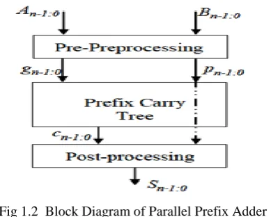
Tree-prefix algorithms include parallelism for calculation speed-up, and therefore form the category of parallel-prefix algorithms. It represents a serial algorithm for solving the prefix problemIn the prefix tree, there are n columns, corresponding to the number of input bits. The gates performing the • operation and which work in parallel are arranged in the same row, and similarly, the same gates connected in series are placed in consecutive rows. Thus, the number of rows m corresponds to the number of binary operations to be evaluated in series. The sum bits, si are finally obtained from a post processing step.
Fig 1.2 Block Diagram of Parallel Prefix Adder
Fig 1.3 Logic and symbols for Pre processing summation Gates
(1.5)
(1.6)
(1.7)
(1.4)
(1.8)
(1.9)
ISSN(Online): 2319 - 8753
ISSN (Print) :2347 - 6710
I
nternational
J
ournal of
I
nnovative
R
esearch in
S
cience,
E
ngineering and
T
echnology
(An ISO 3297: 2007 Certified Organization)
Vol. 4, Issue 2, February 2015
i i
i
A
B
G
i i i i
i
A
B
A
B
K
i i i
P
A
B
In the above equation, „.‟ operator is applied on two pairs of bits and, these bits represent generate and propagate signals used in addition. The output of the operator is a new pair of bits which is again combined using a dot operator „ ‟ or semi-dot operator „ ‟ with another pairs of bits. This procedural use of dot operator „ ‟ and semi-dot operator „ ‟ creates a prefix tree network which ultimately ends in the generation of all carry signals.In the final step, the sum bits of the adder are generated with the propagate signals of the operand bits and the preceding stage carry bit using a xor gate. Choudary(2008) proposed a new technique for basic arithmetic operation for higher automation The semi-dot operator „ ‟ will be present as last computation node in each column of the prefix graph structures, where it is essential to compute only generate term, whose value is the carry generated from that bit to the succeeding iterations
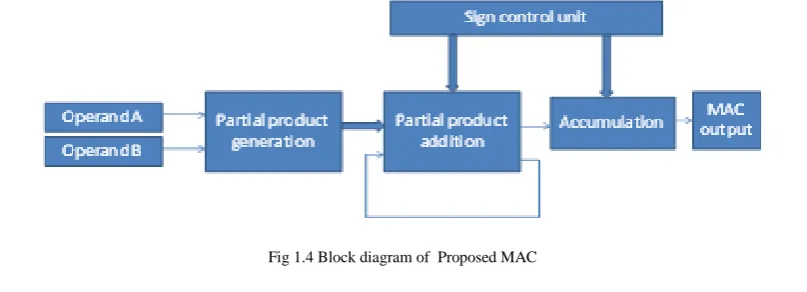
IV. MAC
The Multiply-Accumulate Unit (MAC) is the main computational kernel in DIP architectures. The MAC unit determines the power and the speed of the overall system; it always lies in the critical path. Developing high speed and low power MAC is crucial to use DSP in the future WSN. In this work, a fast and low power MAC Unit is proposed for 2D-DCT computation. Multiplication involves the generation of partial products, one for each digit in the multiplier, These partial products are then summed to produce the final product The Multiply-Accumulate Unit (MAC) is the main computational kernel in DIP architectures. The MAC unit determines the power and the speed of the overall system; it always lies in the critical path. Developing high speed and low power MAC is crucial to use DSP in the future WSN. In this work, a fast and low power MAC Unit is proposed for 2D-DCT computation. Multiplication involves the generation of partial products, one for each digit in the multiplier, These partial products are then summed to produce the final product.
Fig 1.4 Block diagram of Proposed MAC
V. MUTIPLICATION THROUGH ADDERS
Let the product register size be 16 bits. Let the multiplicand registers size be 8 bits. Store the multiplier in the least significant half of the product register. Clear the most significant half of the product register.
Repeat the following steps for 8 times:
• If the least significant bit of the product register is "1" then add the multiplicand to the most significant half of the product register.
• Shift the content of the product register one bit to the right (ignore the shifted-out bit.)
• Shift-in the carry bit into the most significant bit of the product register
(1.10)
(1.11)
(1.12)
ISSN(Online): 2319 - 8753
ISSN (Print) :2347 - 6710
I
nternational
J
ournal of
I
nnovative
R
esearch in
S
cience,
E
ngineering and
T
echnology
(An ISO 3297: 2007 Certified Organization)
Vol. 4, Issue 2, February 2015
Multiplier is the main computational kernel in DIP architectures. The Multiplier unit determines the power and the
speed of the overall system. In this work, proposed adder based on fast and low complexity Multiplier Unit is
proposed.In all DSP and image processing application Multiplier will be the basic unit. The overall performance is fully depends on Adder unit efficiency. Multiplication involves the generation of partial products, one for each digit in the multiplier, These partial products are then summed to produce the final produced.
VI. SIMULATIONS RESULTS
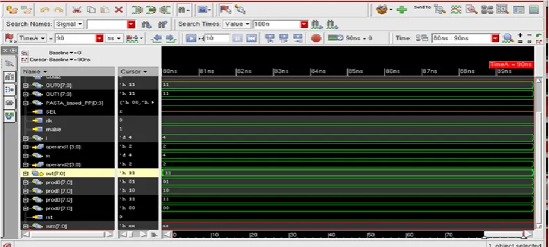
Simulations resultsSimulation output is to be obtained by using CADENCE in digital design environment.The adder was designed using multiplication technique.In this method usage the area,power consumption and time are obtained
Fig1.5Simulation for Parallel Prefix Adder
Figure 4.1 shows the simulation results of parallel prefix adder. It represents 8 bit hexadecimal values henceclock is not assigned. The timing is varied for simulation the carry and propagate values are described for each input and output values are assigned using the force operation the run time is varied for each simulation.
ISSN(Online): 2319 - 8753
ISSN (Print) :2347 - 6710
I
nternational
J
ournal of
I
nnovative
R
esearch in
S
cience,
E
ngineering and
T
echnology
(An ISO 3297: 2007 Certified Organization)
Vol. 4, Issue 2, February 2015
Figure 4.10 shows the above result is thesimulation waveform for multiplier technique using proposed adder. The clock and enable operations are performed the clock value is 0 and enable operation is 1the 4 bit are assigned multiplier technique the values are displayed in hexadecimal values the pasta pins act as a a calling function for each operation and run time for each bit is discussed the reset option is 0 the sum and carry operation performs 8 bit representation the sel act as a selection operation for input the product is multiplied using adder the each bit shifts to the previous for shift operation and hence multiplier is achieved
Fig 1.7 Area for proposed adder
ISSN(Online): 2319 - 8753
ISSN (Print) :2347 - 6710
I
nternational
J
ournal of
I
nnovative
R
esearch in
S
cience,
E
ngineering and
T
echnology
(An ISO 3297: 2007 Certified Organization)
Vol. 4, Issue 2, February 2015
Fig1.8 RTL View of Multiplier Output
Figure 1.8 shows the RTL view of multiplier output assigned with pasta blocksin the circuit the block are assigned separately for each module and pasta pins act as a calling function for each values in the multiplier technique the separate module act as a calling function for each block finally the product is assigned with each bit in the multiplier technique using multiplication through addition process the mux act as a calling function in the circuit16 bit is assigned for multiplier technique
VII. CONCLUSION
A parallel prefix adder design is proposed for overall power consumption. The proposed adder provides overall area and power than the previous methods. The parallel asynchronous self timed adder circuit is efficiently described using a handshaking protocol and also compared with other adders proposed adders. The MAC unit is implemented and the process is achieved efficiently. Simulation results demonstrate the effectiveness of the proposed framework in parallel prefix adder using multiplication through addition process. The proposed method is implemented using digital CADANCE environment
REFERENCES
[1] Brent. R.P, and Kung H.T,“Aregular layout for parallel adders”,IEEETransaction on Computer, vol. 49 C-33,volpp. 260-264.
[2] Cheng F.-C, Unger. S. H, and Theobald. M, “Self timed carry- look ahead Adders”, IEEE Transactions on Computer, vol. 49, no. 7, pp. 659–672.(2002)
[3] Choudhury.P, Sahoo.S and Chakroborty. MImplementation of basic arithmetic operations using cellular automaton”, Proceedings ofInternational centre for Information Technology, pp. 79–80.(2008)
[4] Cornelius. C, Koppe .S, and Timmermann. D “Dynamic circuit techniques in deep submicron technologies: Domino logic reconsidered”, in Proceedings of IEEEInternational conference on Integrated circuits design Technology , vol. 6, pp. 1–4.(2006)
[5] Geer.D , “Is it time for clock less chips? ”Asynchronous processor chips”, IEEE Computer., vol. 38, no. 3, pp. 18–19.(2005)
[6] Govindarajulu. S, Jayachandra Prasad. T, “Considerations of Performance Factors in CMOS Designs”, International conference on educational development, vol. 6, no. 4, pp. 554-562(2008).
[7] Kursun. V and Friedman.E.G, “Domino logic with dynamic body Biased keeper”, in Proceedings of Solid- State Circuits Conference. pp. 675–678.(2002)
ISSN(Online): 2319 - 8753
ISSN (Print) :2347 - 6710
I
nternational
J
ournal of
I
nnovative
R
esearch in
S
cience,
E
ngineering and
T
echnology
(An ISO 3297: 2007 Certified Organization)
Vol. 4, Issue 2, February 2015
[9] Lo. J.C,“A Fast Binary Adder with Conditional Carry Generation”, IEEE Transactions on Computers, vol. 46, No. 2, pp. 248-253. (1997) [10] Lynch. T, Swartz lander Jr E.E .A Spanning Tree Carry Look ahead Adder”, IEEE Transactions on Computers, vol. 41, No. 8, pp.
931-939.(1992)
[11] Martin. A.J „Asynchronous data paths and the design of asynchronous adder‟, Form. Methods vol. 19, no.4 pp. 119-137.(1992)
[12] Maezawa. M and Polonsky .S, “Dual-rail RSFQ shift register on delay-insensitive model and its applications”, Technology Representation of Institute of electronics Information and Communication Engineering, vol. 9, 97-29, pp. 19-24.(1997)
[13] Nowick. S,“Design of a low-latency asynchronous adder using speculative completion”, IEEE Proceedings of Computer Digital Technology, vol. 143, no. 5, pp. 301–307.(1996)
[14] Rahman M.Z and Klee man. L (2013), “A delay matched approach for the design of asynchronous sequential circuits”, Department of Computer System Technology International Journal on Computer vol.29, no. 6, pp. 300-310.(2013)