Available Online atwww.ijcsmc.com
International Journal of Computer Science and Mobile Computing
A Monthly Journal of Computer Science and Information Technology
ISSN 2320–088X
IJCSMC, Vol. 3, Issue. 2, February 2014, pg.181 – 186
RESEARCH ARTICLE
VLSI Implementation and Analysis of
Parallel Adders for Low Power Applications
Arunprasath S
1, Karthick A
2, Dhineshkumar D
3¹ECE & Bannari Amman Institute of Technology, Sathyamangalam ²ECE & Bannari Amman Institute of Technology, Sathyamangalam ³ECE & Bannari Amman Institute of Technology, Sathyamangalam
1
[email protected]; 2 [email protected]; 3 [email protected]
Abstract— Carry select adder (CSLA) is known to be the fastest adder among the conventional adder
structures. Due to the rapidly growing mobile industry not only the faster arithmetic unit but also less area and low power arithmetic units are needed. The modified CSLA architecture has developed using Binary to Excess-1 converter (BEC). The efficient CSLA architecture has developed using D latch. In this paper an analysis has been made between Regular and Conventional CSLA adders like modified, Efficient CSLA. Designs were developed using structural VHDL and synthesized in Altera Quartus II with reference to FPGA device EP2C35F672C6. Experimental results are compared in-terms of area, power, delay and PDP. Results shows that modified carry select adders are better in area and power consumption.
Keywords— CSLA, Adders, Low Power, VHDL, VLSI
I. INTRODUCTION
Design of area- and power-efficient high-speed data path logic systems are one of the most substantial areas of research in VLSI system design. In digital adders, the speed of addition is limited by the time required to propagate a carry through the adder. The sum for each bit position in an elementary adder is generated sequentially only after the previous bit position has been summed and a carry propagated into the next position. Area and power have major role in the designing of integrated circuit because of the increase in popularity of portable systems as well as the rapid growth of power density in VLSI circuits. Addition usually influence strongly on the overall performance of digital systems and a crucial arithmetic function. Adders are most widely used in electronic applications. For example, in microprocessors, millions of instructions per second are performed. Due to the increase in the devices like, mobile, laptop etc. Require more battery backup. Low power and area efficient addition and multiplication have always been a fundamental requirement of high performance processors and systems. Designing efficient adder is the most difficult problem for researchers in VLSI design.
© 2014, IJCSMC All Rights Reserved
182
This paper organised as follows; section II presents the detailed structure of regular CSLA. Section III and Section IV explains the modified, efficient CSLA respectively. Section V shows Results analysis, Section VI concludes our analysis.II. REGULAR 16-BIT ARCHITECTURE USING RCA [1]
In 16-bit regular carry select adder comes in the category of conditional sum adder. Conditional sum adder works on some condition. Sum and carry are calculated by assuming input carry as 1 and 0 priority the input carry comes. When actual carry input arrives, the actual calculated values of sum and carry are selected using a multiplexer. The conventional carry select adder consists of k/2 bit adder for the lower half of the bits i.e. Least significant bits and for the upper half i.e. Most significant bits (MSB's) two k/ bit adders. In MSB adders one adder assumes carry input as one for performing addition and another assumes carry input as zero. The carry out calculated from the last stage i.e. least significant bit stage is used to select the actual calculated values of output carry and sum. The selection is done by using a multiplexer.
This technique of dividing adder in stages increases the area utilization but addition operation fastens. The carry select adder comes in the category of conditional sum adder. Conditional sum adder works on some condition. Sum and carry are calculated by assuming input carry as 1 and 0 priority the input carry comes. When actual carry input arrives. The actual calculated values of sum and carry are selected using a multiplexer.
The structure of the 16-b regular CSLA is shown in Fig.1. It has five groups of different size RCA.
Fig: 1. Regular 16-bit SQRT CSLA
III.MODIFIED 16-BIT CARRY SELECT ADDER USING BEC [11]
Fig: 2 Modified 16-bit CSLA using BEC
The carry chain was further optimized by tapering down each chain stage in order to reduce the load caused by the remainder of the chain. The chain was pre-discharged at the beginning of the operation and three signals were used:The multiple-radix carry determines:
1) Whether a carry-out will be generated internally with in a section or group2.
2) whether a carry-out will be produced by a section or group2 as a result of carry being sent into the section or group2.
The modified 16-bit carry select adder circuit has Binary to excess one counter. Instead of using 2 RCA’s using one RCA and one BEC are used to reducing the circuit critical path delay. The carry propagation delay of the circuit is reduced. Because the i+1 adder didn’t depend i th carry to addition of n bits in RCA. If the mux is used selecting the either RCA or BEC depending upon previous carry value.
The area count of group 2 is determined as follows:
Gate count = 43(FA + HA + Mux + BEC) FA = 13(1*13)
HA = 6(1*6) AND = 1 NOT = 1 XOR = 10(2*5) Mux = 12(3*4).
© 2014, IJCSMC All Rights Reserved
184
Fig: 5 D-Latch Fig: 6 Input and output waveformsIV.EFFICIENT CSLA ARCHITECTURE [10]
This method replaces the BEC add one circuit by D-latch with enable signal. Latches are used to store one bit information. Their outputs are constantly affected by their inputs as long as the enable signal is asserted. In other words, when they are enabled, their content changes immediately according to their inputs. D-latch and it's waveforms are shown in Fig. 5 and Fig.6. respectively [10].
The architecture of efficient 16-b CSLA is shown in Fig.7. It has different five groups of different bit size RCA and D- Latch. Instead of using two separate adders in the regular CSLA, in this method only one adder is used to reduce the area, power consumption and delay. Each of the two additions is performed in one clock cycle.
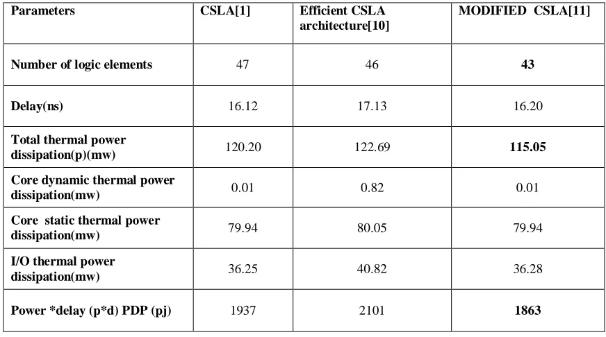
Table 1: Comparison of Area, Power, Delay and PDP.
Carry out from the previous stage i.e, least significant bit adder is used as control signal for multiplexer to select final output carry and sum of the 16-bit adder. If the actual carry input is one, then computed sum and carry latch is accessed and for carry input zero MSB adder is accessed. Cout is the output carry.
The Fig.7 shows the internal structure of group 2 of the efficient 16-bit CSLA. The group 2 performed the two bit additions which are a2 with b2 and a3 with b3. This is done by two full adder (FA) named FA2 and FA3 respectively. The third input to the full adder FA2 is the clock instead of the carry and the third input to the full adder FA3 is the carry output from FA2. The group 2 structure has three D-Latches in which two are used for store the sum2 and sum3 from FA2 and FA3 respectively and the last one is used to store carry. Multiplexer is used for selecting the actual sum and carry according to the carry is coming from the previous stage. The 6:3 multiplexer is the combination of 2:1 multiplexer.
When the clock is low a2 and b2 are added with carry is equal to zero. Because of low clock, the Latch is not enabled. When the clock is high, the addition is performed with carry is equal to one. All the D-Latches are enabled and store the sum and carry for carry is equal to one. According to the value of c1 whether it is 0 or 1, the multiplexer selected the actual sum and carry.
V. RESULTS AND DISCUSSIONS
The design were analyzed in this paper has been developed using VHDL and synthesized in Altera Quartus II with reference to FPGA device EP2C35F672C6 [7]. Area, power, Delay and PDP were the parameters is chosen for analysis. The Results shows that modified carry select adders are better in area and power consumption than [1] and [10]. Efficient CSLA provides better area than [1]. Table 1 shows the comparison between all the adders.
VI.CONCULSION
As our analysis revels that, a regular CSLA uses two copies of the carry evaluation blocks, one with block carry input is zero and other one with block carry input is one. Regular CSLA suffers from the disadvantage of occupying more chip area. The modified CSLA reduces the area and power when compared to
Parameters CSLA[1] Efficient CSLA architecture[10]
MODIFIED CSLA[11]
Number of logic elements 47 46 43
Delay(ns) 16.12 17.13 16.20
Total thermal power
dissipation(p)(mw) 120.20 122.69 115.05
Core dynamic thermal power
dissipation(mw) 0.01 0.82 0.01
Core static thermal power
dissipation(mw) 79.94 80.05 79.94
I/O thermal power
dissipation(mw) 36.25 40.82 36.28
© 2014, IJCSMC All Rights Reserved
186
REFERENCES
[1] O. J. Bedrij, “Carry-select adder,” IRE Trans. Electron. Comput., pp. 340–344, 1962.
[2] B. Ramkumar, H.M. Kittur, and P. M. Kannan, “ASIC implementation of modified faster carry save adder,” Eur. J. Sci. Res., vol. 42, no. 1, pp. 53–58, 2010.
[3] T. Y. Ceiang and M. J. Hsiao, “Carry-select adder using single ripple carry adder,” Electron. Lett., vol. 34, no. 22, pp. 2101–2103, Oct. 1998.
[4] Y. Kim and L.-S. Kim, “64-bit carry-select adder with reduced area,” Electron. Lett., vol. 37, no. 10, pp. 614–615, May 2001.
[5] J. M. Rabaey, Digtal Integrated Circuits—A Design Perspective. Upper Saddle River, NJ: Prentice-Hall, 2001.
[6] Y. He, C. H. Chang, and J. Gu, “An area efficient 64-bit square root carry-select adder for low power applications,” in Proc. IEEE Int. Symp. Circuits Syst., 2005, vol. 4, pp. 4082–4085.
[7] Quartus II user manual
[8] I. Koren, "Computer Arithmetic Algorithms", A K Peters, 2001.
[9] B. Parhami, "Computer Arithmetic: Algorithms and Hardware Designs", Oxford University Press, 2000. [10] C.S.Manikandababu “An Efficient CSLA Architecture for VLSI Hardware Implementation” IJMIE, ISSN: 2249-0558, Volume 2, Issue 5, 2012, pp.610-622.