Abstract
NOVAK, STEVEN RANDALL. Atomic Layer Deposition of Pt Nano-particles and High-k Dielectrics for Non-volatile Charge Storage Memory Devices. (Under the direction of Dr. Veena Misra).
Demand for portable non-volatile electronic memory has been the driving force behind scaling on non-volatile charge storage memory for decades. As devices continue to be aggressively scaled current technologies reach their limit of effectiveness. The use of metal nano-particles as a charge storage layer in non-volatile memory devices is a possible solution to extend the scaling of non-volatile memories; however, effective, scalable CMOS compatible nano-particle fabrication techniques are not widely available. The fabrication of metal nano-particle memory devices for application in charge storage non-volatile memory devices is discussed. A new method to grow Pt nano-particle by atomic layer deposition is developed and analyzed. The dependence of Pt nano-particle formation on growth conditions is explored, and the Pt nano-particles grown show good thermal stability as studied by rapid thermal annealing transmission electron microscopy studies in-situ.
© Copyright 2011 by Steven R. Novak
Atomic Layer Deposition of Pt Nano-particles and High-k Dielectrics for
Non-volatile Charge Storage Memory Devices
by
Steven Randall Novak
A dissertation submitted to the Graduate Faculty of
North Carolina State University
in partial fulfillment of the
requirements for the Degree of
Doctor of Philosophy
Electrical Engineering
Raleigh, North Carolina
2011
APPROVED BY:
_______________________ _______________________
Dr. Robert M. Kolbas Dr. Carlton Osburn
Biography
Acknowledgements
First and foremost the author would like to thank my advisory committee for their advice and support especially Dr. Veena Misra. This work would’ve been impossible without her guidance and foresight throughout both my undergraduate and graduate studies.
The author would also like to that my parents Paul and Joan Novak and my brother Scott for all of their endless support and encouragement over the years.
All the past and present members of Dr. Misra’s research group also deserve thanks for their contributions, collaborations, and utilization of their individual skills which contributed directly and indirectly to this work. A special thanks to Bongmook Lee for countless discussions over data, processing, research, analysis and daily coffee. Thank you to Xiangyu Yang for TEM imaging and analysis, and to Srikant Jayanti to numerous discussions about non-volatile memory device design and operation. I would also like to thank Rashmi Jha, Niv Biswas, Sriv Gowda, and Rebecca Thomas for their insight and encouragement during my time as a student. A very special thank you is due to Dan Lichtenwalner for discussions and insight on vacuum tools which on numerous occasions saved our entire group down time when tools malfunctioned.
Table of Contents
List of Figures...vi
Chapter 1: Introduction...1
1.1 Motivation...1
1.2 Charge Storage Memory...1
1.3 Flash Cell Operation...6
1.4 Flash Memory Scaling... 11
1.5 Nano-Particle Memory... 13
1.5.1 Semiconductor Nano-particle memory... 14
1.5.2 Metal Nano-particle memory... 15
1.6 Goals of the Following Work... 16
1.7 Document Preview... 17
References... 19
Chapter 2: Fabrication, Characterization, and Simulation Procedures... 23
2.1 Device Fabrication... 23
2.1.1 Metal-Oxide-Semiconductor-Capacitor Process... 23
2.1.2 Overlap Capacitors... 26
2.2 Standard Characterization Techniques... 26
2.3.1 MOSCAP... 27
2.3.2 Interfacial Trap Measurements from Conductance... 28
2.3 Memory Device Characterization... 30
2.3.1 Memory Window... 30
2.3.2 Program / Erase Time... 32
2.3.3 Retention... 34
2.3.4 P/E Cycling Reliability... 36
2.4 Physical Characterization... 38
2.4.1 SEM... 38
2.4.2 TEM... 39
2.4.3 AFM... 40
2.4.4 XPS... 41
2.5 Modeling... 42
2.5.1 General Numerical Error... 42
2.5.2 Capacitance Fitting... 43
2.5.3 Band Simulations... 43
2.5.4 Quantum Confinement Simulations... 44
2.6 Summary... 46
References... 48
Chapter 3: Metal Nano-particle Fabrication by Physical Vapor Deposition... 50
3.1 Physical Vapor Deposition Nano-particle Formation Process... 50
3.2 PVD Pt... 50
3.2.1 PVD Pt Formation on SiO2... 51
3.2.3 PVD Pt on HfO2... 59
3.2.4 Pt Nano-particle Summary... 62
3.3 PVD Ru... 62
3.3.1 PVD Ru on SiO2... 64
3.3.2 PVD Ru on Al2O3... 69
3.3.3 PVD Ru on HfO2... 71
3.4 Formation Mechanisms... 76
3.5 Problems With the PVD Method... 79
3.6 Alternative PVD Nano-particle Fabrication... 82
3.7 Summary... 84
References... 86
Chapter 4: Pt Nano-particle Fabrication by Atomic Layer Deposition... 88
4.1 Atomic Layer Deposition... 88
4.2 ALD Pt process... 92
4.2.1 ALD Pt on SiO2... 95
4.2.2 ALD Pt on Al2O3... 98
4.2.3 ALD Pt on HfO2... 102
4.2.4 ALD Pt on HF last Si... 104
4.3 ALD Pt, effect of exposure... 107
4.4 ALD Pt Temperature stability... 115
4.5 Conclusions... 118
References... 120
Chapter 5: Memory Capacitors With ALD Pt Nano-particles... 123
5.1 Device Considerations... 123
5.2 Memory Capacitors with 10 Cycles Pt ALD With 10s Exposure... 126
5.2.1 Memory Window... 127
5.2.2 Time Dependence of Programming... 134
5.2.3 Retention Characteristics... 146
5.2.4 Cycle Dependence of Memory Window... 155
5.3 Improving Charge Density (Dual Layer Pt ALD)... 161
5.4 Conclusions... 163
References... 165
Chapter 6: Conclusions and Future Work... 168
6.1 Conclusions... 168
6.2 Future Work... 171
6.2.1 Dielectric Optimization... 171
6.2.2 Memory Device Fabrication... 172
6.2.3 Selective Deposition by Chemical Patterning... 173
List of Figures
INTRODUCTION
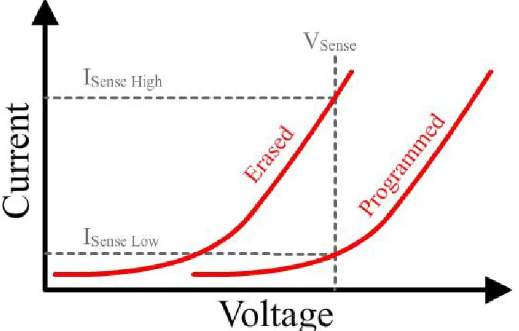
Figure 1 Current versus voltage relation ship of a floating gate
transistor………..2
Figure 2 Cross sectional drawing of a NOR flash array……… 4
Figure 3 Cross-sectional drawing of a NAND flash array……… 6
Figure 4 Standard flash memory device……….. 7
Figure 5 Schematic drawing of different program techniques for flash devices………... 8
Figure 6 : Circuit model schematic for MOSFET and MOSCAP coupling factors………10
FABRICATION, CHARACTERIZATION, AND SIMULATION PROCEDURES Figure 1 Step by step overview of MOS capacitor fabrication process………...24
Figure 2 Schematic illustrating the structure of overlap and non-overlap MOS capacitors………. 25
Figure 3 Circuit model for Dit measurement on MOS capacitors………... 29
Figure 4 High frequency CV curves and applied biases for memory window measurements………31
Figure 5 Ideal representation of the separation between stress and sense areas…….. 33
Figure 6 Voltage versus time waveforms illustration for program / erase time measurements………34
Figure 7 Voltage versus time waveforms illustration for retention measurements…. 35 Figure 8 Voltage versus time waveforms illustration for program and erase cycling measurements………37
Figure 9 Representations of nano-particle for quantum simulations………... 45
METAL NANO-PARTICLE FABRICATION BY PHYSICAL VAPOR DEPOSITION Figure 1 Illustration of PVD nano-particle formation………. 51
Figure 2 SEM image of 2 nm Pt on SiO2 after anneal………. 52
Figure 3 Extracted histogram of particle diameter for 2 nm Pt on SiO2……….. 52
Figure 4 SEM image of 4 nm Pt on SiO2 after anneal………. 53
Figure 5 Extracted histogram of particle diameter for 4 nm Pt on SiO2………. 54
Figure 6 SEM image of 6 nm Pt on SiO2 after anneal………. 55
Figure 7 Plots of Pt particle size and Density on SiO2 versus film deposition thickness………55
Figure 8 SEM image of 2 nm Pt on Al2O3 after anneal………... 56
Figure 9 Extracted histogram of particle diameter for 2 nm Pt on Al2O3……… 57
Figure 11 SEM image of 6 nm Pt on Al2O3 after anneal………. 59
Figure 12 SEM image of 2 nm Pt on HfO2 after anneal……….…. 60
Figure 13 Histogram of particle diameter for 2 nm Pt on HfO2……….. 60
Figure 14 SEM image of 4 nm Pt on HfO2 after anneal………. .61
Figure 15 SEM image of 6 nm Pt on HfO2 after anneal……….. 61
Figure 16 SEM image of 2 nm Ru on SiO2 after anneal………..63
Figure 17 SEM image of 4 nm Ru on SiO2 after anneal………..63
Figure 18 Histogram of particle diameter for 4 nm Pt on SiO2………... 64
Figure 19 SEM image of 6nm Ru on SiO2 after anneal………...65
Figure 20 Histogram of particle diameter for 6nm Ru on SiO2………... 65
Figure 21 Plots of Ru particle diameter and density versus deposition thickness on SiO2………... 66
Figure 22 SEM image of 2 nm Ru on Al2O3 after anneal………67
Figure 23 Histogram of particle diameter for 2 nm Ru on Al2O3……… 68
Figure 24 SEM image of 4 nm Ru on Al2O3 after anneal………68
Figure 25 Histogram of particle diameters for 4 nm Ru on Al2O3……….. 69
Figure 26 SEM image of 6 nm Ru on Al2O3 after anneal………70
Figure 27 Plots of particle diameter and density for Ru on Al2O3………...70
Figure 28 SEM image of 2 nm Ru on HfO2 after anneal………. 71
Figure 29 Histogram of particle diameters for 2 nm Ru on HfO2………... 72
Figure 30 SEM image of 4 nm Ru on HfO2 after anneal………. 72
Figure 31 Histogram of particle diameters for 4 nm Ru on HfO2………... 73
Figure 32 SEM image for 6 nm Ru on HfO2 after anneal……… 73
Figure 33 Histogram of particle diameters for 6nm Ru on HfO2……… 74
Figure 34 Plots of particle size and density versus film thickness for Ru on HfO2….75 Figure 35 Theoretical calculation of maximum possible particle densities as a function of particle spacing and radius in a hexagonal lattice……….. 79
Figure 36 Plots of ground state energy perturbations and Coulombic charging energy as a function of nano-particle size……… 80
Figure 37 Electrical data from PVD Pt nano-particle memory.………...83
PT NANO-PARTICLE FABRICATION BY ATOMIC LAYER DEPOSITION Figure 1 Schematic drawing of the ALD deposition of Al2O3 by TMA and H2O... 89
Figure 2 Schematic drawing of the Pt ALD... 93
Figure 3 QCM measurements of ALD Pt thickness and growth rate... 95
Figure 4 AFM images of Pt ALD on SiO2... 96
Figure 5 Plots of ALD Pt nano-particle size and RMS roughness on SiO2... 96
Figure 6 Pt 4f signal from XPS for Pt on SiO2... 97
Figure 7 AFM images of Pt ALD on Al2O3... 99
Figure 8 Plots of ALD Pt nano-particle size and RMS roughness on Al2O3... 100
Figure 9 Pt 4f XPS signal as a function of Pt ALD cycles on Al2O3... 101
Figure 10 AFM images of Pt ALD on HfO2... 102
Figure 11 RMS roughness of Pt ALD on HfO2... 103
Figure 13 200 cycles ALD Pt on SiO2, Al2O3, HfO2 and H terminated Si... 105
Figure 14 TEM image of 35 cycles ALD Pt on Al2O3... 108
Figure 15 Histogram of Pt ALD nano-particle diameters and probability density ... 109
Figure 16 35 cycles of ALD Pt with no exposure, 10s exposure and 20s exposure . 112 Figure 17 TEM showing the effect of reducing the cycle count while using exposure during the Pt ALD process ... 113
Figure 18 Histogram of ALD Pt nano-particle diameters using precursor exposure and probability density as a function ... 114
Figure 19 Comparison of the particle density calculated from TEM and the maximum theoretical particle density... 115
Figure 20 In-situ TEM annealing studies for ALD Pt nano-particles embedded in Al2O3. ... 116
Figure 21 Plots of average particle size and particle density for ALD Pt nano-particles as a function of temperature ... 117
MEMORY CAPACITORS WITH ALD PT NANO-PARTICLES Figure 1 Calculations showing the relationship and tradeoffs between TOX and IPD thicknesses and dielectric constants……… 123
Figure 2 Cross sectional schematic of Pt nano-particle memory device, memory control device and single layer control device………125
Figure 3 Memory windows obtained by the hysteresis method for memory control samples and Pt nano-particle memory samples……….. 127
Figure 4 Charging and leakage comparison for single layer control samples……... 128
Figure 5 Band simulations of single layer and memory control with HfO2 IPD…... 129
Figure 6 Corrected memory window plots showing the charging effect of ALD Pt nano-particles with Al2O3 IPD and HfO2 IPD……… 130
Figure 7 Calculated ALD Pt nano-particle charge densities for both Al2O3 and HfO2 IPD layers………132
Figure 8 Charging as a function of time for memory control device and Pt nano-particle memory device with Al2O3 IPD……….133
Figure 9 The effects Pt nano-particle charging when corrected for Al2O3 charging. 134 Figure 10 Charging as a function of time for memory control device and Pt nano-particle memory device with HfO2 IPD………..135
Figure 11 The effects Pt nano-particle charging when corrected for HfO2 charging 136 Figure 12 Dit measurements by the conductance method show an increase in Dit with increasing time constant………..137
Figure 13 Band simulations of Pt memory device………. 140
Figure 14 Leakage current plots for Al2O3 single layer controls………... 142
Figure 15 : Leakage current plots for HfO2 single layer controls……….. 143
Figure 16 Leakage current plots for SiO2 single layer controls………. 144
Figure 17 Long term retention measurements from memory control samples with Al2O3 IPD………... 145
Figure 19 Long term retention measurements from memory control samples with
HfO2 IPD……….148
Figure 20 Long term retention measurements from Pt nano-particle memory samples
with HfO2 IPD……….149
Figure 21 P/E Cycling for Al2O3 IPD memory controls……… 154
Figure 22 P/E Cycling for Al2O3 IPD Pt nano-particle memory devices………….. 155
Figure 23 P/E Cycling for HfO2 IPD memory controls………. 156
Figure 24 P/E Cycling for HfO2 IPD Pt nano-particle memory devices…………... 157
Figure 25 Comparison of memory window for memory control, single ALD Pt nano-particle layer, and dual ALD Pt nano-nano-particle layer devices……….. 160 Figure 26 Charge density plots for single and dual Pt nano-particle charge trap layers
Chapter 1: Introduction
1.1 Motivation
The increasing popularity and availability of portable electronic devices, such as Smart Phones, netbooks, and personal media players, have created an insatiable demand for fast, dense, and low power non-volatile memory. This demand is primarily filled by a specific electronically erasable programmable read only memory (EEPROM) known as flash memory. Reflecting this demand, the NAND flash market alone saw a 34% increase in revenue to $18 billion from 2009 to 2010 [1]. With an increasing variety of new and innovative portable electronic devices reaching the market, demand for flash memory is on the rise as well as the demand for smaller, quicker and lower power devices. But continuing to reduce the size and power consumption of flash memory devices in order to satisfy the demand is becoming increasingly more difficult, and traditional methods to scale flash devices are approaching their limits. In order to continue the trends in flash device scaling, research into new materials and modified devices geometries is needed and this is currently an active area of semiconductor device research.
1.2 Charge Storage Memory
memory and its predecessors, Electronically Programmable Read Only Memory (EPROM) and EEPROMs, accomplish all of the aforementioned stipulations by trapping or storing charge close to the channel of a MOSFET. The presence or absence of this charge near the channel of a MOSFET, alters the Flatband voltage (VFB) and hence the threshold voltage
(VT) of the device. This leads to differences in drain current between the two (or more)
different thresholds that varies by many orders of magnitude for a given gate bias (Fig 1.1). These two (or more ) current levels can be detected with a sense amp, and if the charge near the channel doesn’t leak away after the system is removed from a power source, the device will fill the basic requirements for a non-volatile memory device.
Although there were functional charge trapping memory devices reported earlier [2], practical EPROM devices were first reported in 1971 [3]. The floating gate avalanche
injection metal oxide semiconductor (FAMOS) device, as it was called, resembles a MOS transistor with its gate completely embedded in oxide with no external electrical contact. Charge was put onto the floating gate by inducing avalanche breakdown of either the source or drain junctions resulting in a current through the oxide [4]. To allow selective reads and writes, each FAMOS device was paired with a select transistor, making FAMOS technology a 2 transistor (2T) cell. Once charged, the floating gate had no discharge path and the device retained its new threshold. Erasing was accomplished by externally applying UV light for 10 ~ 20 minutes. The UV photons would be absorbed by the trapped electrons, giving them the energy needed to overcome the SiO2 barrier and tunnel back to the substrate. This design
gave an advantage over masked read only memory (ROM) and fuse programmable read only memory (PROM) in that changes to data stored in the memory could be implemented by the end user. However, the need to expose the memory chips to UV light required packaging that had a quartz window above the chip; an added expense to the manufacturing process. Additionally, the presence of the window, if not properly covered, could lead to unintended erasures.
EEPROM devices emerged in the 1980’s with the floating gate tunnel oxide (FLOTOX) device [6]. In this device charge is tunneled onto the floating gate by Fowler-Nordheim (FN) tunneling, creating the programmed state. Charge is removed from the floating gate also by FN tunneling which not only allows in-system electrical erasures, but also reduces erase times from 10 minutes to 10 ms. The downside to FLOTOX memories was that a 2T cell was needed to isolate memory cells during writes, effectively reducing the maximum bit density possible.
Although variations in current memory technologies exist, the general flash memory cell is very similar to FLOTOX EEPROM memories devices particularly in the cell structure and operation. The difference is in how they are arranged to take advantage of semiconductor real estate. Flash devices are arranged in blocks of memory on the die to share common read,
write, and erase circuitry. This gives an advantage over EEPROM in reducing the needed chip area, but at the cost of the ability to write individual bytes. Although there are many physical implementations of flash memory cells, there are two basic cell arrangements, NOR and NAND.
In the NOR cell (Fig. 1.2), memory transistors are arranged so that columns share a metal line with contacts to the drains of the transistors in the columns. Rows of memory transistors also share common diffused sources, where contacts are not needed since the source is common to all devices. This arrangement allows for fast random reads, since each device has direct contact to the bit lines through the drain. Because of the fast random access ability of NOR flash, it finds the most applications in memory for program storage, or mixed program and data memory. The fast random access speed gets rid of the need to copy program instructions from non-volatile memory into RAM, and programs can be ran directly from NOR flash.
extensively in applications where large amounts of sequential data are needed, such as digital audio, video, and photos.
1.3 Flash Cell Operation
Memory cells need to be reliably programmed and erased and their state correctly determined for proper operation. The basic flash memory cell, as described above, is shown in figure 1.4. The device resembles a typical metal oxide semiconductor (MOS) transistor, except for the presence of a floating gate in the gate stack. This floating gate makes up the charge storage layer in flash memory devices and historically has been made of polycrystalline-silicon (poly) and sometimes Si3N4. The floating gate is completely
embedded in non-conducting oxide layer (typically SiO2) so once charge is placed on the
floating gate, it cannot leak away.
It is well know that the turn on voltage (VT) is proportional to fixed oxide charge and is
represented by equation (1.1)[8]:
(
0 0)
0+γ +φ − φ
= T CB
T V V
V (1.1)
where
0 0
0 0
0
0 =φ − +φ +γ φ = FB +φ +γ φ OX
MS
T V
C Q
V (1.2)
Here φMS is the difference in metal and semiconductor workfunctions, Q0 is the effective
oxide interface fixed charge, COX is the oxide capacitance, γ is the body factor, φ0 is the
approximate semiconductor potential in strong inversion, and VFB is the flatband voltage. In a
flash device, charge trapped on the floating gate can be modeled as an effective Q0, and the
electric field created by the charge, couples with the transistor channel causing the apparent threshold shift. The equation for this threshold shift can be simplified from (1.1) and (1.2) giving:
Substrate
Control Gate
Inter-Poly / Control Dielectric
Floating Gate
Tunnel Dielectric
Substrate
Control Gate
Inter-Poly / Control Dielectric
Floating Gate
Tunnel Dielectric
OX OX trapped
OX trapped
T t
Q
C Q V
ε
− = −
=
∆ (1.3)
Here εox and tox are the permittivity and thickness respectively of the oxide between the
floating gate and control gate. Since the floating gate and control gate are typically both made of poly, this dielectric is often referred to as the inter-poly dielectric (IPD). Some modern memory devices may stray away from using poly, and therefore the IPD is sometimes also referred to as the blocking oxide however is this work we will refer to this oxide as an IPD, whether there is or is not poly present in the device stack.
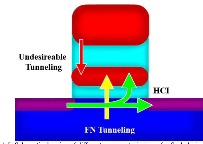
Programming and erasing of devices is achieved by tunneling electrons through the bottom oxide, aptly referred to as the tunnel oxide. Figure 1.5 illustrates the two main methods for programming flash memory devices, hot carrier injection (HCI) and FN tunneling, as well as the unwanted tunneling that occurs through the IPD.
Figure 1.5: Schematic drawing of different program techniques for flash devices. Both hot carrier and Fowler-Nordheim tunneling are shown as well as undesireable
To program a device using HCI, a moderate bias is placed on the control gate (~5V) and a large bias is placed from source to drain (10~15V) causing a high drain to source current through the channel of the device and a high electric field at the drain. The high field causes impact ionization and creates high energy carriers (hot carriers), and a few of them will have enough energy to overcome the Si-SiO2 barrier and tunnel into the floating gate.
The lowered electron injection barrier allows more electrons to tunnel towards the gate. The advantage of device programming by HCI, is that programming times are low, devices can be programmed quickly, and it is possible to locally inject charge into a floating gate since the high energy carriers are closer to the drain side of the device where the field is highest. The disadvantages are that high voltage and currents are needed to produce hot carriers meaning power consumption is high and that carriers can get trapped in the oxide during tunneling and create permanent charge that can shift threshold voltages and increase oxide leakages.
Programming devices with FN tunneling is achieved by applying a large bias across the tunnel oxide, causing a large amount of band bending in the oxide. This effectively changes the shape of the potential barrier from a trapezoid to a triangle and lowers the effective barrier width allowing electrons to tunnel though the oxide. This form of programming is advantageous because it is a low power process, and electrons can tunnel uniformly across the device. The disadvantages of FN programming are that it is a slower programming process and also subjects the gate oxide to repeated high field stress which can increase the leakage over time and repeated programming.
Additionally, these devices can be erased with UV light exposure, but modern devices are not packaged to allow this.
To program and / or erase flash memory devices by FN tunneling, it is desirable to have as much as possible of the applied gate stack bias to be dropped across the tunnel oxide. This ensures the lowest possible programming voltages, and hence programming power, as well as minimizing unwanted tunneling through the IPD. Figure 1.6 shows a schematic of a floating gate MOSFET (a) and MOSCAP (b). The potential on the floating gate for the MOSFET, can be expressed as [9]:
T D T D C T C F
C Q V C C V C C
V = + + (1.4)
where CC is the IPD capacitance, CD is the drain capacitance, and CT is the total capacitance.
From (1.4) we can call the coupling factor:
Source Body Drain
Control Gate
Cc
CD
CB
CS
Body Control Gate
Cc
CB
MOSFET
MOS-Cap
FG
FG
Source Body Drain
Control Gate
Cc
CD
CB
CS
Body Control Gate
Cc
CB
MOSFET
MOS-Cap
FG
FG
T C C
C C =
α (1.5)
which can be thought of as the percent of total bias that appears on the floating gate. The ideal coupling factor of a memory device is 1, which occurs when the tunnel oxide capacitance is zero. This situation is not practical for memory devices because of the absence of the tunnel oxide. There are a number of tradeoffs when considering coupling factors and a handful of possible ways to optimize them as well. These methods and considerations are discussed in more detail in chapter 5.
1.4 Flash Memory Scaling
To achieve higher bit densities and therefore lower costs per bit, flash devices are scaled down in size, allowing more devices to be fabricated in a given semiconductor area. However, the scaling of flash devices is not a trivial task. Although certain technologies can be adapted from conventional CMOS logic scaling, the need for extremely low leakage dielectrics (< 5x10-25 A/cm2 for the 32 nm node) [10] that can hold up to repeated high voltage stressing during programming and erase (>10,000 cycles for 32 nm node) [10] places great constraints on the dielectric chosen and creates immense challenges to continued scaling.
an increase in gate leakage by direct tunneling for MOS devices that cannot be tolerated in memory devices if they are to meet the 10 year retention standard. This puts a lower limit on the scalability of SiO2 as the tunnel oxide for memory devices, typically in the 5 ~ 7nm range
[11].
IPD scaling, however, is not as limited as tunnel oxide scaling, and is a primary way to regain channel control in scaled memory devices. However, scaling the IPD thickness leads to a reduction in coupling factor by decreasing the IPD capacitance with respect to the tunnel oxide capacitance. Traditionally, this was compensated for by overlapping the control gate around the floating gate [5][12]. This technique works by increasing the control gate to FG area, and hence the IPD capacitance, while keeping the same FG to channel area. However as device pitches are scaled down the parasitic device to device capacitance increases leading to read and write disturbs between cells. Eventually it is no longer advantageous to overlap the sides of the FG, and alternate paths to scaling while maintaining good coupling between the control and floating gate are needed.
devices have improved the behavior of some flash memory device structures, it is generally agreed that SONOS will not scale down past the 35nm node [10].
1.5 Nano-Particle Memory
Although SONOS itself has limitations, the discrete nature of SONOS trapping layers is still attractive for device scaling. As flash devices are scaled down, tunnel oxides need to be scaled as well. But as oxide thicknesses are scaled, the random variation in thickness during the growth process becomes increasingly significant. These random deviations in thickness result in localized defects in the tunnel oxide and can create conductive paths from the floating gate to the substrate [17]. For a floating gate mode of a continuous conducting layer, a single defect in the device’s tunnel oxide could discharge the entire charge storage layer and create a failed flash transistor. However if the charge storage layer is made of discrete traps, then only the charge stored near the defect will be lost due to the increases oxide conduction and a lower percent of devices will fail. In SONOS memories the trap layer is continuous although the traps themselves are discrete. This allows for lateral charge movement through the SiN film and can in turn discharge the entire layer [18] , albeit slower then a continuous conducting layer.
additional barrier can reduce the lateral charge hopping as observed in SiN films and improve retention [20]. There also exists a large variety of materials which NPs can be made from allowing for extra flexibility in memory device design by tuning material or deposition parameters.
1.5.1Semiconductor Nano-particle memory
A wide variety of nano-particles made from semiconductors have been examined as charge storage layers [21][22][23]. Most semiconductors can withstand standard CMOS processing and semiconductor nano-particles can be deposited or formed by CMOS compatible processes such as chemical vapor deposition (CVD) [24][25], implantation [26], or physical vapor deposition (PVD) [27]. Initial results with semiconducting nano-particles show that enhancement in write / erase speeds [28] and lower voltages [29] are obtained compared to conventional floating gate memories. However these advantages seemingly come at the cost of low memory windows and poor long-term retention. It has been theoretically calculated that for Si nano-crystals the lowest energy state will sit at or above the substrate conduction band [30]. The positioning of electron energy levels in the nano-crystal would predict little to no retention in semiconductor nano-particle based memories. The retentions observed are slightly better then predicted, and it is theorized that the improvement stems from deep level traps in the Si nano-particle [31].
quantization of electrical states. This effect is clearly observed as device to device variations in the VT across wafers and the variation is more pronounced as the device dimensions
decrease [32]. Furthermore it is well known that the random variations in the number and position of dopants in a Si channel region leads to VT variations and hence Fermi level
variations [33]. The problem is worse as the Si area is decreased and fewer numbers of dopants are needed to achieve the same doping level. In a semiconductor nano-particle, this problem can lead to variations in retention across the wafer as the band alignment between individual devices and the substrate varies. Even for intrinsic semiconductor NPs, this effect still plays a role because it is extremely hard to remove all unwanted contaminants during processing.
1.5.2Metal Nano-particle memory
Many of the short comings of semiconductor nano-particles are not predicted to occur when metal nano-particles are used; yet most of the advantages observed by using semiconductor nano-particles are preserved. For instance, the same discrete charge storage behavior as well as evidence of the Coulomb blockade effect is seen with metal nano-particles [34]. The high free electron densities in metals reduce the impact of Fermi level variation due to random dopant and / or contaminant fluctuations as well as allow for higher charge storage capacities. The absence of a bandgap in metals reduces the impact of quantum confinement, which allows for better retention over semiconducting nano-particles. The reduced sensitivity to quantum confinement also leads to less variation of VT shifts with
there exist a large variety of metals with a range of work functions allowing for tuning of the nano-particle energy level to allow a charged state aligning within the substrate bandgap and the discharged state outside the band gap which would give optimal program / erase and retention characteristics.
Metal nano-particles have been fabricated by some of the same methods as previously mentioned for semiconducting nano-particles [35][36], as well as colloidal and organic solution based methods [37]. A popular method for metal nano-particle formation is to deposit a thin metal wetting layer, typically a few nanometers thick and then rapid thermal annealing (RTA) the thin film at high temperature to reduce the surface free energy of the system by the process of agglomeration, increase surface mobility, and cause the formation of NPs [38]. This wet and anneal method has its own set of merits and limitations which will be discussed in detail in chapter 3.
Metal nano-particle based flash memory has the potential to overcome the known and expected problems in future memory technologies and to allow the continued scaling in the sub-100nm regime. However technical challenges still exist and there is still a significant amount of research to be done on metal nano-particles before their used in memories is widespread.
1.6 Goals of the Following Work
nano-particles can be deposited over a long range, conformally, reliably, and compliant with current CMOS processes. One specific property needed to be compatible with current CMOS processing techniques is that the metal nano-particles must be able to withstand thermal budgets high enough to activate dopants (900oC ~ 1000oC). Additionally the process needs to be scalable across multiple technology nodes.
1.7 Document Preview
This chapter (chapter 1) has been an introduction and brief history of the development of charge storage, especially flash, memory devices as well as considerations for device scaling, limitations, and the advantages of using metal nano-particle memories.
Chapter 2 describes the fabrication and characterization techniques that are used pervasively throughout this work.
Chapter 3 documents the work done to form high workfunction metal nano-particles by the annealing of thin metal films deposited by PVD. Further more possible mechanisms which affect the formation of metal nano-particles by this method are discussed as well as the undesirable aspects observed.
Chapter 4 describes the development of a Pt nano-particle deposition technique by atomic layer deposition (ALD) and parameters which can be tuned to alter the growth of the Pt particles. Furthermore, this technique is compared to the deposition technique described in chapter 3 and any advantages of the ALD method are determined.
used and compared and the prospect of Pt ALD nano-particles for future scaling of memory devices is discussed.
References
[1] “NAND Flash Revenue Rising to $18 Billion in 2010, Up 34% From 2009,”
StorageNewsletter.com, 17-Feb-2010.
[2] D. Frohman-Bentchkowsky, “The metal-nitride-oxide-silicon (m.n.o.s.) transistor- characteristics and applications,” Proceedings of the IEEE, vol. 58, no. 8, pp. 1207-19, 1970.
[3] D. Frohmann-Bentchkowsky, “A fully-decoded 2048-bit electrically-programmable MOS-ROM,” in Digest of technical papers of the 1971 international solid state circuits
conference, 17-19 Feb. 1971, pp. 80-1, 1971.
[4] E. H. Nicollian, “Avalanche Injection Currents and Charging Phenomena in Thermal SiO2,” Applied Physics Letters, vol. 15, no. 6, p. 174, 1969.
[5] P. Salsbury, W. Morgan, G. Perlegos, and R. Simko, “High performance MOS EPROMs using a stacked-gate cell,” in 1977 International Solid-State Circuits
Conference. (Digest of Technical Papers), 16-18 Feb. 1977, pp. 186-7, 1977.
[6] W. Johnson, G. Perlegos, A. Renninger, G. Kuhn, and T. Ranganath, “A 16Kb electrically erasable nonvolatile memory,” in 1980 IEEE International Solid-State
Circuits Conference Digest of Technical Papers, 13-15 Feb. 1980, pp. 152-3, 1980.
[7] F. Masuoka, M. Momodomi, Y. Iwata, and R. Shirota, “New ultra high density EPROM and flash EEPROM with NAND structure cell,” in 1987 International Electron Devices
Meeting, IEDM. Technical Digeset (Cat. No.87CH2515-5), 6-9 Dec. 1987, pp. 552-5,
1987.
[8] Y. Tsividis, Operation and Modeling of the MOS Transistor, 2nd ed. Oxford University Press, USA, 2003.
[9] P. Cappelletti, C. Golla, P. Olivo, and E. Zanoni, Flash Memories, 1st ed. Springer, 1999.
[10] “2009 ITRS.” [Online]. Available: http://www.itrs.net/. [Accessed: 26-Jul-2010]. [11] H. Heinisch, “Interpoly Oxide for Floating Gate Memory Devices Fabricated by Rapid
[12] R. Muller, H. Nietsch, B. Rossler, and E. Wolter, “An 8192-bit electrically alterable ROM employing a one-transistor cell with floating gate,” Solid-State Circuits, IEEE
Journal of, vol. 12, no. 5, pp. 507-514, 1977.
[13] T. Chang et al., “Oxidized-nitridized oxide (ONO) for high performance EEPROMS,”
in International Electron Devices Meeting. Technical Digest, 13-15 Dec. 1982, p. 810,
1982.
[14] S. Mori et al., “Reliability study of thin inter-poly dielectrics for non-volatile memory application,” in Reliability Physics Symposium, 1990. 28th Annual Proceedings.,
International, pp. 132-144, 1990.
[15] P. Chen, “Threshold-alterable Si-gate MOS devices,” IEEE Transactions on Electron
Devices, vol. 24, no. 5, pp. 584-6, May. 1977.
[16] B. Eitan, P. Pavan, I. Bloom, E. Aloni, A. Frommer, and D. Finzi, “NROM: A novel localized trapping, 2-bit nonvolatile memory cell,” Electron Device Letters, IEEE, vol. 21, no. 11, pp. 543-545, 2000.
[17] O. Ginez, J. Daga, P. Girard, C. Landrault, S. Pravossoudovitch, and A. Virazel, “Retention and Reliability Problems in Embedded Flash Memories: Analysis and Test of Defective 2T-FLOTOX Tunnel Window,” in VLSI Test Symposium, 2007. 25th IEEE, pp. 47-52, 2007.
[18] E. Lusky, Y. Shacham-Diamand, I. Bloom, and B. Eitan, “Electrons retention model for localized charge in oxide-nitride-oxide (ONO) dielectric,” Electron Device Letters, IEEE, vol. 23, no. 9, pp. 556-558, 2002.
[19] Liangcai Wu et al., “Charging and Coulomb blockade effects in nanocrystalline Si dots embedded in SiO2 matrix,” in Solid-State and Integrated Circuits Technology, 2004.
Proceedings. 7th International Conference on, vol. 2, pp. 898-901 vol.2, 2004.
[20] J. De Blauwe, “Nanocrystal nonvolatile memory devices,” Nanotechnology, IEEE
Transactions on, vol. 1, no. 1, pp. 72-77, 2002.
[21] Tae Hee Lek, Dong Uk Lek, Seon Pil KlM, and Eun Kyu Kim, “Electrical
characterization of nano-floating gate capacitor with silicon carbide nano particles,”
Japanese Journal of Applied Physics, vol. 47, no. 6, pp. 4992-5, Jun. 2008.
[22] S. Tiwari, F. Rana, K. Chan, H. Hanafi, Wei Chan, and D. Buchanan, “Volatile and non-volatile memories in silicon with nano-crystal storage,” in Electron Devices
[23] Ya-Chin King, Tsu-Jae King, and Chenming Hu, “Charge-trap memory device
fabricated by oxidation of Si1-x Gex,” Electron Devices, IEEE Transactions on, vol. 48,
no. 4, pp. 696-700, 2001.
[24] C. Gerardi, B. DeSalvo, S. Lombardo, and T. Baron, “Performances of Si nanocrystal memories obtained by by CVD and their potentialities to further scaling of non-volatile memories,” in Integrated Circuit Design and Technology, 2004. ICICDT '04.
International Conference on, pp. 37-43, 2004.
[25] S. Iwashita, H. Miyahara, K. Koga, M. Shiratani, S. Nunomura, and M. Kondo, “Plasma CVD for Producing Si Quantum Dot Films,” in Discharges and Electrical Insulation in
Vacuum, 2006. ISDEIV '06. International Symposium on, vol. 2, pp. 558-560, 2006.
[26] H. Hanafi and S. Tiwari, “A controlled threshold low power nano-crystal memory,” in
Proceedings of 25th European Solid State Device Research Conference, 25-27 Sept. 1995, pp. 209-12, 1995.
[27] M. Bernardi, A. Sgarlata, N. Motta, M. Fanfoni, D. Del Moro, and A. Balzarotti, “Ordering of Ge quantum dots on silicon surfaces via bottom-up and top-down approaches,” in Nanoscience and Nanotechnology, 2008. ICONN 2008. International
Conference on, pp. 148-151, 2008.
[28] H. Hanafi, S. Tiwari, and I. Khan, “Fast and long retention-time nano-crystal memory,”
IEEE Transactions on Electron Devices, vol. 43, no. 9, pp. 1553-8, Sep. 1996.
[29] Kwangseok Han, Ilgweon Kim, and Hyungcheol Shin, “Characteristics of P-channel Si nano-crystal memory,” in TENCON 99. Proceedings of the IEEE Region 10
Conference, vol. 2, pp. 1140-1142 vol.2, 1999.
[30] S. Tiwari, F. Rana, K. Chan, Leathen Shi, and H. Hanafi, “Single charge and
confinement effects in nano-crystal memories,” Applied Physics Letters, vol. 69, no. 9, pp. 1232-4, 1996.
[31] Y. Shi et al., “Silicon nano-crystals based MOS memory and effects of traps on charge storage characteristics,” in Proceedings of Fifth International Conference on Solid-State
and Integrated Circuit Technology-ICSICT'98, 21-23 Oct. 1998, pp. 838-41, 1998.
[32] E. Nagata, N. Takahashi, H. Ishikuro, and T. Hiramoto, “Characteristics distribution of narrow channel MOSFET memories with silicon nano-crystal floating gates,” in Digest of Papers. Microprocesses and Nanotechnology '99. 1999 International Microprocesses
[33] Y. Yasuda, M. Takamiya, and T. Hiramoto, “Threshold voltage fluctuations induced by statistical `position' and `number' impurity fluctuations in bulk MOSFETs,” in 5th
Silicon Nanoelectronics Workshop, 11-12 June 2000, vol. 28, pp. 357-61, 2000.
[34] S. F. Hu, R. L. Yeh, and R. S. Liu, “Formation mechanism and Coulomb blockade effect in self-assembled gold quantum dots,” Journal of Vacuum Science & Technology
B: Microelectronics and Nanometer Structures, 2004. [Online]. Available:
10.1116/1.1633774. [Accessed: 27-Jul-2010].
[35] Kyoung-sik Moon, Hai Dong, S. Pothukuchi, Yi Li, and C. Wong, “Nano metal particles for low temperature interconnect technology,” in Electronic Components and
Technology Conference, 2004. Proceedings. 54th, vol. 2, pp. 1983-1988 Vol.2, 2004.
[36] A. Pavel, P. Kirawanich, R. Ravindran, S. Gangopadhyay, and N. Islam, “Effect of Incorporating Metal nanoparticles in High-k Dielectrics for NanoFLASH and NanoCMOS,” in Region 5 Technical Conference, 2007 IEEE, pp. 25-28, 2007. [37] K. Okuyama, W. Lenggoro, and T. Iwaki, “Nanoparticle Preparation and Its
Application — A Nanotechnology Particle Project in Japan,” in MEMS, NANO and
Smart Systems, 2004. ICMENS 2004. Proceedings. 2004 International Conference on,
pp. 369-372, 2004.
Chapter 2: Fabrication, Characterization, and Simulation Procedures
2.1 Device Fabrication
2.1.1 Metal-Oxide-Semiconductor-Capacitor Process
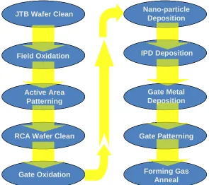
The heart of any metal oxide semiconductor (MOS) transistor is the capacitor made between the gate electrode and the substrate, and there is a wealth of information that can be determined from the fabrication of this MOS capacitor (MOSCAP). A major advantage of this structure is that its fabrication is only a fraction of a complete MOS field effect transistor MOSFET process and hence much less costly and complex. Therefore preliminary experiments can be carried out quicker and cheaper then if every device were to use a MOSFET. As much as is possible, the MOSCAP process mirrors the MOSFET process to minimize the differences between the MOSCAPs and what would be the final MOSFETs. An overview of the MOSCAP process flow is given in figure 2.1.
Device isolation is obtained by a field oxide (FOX) process. P-type or N-type silicon wafers with (100) orientation are given a JTB-100 clean to remove any surface contaminates [1]. A 2700Å FOX is then grown by wet oxidation for 30 minutes at 1000oC in an O2 / H2 /
HCl / N2 environment [2]. The active device area is patterned from the isolating FOX with
the RCA clean and is removed by a 30s dip in 1% HF acid. Gate oxides are then grown by thermal oxidation of the silicon substrate in dry O2 / HCl / N2 environment.
Floating gate layers are deposited on top of the gate oxide layer by either physical vapor deposition (PVD) or atomic layer deposition (ALD) techniques. A through evaluation of these techniques is given in chapter 3 (PVD method) and chapter 4 (ALD method). Following the floating gate deposition, the inter poly dielectric (IPD) or blocking oxide is deposited by ALD. In this study both Al2O3 and HfO2 IPD layers were examined. ALD of
Al2O3 is performed using trimethylaluminum (TMA) and H2O [4]. Deposition of HfO2 is
performed using Tetrakis(dimethylamido)hafnium (TDMAH) and H2O [5].
Nano-particle formation and thermal stability was experimentally tested by rapid thermal annealing (RTA). All RTAs were done in a Heatpulse 210T furnace in an N2
JTB Wafer Clean
Field Oxidation
Active Area Patterning
RCA Wafer Clean
Gate Oxidation
Nano-particle Deposition
IPD Deposition
Gate Metal Deposition
Gate Patterning
Forming Gas Anneal JTB Wafer Clean
JTB Wafer Clean
Field Oxidation Field Oxidation
Active Area Patterning Active Area
Patterning
RCA Wafer Clean RCA Wafer Clean
Gate Oxidation Gate Oxidation
Nano-particle Deposition Nano-particle
Deposition
IPD Deposition IPD Deposition
Gate Metal Deposition Gate Metal Deposition
Gate Patterning Gate Patterning
Forming Gas Anneal Forming Gas
Anneal
ambient. Prior to annealing, the furnace is purged for 5 min in dry N2 to expel any residual
atmospheric gasses. Additional purge time is given to samples after anneal to allow them to cool in an inert environment before the furnace is opened.
Gate metals are deposited by radio frequency (RF) magenetron sputtering in an ultra-high vacuum (UHV) environment. The gate electrode is then patterned again with i-line contact lithography and then wet etched to form the electrode. All metallization anneals are done after gate patterning, in the aforementioned RTA furnace and in a N2 ambient. Devices
are then put through one of two forming gas anneals (FGA) to passivate any dangling bonds or interface states. Standard FGAs were done in a tube furnace at 400oC, unless otherwise stated, for 30 minutes in a 10% H2 / N2 atmosphere.
(a)
(b)
(a)
(a)
(b)
(b)
2.1.2 Overlap Capacitors
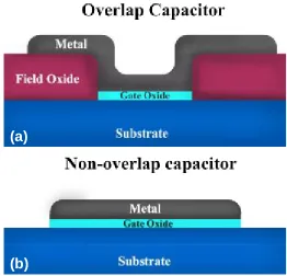
Figure 2.2a shows the cross sectional schematic of an overlapped MOSCAP. Slightly different from non-overlap capacitors (Fig. 2.2b), these overlap capacitors overlap the active area and spill onto the isolating field oxide. These devices are fabricated on the same chip as the non-overlap capacitors which lack the overlap of the isolation oxide. The advantage of overlap capacitors is that any edge effects that may come about due to etching or other processing steps are dampened. However, this leads to a small error in device area and hence in capacitance. This error is minimized by making the FOX sufficiently thick, so that the resulting overlap capacitance is small compared to the active area capacitance. This error, however, can in turn affect the data extraction and lead to slightly more error then would be found in a non-overlap capacitor. Unless explicitly stated, capacitor data comes from overlap capacitors.
2.2 Standard Characterization Techniques
performance. All measurements were done in a Cascade Model 11000 probe station. The station is equipped with a Temptronics TP0315B temperature controlled chuck, which allows measurement at elevated temperatures. Unless otherwise noted, all measurements were taken at room temperature in the absence of light.
2.3.1MOSCAP
As previously mentioned, there is a wealth of information that can be obtained from MOSCAPs, particularly from capacitance versus voltage (CV) measurements. All capacitance versus voltage measurements were made with the HP4284. Before any measurement session is started, an open circuit meter correction is done internally to compensate for parasitic capacitances in the signal path and measurement station. Once probed, the gate of the capacitor is stepped to a given DC bias, while a small signal AC sine wave is superimposed. The resultant AC current is read to determine the complex impedance. The impedance data is modeled inside the meter as a resistor and capacitor in parallel [6]. The resistor is typically modeled as a conductance with the equivalent 1/R value. The measured capacitance and conductance values are then read into a computer which is driving the meter and corrected according to the series resistance [7]. For all the data in this work, the series resistance and AC conductance was low enough to give very good agreement between the measured CV curve and the corrected CV curve. CV data are finally run though a NCSU curve fitting program [8] to extract electrical and physical parameters.
across the gate. To minimize charging effects at low bias, IV measurements are always started at zero bias and stepped towards either the positive or negative maximum. Leakage data are then converted to effective oxide field for comparison using equation 2.1
(
)
EOT V V
Eeff = g − FB (2.1)
2.3.2Interfacial Trap Measurements from Conductance
Interfacial oxide traps in MOSCAPs can affect the capacitance versus voltage behavior. Interfacial states can trap carriers and act as recombination sites affecting lifetime and mobility. The conductance measurement made during a CV measurement can be very sensitive to the interfacial trap density and the position of the traps within the Si bandgap [9]. In this measurement the MOSCAP is modeled as a passive circuit with the oxide capacitance (COX), in series with the parallel combination of the semiconductor capacitance (CS) and the
interface state capacitance (Cit) and conductance (Git = Rit-1) (fig 2.3a). This model is
simplified to a three device system (fig 2.3b) with
( )
[
2]
1 ln
2 it it
it
P qD
G
ωτ ωτ
ω = + (2.2)
and
(
)
21 it
it S
P
C C
C
ωτ
+ +
representing the equivalent parallel capacitance and conductance. Here Dit is the density of
interface states and τit is the interface trap time constant. From these equations a plot of GP/ω
against ω will give a maximum at
it τ
ω = 2 (2.4)
with a corresponding density of interface states
ω
q G
D P
it
5 . 2
= (2.5)
The use of eqs. 2.4 and 2.5 can yield a large amount of useful information about interface trap densities and characteristic time constants as a function of bias.
G
P
C
OX
C
P
C
OX
C
it
R
it
C
S
(a)
(b)
G
P
C
OX
C
P
C
OX
C
it
R
it
C
S
(a)
(b)
Figure 2.3: Circuit model for Dit measurement on MOS capacitors (a) and simplified
model (b). The conductance term has no dependence on CS and therefore is
2.3 Memory Device Characterization
A handful of non-standard MOSCAP measurement techniques which are specific to memory device characterization were used for the course of this work. For the most part, these techniques build off of the basic IV and CV measurements described in the previous session and involve timing, sequencing, or specially analyzing the standard measurements to obtain new views of data. However, since the state of a memory device is intrinsically dependant on what biases and stresses were previously applied, special care is needed to know what the initial (pre-measurement) state was and to minimize disturbing the device state by measuring it.
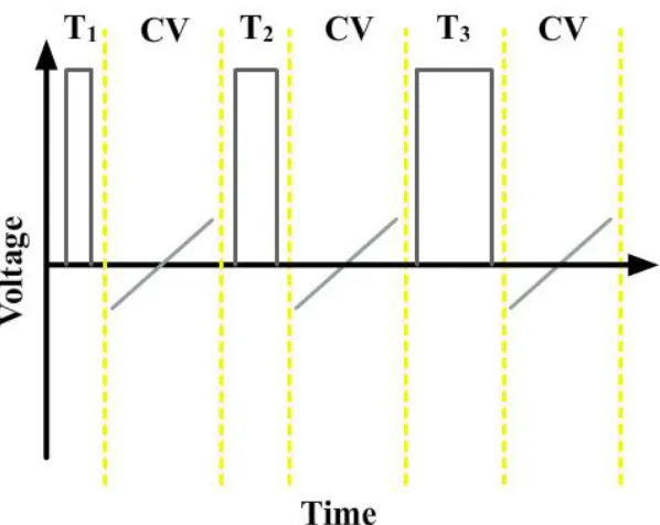
2.3.1Memory Window
Measuring the difference between the programmed and the erased state (the memory window) of a charge trapping device is one of the most basic memory measurements. The technique involves applying voltages at time periods that approach charge saturation in the charge trap layer, then measuring the change in VFB (capacitors). For capacitors, this is
achieved in one of two ways, the hysteresis method or the stress and sense method.
In the hysteresis method (fig 2.4a), the CV curve is measured in both the negative to positive direction, and the positive to negative direction. The range of each sweep starts at low enough bias to capture the entire CV curve, and then is progressively increased on subsequent sweeps. The data can then be processed as a normal CV curve, and the physical parameters extracted. The difference in VFB between the forward and reverse sweeps for a
hysteresis method are its relative ease in implementation and data processing. However the hysteresis method can be a lengthy measurement especially when high voltages are involved. There are also limits to the time resolution of each step due to the minimum length of time needed to determine the capacitance at each point.
The stress and sense method for determining the memory window of a device overcomes some of the shortcomings of the hysteresis method. In this method the initial state of the capacitor must be know, either by measuring or by forcing the device into a known state. Then a relatively high bias (stress) is placed on the gate of the MOS device for a predetermined amount of time, after which a CV measurement (sense) is made at the lowest voltage range possible to reduce the disturbance caused by the measurement process (fig. 2.4b). The VFB of the device can then be extracted and compared to the initial state to
determine the memory window. This method has the main advantage of precise control of the
(b)
(a) (b)
(a)
Figure 2.4: High frequency CV curves and applied biases for memory window
stress time and voltage and more closely mimics the actual operation of a memory device. However, the stress and sense method is more complicated to implement. Often it is necessary to have a rough idea of how the device will respond to the bias to be able to accurately set the range for the sense measurement.
Because of the simplicity of the hysteresis method and the fact that the information gained from it can be used to set the stress levels and estimate the sense range, it is the most common measurement performed. Unless otherwise stated, the hysteresis method was used to obtain memory windows and the stress and sense method was used only where precise timing was necessary or where minimizing disturbs in sense operations is critical.
2.3.2Program / Erase Time
The time required to write or erase a flash memory device is an important parameter to determine the performance of a memory device. Faster program erase times lead to faster data transfer rates when writing to a flash array. There is, however, a trade off in program erase times and memory window. Typically, smaller times imply less charge is being injected into the floating gate, less charge being trapped, and less of a shift in VFB. A smaller memory
window would then require longer sensing times during a read operation and longer times for transferring data off of a flash array.
Program / erase (P/E) measurements are made by programming with a high speed pulse generator and then reading the shift in VFB with a capacitance meter. Careful setup is needed
above. Voltage limits for a CV sweep are then determined to minimize P/E disturbs. Ideally the voltages required during a CV sweep to obtain a value of VFB for a given measurement
should be less then the voltage required to achieve that shift (fig 2.5), and more specifically the range of biases in a CV measurement should fall in a region which shows negligible VFB
shift. The minimum and maximum measurement voltage limits are determined for the initial, program, and erase CV measurements based on the VFB shift expected and the voltage range
which showed negligible VFB shift from memory window measurements by the hysteresis
method.
To determine the time dependence on program and erase VFB shifts separately, the
initial CV is first read. Then the device is stressed with a voltage pulse to either program or erase it. The voltage is selected based on hysteresis measurements and the pulse width is
logarithmically swept from lower to higher times. Immediately after stressing the capacitor, the capacitance is measured using the voltage limits expected to capture the expected shift while still minimizing inadvertent charging or discharging of the devices. The measurement biases are illustrated in figure 2.6 and intended to minimize disturbs to the charged state.
2.3.3Retention
The ability for flash memory to retain its charge is not trivial to determine. The ITRS requires next generation devices to have retention times >10 years [10]. But spending 10 years to measure a single device is simply not feasible, so the data must be determined in a reasonable time frame (hours to days) and extrapolated out to the 10 year mark with accuracy. This extrapolation is often made by heating the sample during the measurement to
speed the charge loss, and to increase and determine the effect of different charge loss mechanisms.
The basic retention measurement is performed by charging up a device, then periodically measuring VFB to determine how it varies over time. The charging time and
voltage is determined from the P/E time plot as described above. The initial state of the capacitor is read, or in some cases an initial state is forced by applying stress and then read. For retention measurements it is also critical to determine appropriate sense voltages for CV measurements so as to minimize or eliminate any charging or discharging caused by the sense operation during the measurement. This is achieved in the same manner as the P/E time measurements, with the one difference being that the sense time now must be broad enough to cover a changing flat band voltage over a long period of time and hence possibly a large
range. In practice this is a near trivial consideration, since in the case of both the program and erase measurements the ∆VFB tends to decay towards zero and hence the voltage limit which
needs to be extended typically falls in a lower field region then the other limit and would result in less disturbance. The applied bias as a function of time is illustrated in figure 2.7.
Although 10 year retention must be met, it’s impractical to measure a single device for anywhere near this time scale. Therefore other methods are used to extrapolate the 10 year mark. The simplest method is to simply measure retention for a moderate period (~105 s) and then fit a line to the data and extrapolate out to the 10 year mark. This method is simple and quick but also a gross approximation. More accurate methods involve measuring the sample under different forms of stress to accelerate the charge de-trap mechanisms. By varying the stress levels, more accurate 10 year retention can be determined after a few hours or days of measurement. Typical stressing methods include temperature [11] and electric field [12]. Accelerating charge de-traping mechanisms greatly reduces the measurement time, but care must be taken to identify dominant mechanisms as the different forms of de-trap acceleration don’t affect all mechanisms equally.
2.3.4P/E Cycling Reliability
in ∆VT [10]. In addition, the SILC degradation must be little enough to still maintain the 10
year retention requirements after 105 P/E cycles.
Measuring the memory window as a function of program and erase cycles is accomplished by extending the P/E time measurement out to thousands or hundreds of thousands of cycles. Again this is accomplished using a high speed pulse generator. After determining the write and erase voltages, and times from the P/E time measurements, a waveform, mimicking the chosen conditions, is applied continuously (Fig 2.8). The continuous waveform is interrupted at predetermined intervals and a CV curve is measured after both a write and an erase cycle of the waveform. From the CV data, a VFB value is
extracted and the difference between it and the initial VFB can be determined to quantify the
change in VFB, and the overall change in memory window.
2.4 Physical Characterization
Through the course of this work a handful of very useful analytical techniques have been used to gather more information about both nano-particles and the devices fabricated from them. Imaging and sizing particles has be accomplished for relatively larger sized nano-particles using secondary electron microscopy (SEM). For smaller nano-particles atomic force microscopy (AFM) has shown some merit, although the most accurate size measurements have come from transmission electron microscopy (TEM) images. Besides these imaging techniques, x-ray photoelectron spectroscopy (XPS) was used to investigate the chemical bonding energies and elemental composition of ALD films. The following section describes the advantages and shortcoming of all of these techniques.
2.4.1SEM
In SEM, a relatively low energy electron beam (5 kV to 20 kV) is focused and rastered across the sample surface. The incident electrons collide with the sample and in the collision, some energy is given to secondary electrons within the sample. This energy often is enough to eject secondary electrons from the sample which are collected in a detector. The amount of electrons collected is interpreted as contrast on a monitor and by syncing the beam raster with the monitor’s raster an image of the can be constructed [14].
and even sub nm, are easily accomplished. However, the relatively low energy of the beam and the collision with the sample create a characteristic tear drop shape area inside the sample in which the secondary electrons are excited. This effectively increases the minimum spot size and leads to a reduction in the sharpness of features at high magnification and hence additional error in determining the feature size. Additionally for closely spaced features the noise and secondary electrons from adjacent structures can lead to a near complete lack of resolution in SEM images. Because of these limitations the effectiveness of SEM as a tool for imaging nano-particles is limited to particle sizes and spacings roughly >15nm.
2.4.2TEM
TEM is a technique which greatly extends the resolution of electron microscopy compared to SEM. Similar to SEM, a beam of electrons is focused onto the sample, however in TEM imaging beam energies are much higher typically around 200 kV. Like a SEM, this electron beam can be rastered as in scanning TEM (STEM), but that is not always the case. The high energy electron beam incident on the surface travels though the sample and out the backside into an electron detector, typically a charge capture device (CCD). The spatial variations in the electron beam amplitude and phase at the detector can be reconstructed into an image of the specimen [14].