(www.dvpublication.com) Volume 4, Issue 2, 2019
1
OFFSET REDUCTION IN THE DOUBLE TAILED
LATCH-TYPE VOLTAGE SENSE AMPLIFIER
Abhinav V. Deshpande
Internal Full Time (IFT) Ph. D. Research Scholar, School of Electronics Engineering (SENSE), Vellore Institute of Technology (VIT), Vellore, Tamilnadu
Cite This Article: Abhinav V. Deshpande, “Offset Reduction in the Double Tailed
Latch-Type Voltage Sense Amplifier”, International Journal of Advanced Trends in Engineering and Technology, Volume 4, Issue 2, Page Number 1-5, 2019.
Abstract:
This research paper presents an improved double tailed latch type voltage sense amplifier by using a latch load in the first stage. A latch load at the first stage provides the second stage with a large input difference voltage. Thus, completely removes the offset voltage due to the mismatch in the transistor pairs in the second stage of the Sense Amplifier. The performance of the Sense Amplifier was simulated by using the LT Spice with a threshold mismatch of 10% in between the transistor pairs of the second stage, where it achieved the offset removal at 3 GHz clock rate with VDD = 1. 2 Volts in a 90 nm CMOS technology. Since the input transistors of the first stage are in parallel with the transistor pair of the latch, it does not affect the delay.
Key Words: Offset Reduction, Double Tailed Latch Type Voltage Sense Amplifier, Analog to Digital Converter (ADC), Differential Voltage
Introduction:
A comparator has a crucial influence on the performance of the Analog to Digital Converter (ADC). The ADC performance is affected by the comparator offset, speed and the power consumption. The high speed and the high-resolution ADC architectures require accurate and high-speed comparators. A high-performance comparator needs to amplify a small input voltage to a large enough level, which is detectable by digital logic circuits within a very short time. Therefore, a high gain and high bandwidth is required in the accurate and the high-speed comparators. The technology scaling of the MOS transistors enables the high speed and the low power operation but the offset voltage of the comparator is increased due to the transistor mismatch. In the conventional designs, pre-amplifiers are used to reduce the offset voltage [1]. However, these techniques require a high voltage gain in order to reduce the offset voltage and loosing the effectiveness with the reduction of the drain resistance due to the technology scaling. Moreover, a large power consumption of the amplifier is inevitable for realizing a wide bandwidth amplifier. On the other hand, a dynamic comparator which has the offset compensation function was proposed by [2].
International Journal of Advanced Trends in Engineering and Technology (IJATET) Impact Factor: 5.965, ISSN (Online): 2456 - 4664 (www.dvpublication.com) Volume 4, Issue 2, 2019
2
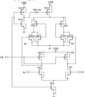
In this method, the same input signal of each comparator as the reference voltage is given in the flash type ADC, and the load capacitances of the output node of each comparator are controlled digitally so that the output of the comparator may reach the ideal value. However, the calibration time greatly increases if the resolution of the ADC is increased. Moreover, the speed of the comparator is slowed down due to the increase of the added capacitances. Additionally, the considerably large size circuits in order to control the calibration are necessary for each comparator. Therefore, this topology is improper for the design of a high-resolution flash type ADC’s. A Double Tailed Latch Type Voltage Sense Amplifier which is shown in Figure 1 is a comparator with a high speed, low offset, low power consumption [3]. However, this design reduces the effect of the offset voltage due to the mismatch in the second stage (M6 and M7, M8 and M9, M10 and M11), it cannot remove it completely because of the lower differential voltage at the second stage as shown in Figure 2. In this research paper, a double tailed latch type Sense amplifier with the latched load is proposed. In these proposed Sense Amplifiers which are as shown in Figure 3 and Figure 4, a latch is used as a load in the first stage for a large differential voltage for the second stage input to remove the offset completely. As shown in Figure 6 and Figure 7, the differential voltage is wide enough in order to overcome a wide range offset voltage in the input of the second stage.
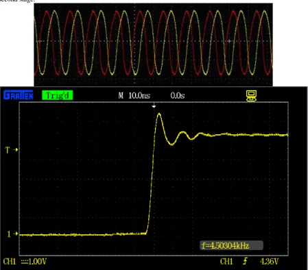
Figure 2: Waveform of Double Tail Latch Type Voltage Sense Amplifier (a) Differential Voltage Di+ and Di-, (b) Output Out 1 and Out 2
Circuit Design:
(www.dvpublication.com) Volume 4, Issue 2, 2019
3
Figure 3: Double Tail Latch Type Voltage Sense Amplifier with a Latched Load (Cascade Connection)
Figure 4: Double Tail Latch Type Voltage Sense Amplifier with a Latched Load (Parallel Connection)
3. Operation:
Both of these structures operate in a similar way. During the reset phase (when CLK = 0 Volts and CLKB = VDD), the transistors M4 and M5 pre-charge the Di nodes to VDD, which causes M10 and M11 to discharge the output nodes to the ground. After the reset phase, in the evaluation phase (when CLK = VDD and CLKB = 0 Volts), the tail transistor M1 and M12 turns ON and the latch of the first stage starts regenerating depending on the input differential voltage (Vin 1 – Vin 2), thereby producing a large difference voltage. This difference voltage is sensed at the second stage input and the second stage latch regenerates the output voltage OUT1 and OUT2 which is as shown in Figure 6 and Figure 7.
International Journal of Advanced Trends in Engineering and Technology (IJATET) Impact Factor: 5.965, ISSN (Online): 2456 - 4664 (www.dvpublication.com) Volume 4, Issue 2, 2019
4
(www.dvpublication.com) Volume 4, Issue 2, 2019
5
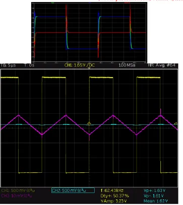
Figure 7: Waveforms of a Double Tail Latch Type Voltage Sense Amplifier with a Parallel Connection (a) Differential Voltage Di+ and Di- (b) Output Voltage Out 1 and Out 2
Simulation Results:
In order to compare both these Sense Amplifiers (SA’s), both the circuits are simulated in the LT Spice Simulator with the same transistor dimensions (here it is assumed that the first stage of both the DS’s are completely matched). The operating conditions are VDD = 1.2 Volts and FCLK = 3 GHz and the input has a common voltage VCM = 0.6 Volts. The proposed Sense Amplifier shows a zero offset for any of the transistor pair mismatch in the second stage. The offset voltage for the mismatch in the transistor pairs of the second stage is shown in Table 1. For the mismatch of the transistor pairs M1 and M2 all of the three Sense Amplifiers have the same offset voltage.
Table 1: Offset Voltage for the Mismatch in the transistor pairs of the second stage
SA’s Offset in mV Due to Mismatch in the Transistor Pair
M6 & M7 M8 & M9 M10 & M11
Conventional SA 4 2 3
SA with a Cascade Connected Latch Load 0 0 0 SA with a Parallel Connected Latch Load 0 0 0
Conclusion:
A Low power and low offset sense amplifier by using a latched load is being proposed in this research paper. The latch load effectively removes the offset voltage in the second stage. Thus, the overall offset voltage (when the offset in the first stage is considered) of the sense amplifier and can be reduced by using the latched load. However, for the sense amplifier with a cascade connected latch the delay is increased where as for the sense amplifier with a parallel connected latch the delay remains the same but it needs an accurate timing of the CLKB. The results which are obtained from the process of the simulation confirm the advantages of the proposed sense amplifiers.
References:
1. B. Razavi, “Principle of Data Conversion System Design”, IEEE Press
2. G. Van der Plas, S. Decoutere and S. Donnay, “A 0.19Pj/Conversion Step 2.5 mW 1.25GS/sec 4-bit ADC in 90 nm Digital CMOS Process”, ISSCC Dig. Of Technical Papers, pp. 566-567, February 2006. 3. Daniel Schinkel et al, “A Double Tail Latch Type Voltage Sense Amplifier with a 18 ps Set up plus
Hold Time”, ISSCC Dig. Of Technical Papers, pp. 314-315, February 2007.