Design and Implementation of Convolutional
Encoder and Viterbi Decoder
1
Siddharth Tata,
2Suguri Charan Kumar,
3Varampati Reddy Kumar
1,2,3Dept. of ECE, GITAM University, Hyderabad, India
Abstract
The main aim of this project is FPGA implementation of the convolutional encoder and Viterbi decoder which will allow the receiver to detect and correct any errors without the need for retransmission. The Convolutional Encoder and the maximum likelihood Viterbi decoder solve the problem of the transmission of data in an erroneous channel. This project is aimed at designing and implementing the encoder and decoder on an FPGA so that the receiver can detect and correct any errors without the need for retransmission.
Keywords
ATLYS SPARTAN 6 FPGA Development BoardChip Scope Pro Analyzer.
I. Introduction
A. Problem Statement
Besides the attenuation of the signal in the long-distance transmission, every communication channel is exposed to different kinds of noise sources such as the Anti-White Gaussian noise (AWGN) which fluctuates the voltage around the threshold. The real problem arises when you discover that the received data has been corrupted and you have to retransmit the whole data again. However, retransmission is not efficient as it wastes a lot of time and this is not acceptable in applications especially with the advanced communication systems which have a very high data rate. Therefore, there is a need to efficiently transmit data without the need for retransmission.
B. Contributions
The contributions of this work are as follows:
Design a convolution encoder of rate = ½ and constraint length = 3. Design a Viterbi Decoder and implement it on an FPGA so that there is no need for retransmission.
II. System Design
A. Architecture
Fig. 1: Block Diagram of a Communication System
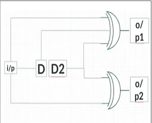
B. Design of Convolutional Encoder
A convolutional encoder is an encoder in which the output depends not only on the current input information, but also on previous inputs or outputs, either on a block-by-block or a bit-by-bit basis. There are applications in which the message bits come in serially rather than in large blocks, in which case the use of a buffer may be undesirable. In such situations, the use of convolutional coding may be the preferred method. A convolutional coder generates redundant bits by using modulo-2 convolutions-hence the name of the coder. The convolutional encoder can be represented as a Finite State Machine (FSM) with given number of shift register stages, e.g., if there are a K-stage shift registers (usually D flip flops) with rate of encoder input bits to its output, is 1/n and an L bit length message; the coded output sequence will have length of n (L+K) bits. Also, the code rate of the convolutional code is therefore given by:
R = L / n (L + K) bits/symbol
Fig. 2: Convolutional Encoder
The most common convolutional encoders have the following parameters:
1. K=2 & rate=1/2 2. K=2 & rate=2/3
The first block of the three delay blocks (D-flip flops) in the below figure represents the input and both the other two blocks are D-flip flops operating as a shift register to save previous states. Each state leads to two possible states depending on the new arrival input.
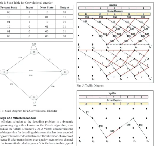
Table 1: State Table for Convolutional encoder
Present State Input Next State Output
00 1 10 10
10 0 01 11
01 1 10 01
10 0 01 11
01 0 00 11
00 0 00 00
Fig. 3: State Diagram for a Convolutional Encoder
Design of a Viterbi Decoder:
An efficient solution to the decoding problem is a dynamic programming algorithm known as the Viterbi algorithm, also known as the Viterbi Decoder (VD). A Viterbi decoder uses the Viterbi algorithm for decoding a bitstream that has been encoded using convolutional code or trellis code.The likelihood of a received sequence Ŕ after transmission over a noisy memoryless channel for the transmitted coded sequence Ṽ is the basis in this type of decoding. Viterbi Decoder is a maximum likelihood decoder, in the sense that it finds the closest coded sequence ṽ to the received sequence ŕ by processing the sequences on a bit-by-bit (branches of the trellis) basis. In other words, instead of keeping a score of each possible coded sequence, it tracks the states of the trellis.
Fig. 4: Block Diagram of Viterbi Decoder
Fig. 5: Trellis Diagram
Fig. 6: Survivor Path
III. Implementation
A. Hardware and Software Tools
The hardware tool used for this project is ATLYS SPARTAN 6 FPGA DEVELOPMENT BOARD. A software tool used for this project is Xilinx ISE Design Suite 14.5.
B. ATLYS SPARTAN 6 FPGA Development Board
Table 2: Noof components used in Convolutional encoder and Viterbi Decoder Combined System.
Component Number of Components used
Slice Registers 206
Slice LUTs 325
LUT Flip Flop Pairs 348
IOBs 15
BUFG/BUFCTRL/
BUFHCEs 1
C. Design Entry Using Xilinx ISE Design Suite
In the design entry process, the behavior of the circuit is written in hardware description language like VERILOG. Simulation and synthesis are the two main kinds of tools, which operate on the VERILOG language.
D. ChipScope Pro Analyzer
Before generating the bitstream file we have to add chip scope pro cores to the topmost module and then generate the bitstream file. Chip Scope Pro allows you to embed the following cores within your design, which assist with on-chip debugging: integrated logic analyzer (ILA), integrated bus analyzer (IBA), and virtual input/ output (VIO) low-profile software cores. For debugging purpose cores that are to be added can be an integrated controller core (ICON) or ILA core or IBA core and virtual input/output core.
The Convolutional Encoder consists of the units ‘rs’, ‘sd’, ‘top shifter’ and ‘fde’.The ‘rs’ unit takes the 6-bit input and transfers it bit by bit to the ‘sd’ unit. The ‘sd’ unit then gives the 2-bit output corresponding to the input and sends these 2 bits to the ‘opshifter’ unit which inturn acts like a shift register shifting two bits to the right at a time. The ‘fde’ unit gives the encoded output through the wire ‘op’ once all the encoded bots have been received from the ‘opshifter’ unit.
Fig. 7: RTL Schematic of Convolutional Encoder
The Viterbi Decoder consists of the units ‘bmu’ and ‘acs’. The ‘bmu’ unit is the branch metric unit which calculates the branch metric for all the branches in the trellis diagram corresponding to the Viterbi decoder. The ‘acs’ unit is the add, compare and select a unit that selects the branch with the smallest possible metric reaching every node in the Trellis diagram. The ‘acs’ unit also consists of the traceback unit that calculates the survivor path and the corresponding decoded output.
Fig. 8: RTL Schematic of Viterbi Decoder
IV. Results
The Simulation result of the encoder has a rate that is equal to 1⁄2 which is for one bit of input there are two bits of output. The input is given to the encoder through the wire ‘ip’ and the output is obtained through the wire ‘op’. The input given in the above case is 6-bit binary value ‘100100’ and the output so obtained is 12-bit binary value ‘101111101111’.
Fig. 9: Simulation Result of Convolutional Encoder
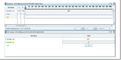
This ChipScope Pro result consists of the waveform generated by the ILA and the output of the VIO console. The input is given through the VIO console signal ‘encoder in’ and the output is obtained through the signal ‘encoder out’. The input given in the above case is the hexadecimal value ‘24’ which is equivalent to the binary value ‘100100’ and the output obtained is the hexadecimal value ‘BEF’ which is equivalent to the binary value ‘101111101111’.The same output can also be seen as the ‘encoder out’ signal in the ILA waveform.
Fig. 10: Chip Scope Pro of Convolutional Encoder
the wire ‘do1’. The input given in the above case is 12-bit binary value ‘101111101111’ and the output so obtained is 6-bit binary value ‘100100’.
Fig. 11: Simulation Result of Viterbi Decoder
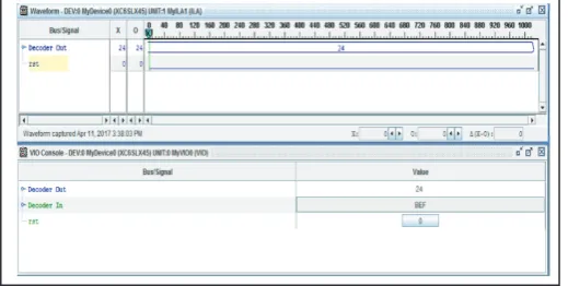
This ChipScopePro result consists of the waveform generated by the ILA and the output of the VIO console. The input is given through the VIO console signal ‘Decoder In’ and the output is obtained through the signal ‘Decoder Out’. The input given in the above case is the hexadecimal value ‘BEF’ which is equivalent to the binary value ‘101111101111’ and the output obtained is the hexadecimal value ‘24’ which is equivalent to the binary value ‘100100’.The same output can also be seen as the ‘Decoder Out’ signal in the ILA waveform.
Fig. 12: Chip Scope Pro of Viterbi Decoder
V. Conclusions
The aim of this project is the design and implementation of a convolutional encoder and a Viterbi decoder that can encode a bitstream of digital information while transmission and later decode it while reception. The encoder was designed with constraint length 3 and rate 1/2. For decoding, the Viterbi Algorithm is widely used as it eliminates the potential noise in a data stream. The characteristics of the Viterbi decoder are its effectiveness in noise elimination, the speed of decoding and cost (hardware utilization). For implementation, FPGAs are the new solutions used by many engineers to implement computationally intensive algorithms. FPGAs offer the best of all the worlds, the flexibility of a programmable solution, the performance of a custom solution, and lowering overall cost. So, keeping in view of the advantages of using FPGAs as compared to other customized devices, the FPGAs can further be utilized for designing & implementation of a generic Viterbi decoder. The genericity of the design facilitates not only the rapid prototyping of Viterbi decoders with different specifications but moreover, it explores the performance of different implementations in order to obtain the most suitable solution for a particular communication system. Some of the generic parameters such as basic decoder specifications, metric size, trellis window length, the number of surviving paths and pipeline depth can be changed for achieving new specifications and
these new specifications can be realized by only re-synthesizing the code.
VI. Future Scope
This project objective is to encode and decode data correctly, so any improvement made will be a performance matter. Each encoder and decoder parameter can be improved by modifying the Verilog HDL code and this can be done only if there are enough resources for this modification. There are many recommended processes that can be added in the future as the next step of system development: Increasing the constraint length and developing new generation matrices; this will increase bit memory time intervals leading to less BER and more ability to correct burst error. The register exchange survivor path method has a high-power dissipation and needs large memory space while the traceback method has more latency. The design of hybrid tracing system of traceback and trace forward (register exchange) that has the advantages of both will effectively increase the performance. Another area of challenge is that of developing codes with larger number of errors. BCH and some other designed codes turn out to be inefficient for increasing number of errors. Small codes with desired error correction capabilities can be easily developed; developing large codes presents a real practical problem. A practical way to obtain large codes is to obtain them by suitable composition of those of shorter lengths. Our goal is to build codes with larger size or longer length from code of smaller size or shorter length.
References
[1] Arun, C, et.al,"Design and VLSI Implementation of a Low Probability of Error Viterbi Decoder”, IEEE International Conference, Vol. 3, Issue 1, pp. 418-423, 2008.
[2] HEMA.S, Suresh Babu.V, Ramesh P.,“FPGA Implementation of Viterbi Decoder”, Proceedings of the 6th WSEAS Int. Conf. on Electronics, Hardware, Wireless and Optical Communications, Corfu Island, Greece, February 16-19, 2007.
[3] Prof. Siddeeq Y. Ameen, Mohammed H. Al-Jammas, Ahmed S. Alenezi,"FPGA Implementation of Modified Architecture for Adaptive Viterbi Decoder", 2011.
[4] Saleem, S. et.al,"Design and Tradeoff Analysis of an Area Efficient Viterbi Decoder”, IEEE international conference, Vol. 1, Issue 1, pp. 1-5, 2007.
[5] Yang min,"Design optimization of FPGA based Viterbi decoder”, IEEE international conference, Vol. 1, Issue 1, pp. 4129-4131, 2011.
[6] ArkadiyMorgenshtein, Fish, I. A. Wagner,“Gate-diffusion input (GDI) – A novel power-efficient method for digital circuits: A detailed methodology”, In Proc. 14th IEEE International conference 2001.
[7] Spartan-6 FPGA Configurable Logic Block User Guide Xilinx documentation.
Mr. Tata Siddharth has pursued his undergraduate studies in Electronics and Communications Engineering at GITAM University, Hyderabad in the year 2017. He has been working in Cognizant Solutions on UI Development. His penchant towards the Machine Learning and Computer Science course has helped him in deep research and execution of several projects successfully. He had researched and built a Weather Prediction Model, which has improved the accuracy of predicting the weather changes by 15 %. He has built an efficient model that predicts a student’s performance in a course, using Logistic regression and Feature Engineering. He is currently working on the development of a complete website with user interactions with a dynamic, suggestive response by the developer contingent of the company to its client.
Mr. Suguri Charan Kumar has pursued his undergraduate in Electronics and Communications Engineering at GITAM University, Hyderabad. He is currently working in Cognizant Technology Solutions as a Programmer Analyst. With a predilection towards the Data analysis and Data Management, he is relentlessly researching in the field of Data Science. He had successfully implemented a Low Leakage 32 Bit Parallel Prefix Adder during his Sophomore years. He is currently working on the development and enhancement of Data Management models in his company.