[Gomez* 5(11): November, 2018] ISSN 2349-4506
Impact Factor: 3.799
G
lobal
J
ournal of
E
ngineering
S
cience and
R
esearch
M
anagement
A METHODOLOGICAL APPROACH FOR SPIRAL INDUCTOR DESIGN AND
OPTIMIZATION
Frederick Ray I. Gomez
*
New Product Introduction Department, Back-End Manufacturing & Technology, STMicroelectronics,
Inc. 9 Mountain Drive, Light Industry & Science Park II, Brgy. La Mesa, Calamba City, Laguna,
Philippines 4027
DOI: 10.5281/zenodo.1745384
KEYWORDS
:
Inductor, Q-factor, inductance, inductor design.ABSTRACT
The technical paper presents a methodological and fundamental approach for design and optimization of a spiral inductor using tools namely Analysis and Simulation of Spiral Inductors and Transformers for ICs (ASITIC) and Integrated Spiral Inductor Calculator (SpiralCalc). Both software tools are available for research and academic purposes. Inductors are key components esp. for impedance matching and are designed such that they would exhibit a high Q-factor (quality-factor) for the specific inductance and frequency range of operation. A sample value of 5.3 nH is set for this paper for the spiral inductor design using the tools. For optimum Q-factor, an octagonal geometry for spiral inductor is used for ASITIC design, to have a close comparison to that of the SpiralCalc. Design methodologies for the optimization of the spiral inductor parameters such as the inductance and the Q-factor are discussed. Results comparison between the two tools is also presented. Design tradeoffs between inductor parameters are inevitable, and these parameters affect the performance of the inductor especially at higher frequencies. With this, it is crucial that inductors be designed carefully for their effective frequency range of operation and specific requirements of the intended application.
INTRODUCTION
Monolithic implementation of on-chip passive components of RFIC (radio frequency integrated circuit) has become highly preferred by designers and researchers as it provides high level of integration with cost, area, and power savings [1]. These passive components such as resistors, inductors, and capacitors, should be carefully designed and if possible have characteristics and performance close to ideal to satisfy the high quality and high performance requirements. Inductor in particular, is a key component for impedance matching and for RF applications. It is designed such that it would exhibit a high Q-factor or simply Q (Quality-factor) for the specific inductance value and frequency range of operation [2]. Q-factor, on the other hand, is used as basis to compare and rate the performance of the inductor. Design tradeoffs between inductor parameters are inevitable, so it is crucial that inductors be designed carefully for the specific requirements of the intended application.
DESİGN METHODOLOGY
For the design and optimization of a spiral inductor or more specifically the Q-factor of the spiral inductor, succeeding paragraphs for design rules and guidelines could be very useful.
[Gomez* 5(11): November, 2018] ISSN 2349-4506
Impact Factor: 3.799
G
lobal
J
ournal of
E
ngineering
S
cience and
R
esearch
M
anagement
Figure 1. Simplified layout of microstrip spiral inductor.
Increasing the conductor/strip/metal width (W) would make the Q-factor more sensitive to changes in operating frequency. Optimum values of metal width range between 10-15µm for most inductor designs fabricated commercially [3].
As the number of turns (N) of the spiral inductor increases, the outer dimension of the spiral (L) shrinks as well as the spacing between opposite sides of the spiral. This causes a drop in inductance and thus dropping the Q-factor because of negative mutual coupling.Q-Q-factor of the spiral inductor is most sensitive to the thickness and resistivity of the metal layer used in fabrication [3]. An increase in the conductor thickness causes the inductance to increase. Q-factor could therefore be optimized by increasing the conductor thickness. But as frequency increases, energy is dissipated by the finite resistivity of the metallization as well as in the conductive substrate. Q-factor then decreases due to the increasing dissipation of energy at higher frequencies. Typical metal thickness ranges from 1-3µm.
The oxide layer isolates the metal conductors from the silicon substrate. A thicker oxide layer reduces the shunt parasitics and dissipation, which improves the inductor self-resonant frequency. Ideally, this results to a better Q-factor.
Maintaining sufficient space between the inductor and its surroundings keeps unwanted parasitic effects from disturbing the inductor’s electrical characteristics [3]. A spacing of at least five line widths (5W) is recommended. For the design of the spiral inductor using freeware tools, usually the first three guidelines are the only ones available for the designer or researcher to vary or characterize. Tools like the Analysis and Simulation of Spiral Inductors and Transformers for ICs (ASITIC) [4] [5] and Integrated Spiral Inductor Calculator (SpiralCalc) [6] [7] [8], could be used to apply these design rules for the design and optimization of a spiral inductor. Both software tools are available for research, academic, and non-commercial purposes. In ASITIC, a technology file or tekfile is essential for the tool to run. Tekfile contains process specific parameters such as metal layer thicknesses and the sheet resistance of the various metal layers [3].
ASITIC and SpiralCalc were eventually used to design and optimize a spiral inductor. A sample value of 5.3nH is set for the inductor design and for comparison using the two tools. In ASITIC, a tekfile worstepi.tek is necessary.
Spiral Inductor Design using SpiralCalc
[Gomez* 5(11): November, 2018] ISSN 2349-4506
Impact Factor: 3.799
G
lobal
J
ournal of
E
ngineering
S
cience and
R
esearch
M
anagement
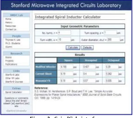
To acquire the needed inductance of 5.3nH, trial and error could be used with the turn spacing (S) and turn width (W) at optimal values which are 1µm and 10µm, respectively, as shown in Fig. 2.
Figure 2. SpiralCalc interface.
The modified Wheeler expression gives very good accuracy. This expression is obtained by modifying an expression that Wheeler obtained for discrete inductors [6] [8]. The current sheet expression is intuitive and is derived from electromagnetic principles by approximating the sides of the spiral by current sheets with uniform current distribution [7]. Lastly, the monomial fit expression is derived by data-fitting techniques. It is very well suited for optimization of circuits using geometric programming although it lacks intuitive derivation of the other two approximations [6] [7].
The input geometric parameters values in the SpiralCalc as shown in Fig. 2 that resulted to the desired inductance value could be used also to design the spiral inductor using the next tool which is ASITIC.
Spiral Inductor Design using ASITIC
This tool is more complex and challenging to use than the SpiralCalc. It uses commands to create or design the inductor and analyze its characteristics and behavior as the frequency varies.
Commands like ‘square’ and ‘spiral’ are used to create a square spiral and a polygon spiral, respectively. ‘Spiral’ command is often used because of its capability to create n-sided polygon spiral. It’s pretty straight forward to design using these commands. Input geometric parameter values must be provided and then it would create the layout of the spiral inductor. The values taken from the design of the inductor using SpiralCalc could be used as basis or for comparison for the design using ASITIC.
[Gomez* 5(11): November, 2018] ISSN 2349-4506
Impact Factor: 3.799
G
lobal
J
ournal of
E
ngineering
S
cience and
R
esearch
M
anagement
Figure 3. ASITIC interface, with command ‘optpoly’.
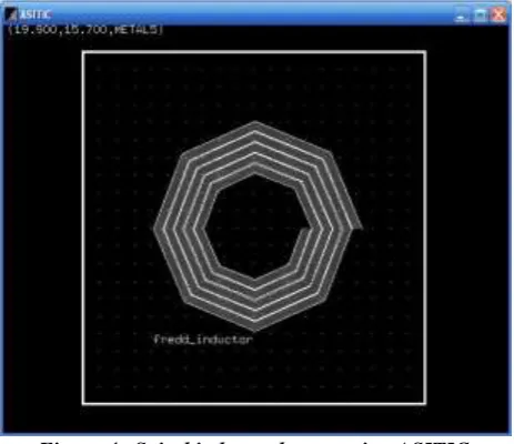
After the simulation using the ‘optpoly’ command and if it simulates successfully, a layout is produced as shown in Fig. 4. The layout could be moved in the cell view by using the command ‘move’ or ‘moveto’.
Figure 4. Spiral inductor layout using ASITIC.
To compute for the inductance, Q-factor, resonant frequency, S-parameters and Y-parameters of the spiral inductor over a frequency range, ‘2portx’ command is used. Each parameter could be modified by using the command ‘set’. Setting the mode of the analysis into “fast” would hasten the simulations. Setting it “slow” uses the Electromagnetic (EM) Analysis and it would take more time to run and finish the simulations. In this paper, “fast” mode is used.
RESULTS AND ANALYSİS
[Gomez* 5(11): November, 2018] ISSN 2349-4506
Impact Factor: 3.799
G
lobal
J
ournal of
E
ngineering
S
cience and
R
esearch
M
anagement
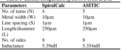
already shown in Fig. 2 given the input geometric parameters. Table 1 shows the comparison of the data and results of the two tools at DC.
Table 1 Results comparison of the two tools at DC. Parameters SpiralCalc ASITIC
No. of turns (N) 4 5 Metal width (W) 10µm 10µm Line spacing (S) 1µm 1µm Length/diameter
(L)
250µm 250µm No. of sides 8 8 Inductance 5.39nH 5.354nH
The data and results for the two tools are somehow comparable to each other. But this only applies at zero frequency or at DC. Table 2 tabulates the S-parameters of the spiral inductor from frequency 0-10GHz. These parameters are essential for the analysis of the behavior and characteristics of the spiral inductor.
The resonant frequency of the spiral inductor is where the Q-factor first reached zero (except for DC). It could be obtained by examining the results of the simulation in the ASITIC. Table IV shows the data for the inductance and Q-factor of the spiral inductor. ASITIC uses more complex formula to obtain the inductance and Q-factor versus frequency of the spiral inductor. But for this paper, the following formulae shown in Eq. (1) and Eq. (2) are used to obtain and approximate the inductance (L) and the Q-factor of the spiral inductor:
𝐿 =
𝑖𝑚𝑎𝑔(𝑍11)2𝜋𝑓
Eq. (1)
𝑄 =
𝑖𝑚𝑎𝑔(𝑍11)𝑟𝑒𝑎𝑙(𝑍11)
Eq. (2)
Table 2 Inductance and Q-factor.
[Gomez* 5(11): November, 2018] ISSN 2349-4506
Impact Factor: 3.799
G
lobal
J
ournal of
E
ngineering
S
cience and
R
esearch
M
anagement
5500 6000 7000 8000 9000 10000
532.346 94.166 18.879 8.707 6.149 5.814
-1017.228 -495.627 -228.976 -141.034 -92.782
-57.861
-29.43580 -13.14690 -5.20610 -2.80577 -1.64075 -0.92089
-1.91084 -5.26331 -12.12860 -16.19831 -15.08824 -9.95262
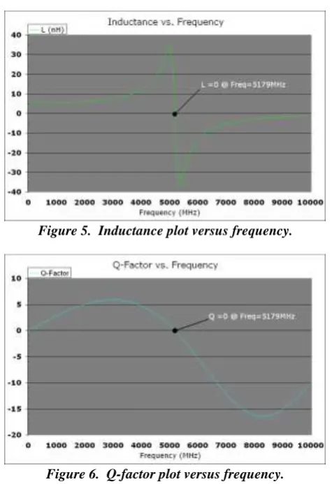
From the data in Table 2, the resonant frequency happened to be close at 5179MHz or 5.179GHz. In this frequency, the Q-factor is almost zero. It is also observed that the inductance L and the Q-factor became negative at frequencies above the resonant frequency. This is because the spiral inductor tends to act as a capacitor at frequencies above resonance. To have a better view of the behavior of the inductor, Fig. 5 and 6 shows the plots of the inductance L and Q-factor versus the frequency, respectively.
Figure 5. Inductance plot versus frequency.
Figure 6. Q-factor plot versus frequency.
CONCLUSİON
[Gomez* 5(11): November, 2018] ISSN 2349-4506
Impact Factor: 3.799
G
lobal
J
ournal of
E
ngineering
S
cience and
R
esearch
M
anagement
applicable only for ideal inductor. In addition, SpiralCalc used three different approximations for computing inductances but were valid only at DC and for limited design purposes. ASITIC revealed greater accuracy and could also be used for 3D Electromagnetic Analysis as well as 2D planar simplifications.
Complex tradeoffs among technology specifications and design parameters exist and should be carefully handled when designing an inductor, to optimize the quality and its performance. It is worth noting that inductors do not always behave as inductors as they may shift to capacitor operation at frequencies above resonance. Thus, it is crucial that inductors be designed for their effective frequency range of operation, satisfying the requirements of the end-product application.
ACKNOWLEDGMENTS
The author would like to extend the appreciation to Prof. Maria Theresa De Leon, Ph.D. of Microelectronics and Microprocessors Laboratory at University of the Philippines for the technical support during the course of the study, and to the STMicroelectronics Calamba NPI Team and the Management Team.
REFERENCES
1. Bowick, C., Ajluni, C., and Blyler, J. 2007. RF Circuit Design, 2nd ed. Newton, MA, USA: Newnes. 2. Gray, P. R., and Meyer, R. G. 1995. “Future Directions in Silicon ICs for RF Personal Communications.”
in Proc. IEEE Custom Integrated Circuits Conference, 83-9.
3. Long, J. R., and Copeland, M. A. 1997. “The Modeling, Characterization, and Design of Monolithic Inductors for Silicon RF IC’s.” IEEE Journal of Solid-State Circuits 32 (3): 357-69.
4. Niknejad, A. M., and Meyer, R. G. 2000. “ASITIC for Windows NT/2000.” Research in RFIC Design,
http://rfic.eecs.berkeley.edu/~niknejad/Asitic/grackle/cygwin_info.html.
5. Niknejad, A. M., and Meyer, R. G. 1997. “Analysis and Optimization of Monolithic Inductors and Transformers for RF ICs.” in Proc. IEEE Custom Integrated Circuits Conference: 375-78
6. Stanford Microwave Integrated Circuits Laboratory. Integrated Spiral Inductor Calculator. http://www-smirc. standford.edu/spiralCalc.html.
7. Mohan, S. S., del Mar Hershenson, M., Boyd, S. P., and Lee, T. H. 1999. “Simple Accurate Expressions for Planar Spiral Inductances.” IEEE Journal of Solid-State Circuits 34 (10): 1419-24.