© 2016, IRJET | Impact Factor value: 4.45 | ISO 9001:2008 Certified Journal
| Page 1336
RECTANGULAR MICROSTRIP ANTENNA LOADED WITH TUNNEL DIODE
Md Arif Ansari
1Prof. Ashok Kumar
2Praveen Kumar Mishra
31M.Tech, Electronics Dept. Kamla Nehru Institute of Technology Sultanpur (U.P.) India 228118
2 Professor, Electronics Dept.Kamla Nehru Institute of Technology Sultanpur (U.P.) India 228118
3
M.Tech, Electronics Dept. Kamla Nehru Institute of Technology Sultanpur (U.P.) India 228118
Abstract-A resonant frequency agile microstrip antenna with tunnel diode is proposed, in this the operating frequency is controlled by the bias voltage of the tunnel diode. The operating range of the described antenna is 55.92 MHz (6.67%), which is much better than the rectangular microstrip antenna.
Key words: rectangular microstrip antenna, tunnel diode,
bias voltage.
I. Introduction
Theoretically all the conducting element radiate electromagnetic wave but they are not efficient radiator that’s why we use some specifics size and shape. Microstrip patch antenna have many attracted feature like easy to manufacture, small in size, light in weight, and low cost. Microstrip patch antenna is most versatile antenna in today’s technology but their low gain and narrow bandwidth make these for limited use [1]. There are various technology for improving the gain and bandwidth (B.W.) of microstrip antenna [2]. One of them is use of active devices loaded microstrip. As in the case of multichannel application, small B.W. is required at a larger frequency range. In such applications instead of using a wide band antenna, a narrow band tunable antenna can be used [3, 4].
In the present paper work the study of different parameters of the symmetrically loaded, bias tunnel diode with rectangular microstrip antenna by using circuit model. The tuning frequency of the antenna is depends on the equivalent inductance ‘L’ and equivalent capacitance ‘C’. The equivalent capacitance can be changed by changing the junction capacitance ‘CD’ of the tunnel diode, which is
varies according to bias voltage applied to tunnel diode, which affect the overall tuning frequency [7, 8, 10].
II.Theoretical
consideration
and
antenna
equivalent circuit
2.1 circuit model of rectangular microstrip antenna
A rectangular microstrip antenna can be seen as a parallel combination of capacitance C InductanceL and resistance R, and the value of the above parameter is given by the modal expansion cavity model [2].
𝐶 =𝜀0𝜀𝑒 𝑤𝑙
2 𝑐𝑜𝑠
2 𝜋𝑦0
𝑙
𝐿 = 1
𝜔2𝐶
𝑅 = 𝑄𝑟 𝜔𝐶
And Qris given by
𝑄𝑟 =
𝑐 𝜀𝑒
4𝑓
Where ω=2ᴨfr, fr is designed frequency, c is the speed of
the light and εeis effective permittivity which is given by
𝜀𝑒 =
𝜀𝑟 + 1
2 +
𝜀𝑟− 1
2 1 +
10 𝑤
−1 2
Where εrand his the relative permittivity and the thickness
of the substrate material respectively, land W are length and width of the rectangular microstrip patch respectively.
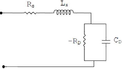
In tunnel diode equivalent circuit the inductance Ls resistance Rs are in series, and capacitance of the junction CD and negative resistance (-RD) are in parallel as shown below.
© 2016, IRJET | Impact Factor value: 4.45 | ISO 9001:2008 Certified Journal
| Page 1337
𝐶𝐷=𝐴𝑞𝜀 2 𝑉𝑖− 𝑉𝑏
𝑁𝐴𝑁𝐷
𝑁𝐴+ 𝑁𝐷
[image:2.612.39.249.208.327.2]Where, A is area of the junction, q is the electron charge, ε is the dielectric constant, (NA, ND) are concentration of the acceptor atom and concentration of the donor atom, Vi barrier potential and Vb is applied bias voltage.
Figure 1: equivalent circuit of the tunnel diode.
[image:2.612.41.251.452.577.2]A part of the IV characteristic of the tunnel diode shows the negative resistance that is as the voltage is increased beyond Vp the current is getting decrease, on further increasing voltage beyond Vv diode behave like ordinary diode. The region in between Vp and Vv is known as NDR (negative differential region) as shown in the below figure.
Figure 2: Tunnel diode characteristics
Due to NDR tunnel diode is used as an oscillator, whose operating frequency lies in range of the resistive cut off frequency fr and self-operating frequency fs and these
value is given as
𝑓𝑠=
1 2𝜋𝐶𝐷𝑅𝐷
𝐶𝐷𝑅𝐷
2
𝐿𝑆
− 1
𝑓𝑟=
1 2𝜋𝐶𝐷𝑅𝐷
𝑅𝐷 𝑅𝑆
− 1
The frequency at which the negative resistance is goes to zero is known as the resistive cut off frequency fr at this
frequency the oscillation ceases. That why this frequency shows that the operating frequency of the antenna should be less than the resistive cut off frequency. And the self-resonance frequency is the frequency at which the imaginary part of the input impedance is zero that’s why this frequency is known as self-resonance frequency [5, 8].
The location of the tunnel diode is such that the device impedance is matched with input impedance of the microstrip. And the diode location y0 is given as.
𝑦0=
𝑙 𝜋𝑐𝑜𝑠
−1 𝑍𝑑
𝑍𝑖𝑛,
Where Z’inare impedance of the rectangular patch, Zdis
impedance of antenna at the diode end, and l is the length of the microstrip.
The above figure is equivalent circuit of the patch with symmetrically loaded tunnel diode, here input impedance is given by
𝑍𝑖𝑛 = 𝑍1+ 𝑍2 𝑍3
Where
𝑍1= 𝑅𝑠+ 𝑗𝜔𝐿𝑠
𝑍2=
𝑅𝐷
𝑗𝜔𝑅𝐷𝐶𝐷− 1
© 2016, IRJET | Impact Factor value: 4.45 | ISO 9001:2008 Certified Journal
| Page 1338
𝑍3= 𝑍1+𝑗𝜔𝐿𝑅𝑅𝐷
𝑗𝜔𝐿 𝑅𝐷− 𝑅 − 𝜔2𝐿𝑅𝑅𝐷 𝐶 + 𝐶𝐷 + 𝑅𝑅𝐷
Now the reflection coefficient Г is calculated as,
Γ =𝑍𝑖𝑛− 𝑍0 𝑍𝑖𝑛+ 𝑍0
Where Z0 is characteristic impedance of the coaxial feed
(normally 50Ω). And Zin is input impedance of the antenna.
The return loss is given by,
𝑅𝐿= −20𝑙𝑜𝑔 Γ
And the VSWR is calculated as,
𝑉𝑆𝑊𝑅 =1 + Г
1 − Γ
And the radiation pattern of the antenna array can be calculated as,
𝐸𝑡𝑝 𝜃 = 𝐴𝐹 ∗ 𝐸𝑡(𝜃)
𝐸𝑡𝑝 𝜙 = 𝐴𝐹 ∗ 𝐸𝑡(𝜙)
Where AF is array factor.
2.3 operating frequency
Oscillation of the antenna with tunnel diode occurs when
𝐼𝑚 𝑌 = 0
Where Y is admittance of the microstrip with tunnel diode seen by the negative resistance (-RD). And after evaluation the imaginary part of the admittance is,
Im 𝑌 = 𝑎 − 𝜔
2𝑏 + 𝜔3𝑐 𝜔4𝑑 − 𝜔2𝑒 − (𝜔2𝑓 − 𝜔4𝑔 − )(𝑙 − 𝜔2𝑘)
(𝜔4𝑑 − 𝜔2𝑒)2+ 𝜔2(𝑙 − 𝜔2𝑘)
Where
𝑎 = 𝑅𝐿 + 𝐿𝑅𝑆+ 𝑅 𝐶𝐷𝑅𝑆2− 2𝐿𝑆
𝑏 = 𝑅𝐿𝐶𝐷𝐿𝑆+ 𝑅𝐿 𝐶 + 𝐶𝐷 𝐶𝐷𝑅𝑆2+ 2𝐿𝑆2 + 2𝐿𝐶𝐷𝐿𝑆𝑅𝑆
+ 𝐿2𝑆𝐶𝐷𝑅
𝑐 = 𝑅𝐿𝐶𝐷𝐿𝑆 𝐶 + 𝐶𝐷
𝑑 = 𝑅𝐿𝐶𝐷𝐿𝑆2
𝑒 = 𝑅𝐿(𝐶𝐷𝑅𝑆2+ 2𝐿𝑆)
𝑓 = 𝑅𝐿𝐶𝐷𝑅𝑆+ 2𝑅𝑅𝑆 𝐶 + 𝐶𝐷 + 𝐿 𝐶𝐷𝑅𝑆2+ 2𝐿𝑆2
+ 2𝑅𝑅𝑆𝐶𝐷𝐿𝑆
𝑔 = 2𝑅𝐿𝐶𝐷𝑅𝑆𝐿𝑆 𝐶 + 𝐶𝐷 + 𝐿𝐶𝐷𝐿𝑆
= 𝑅𝑅𝑆
𝑙 = 2𝑅𝐿𝑅𝑆
𝑘 = 2𝑅𝑅𝑆𝐿𝐿𝑆𝐶𝐷
2.4 radiation pattern of the antenna
The radiation pattern of rectangular microstrip with symmetrically loaded tunnel diode can be calculated as, [6, 9]
𝐸𝑡 𝜃 = −
𝑗𝛽𝑊𝑉𝑒−𝐽𝛽𝑟
𝜋𝑟 cos 𝑘𝑐𝑜𝑠𝜃
∗ sin
𝛽𝑊
2 𝑠𝑖𝑛𝜙 sin 𝜃 𝛽𝑊
2 𝑠𝑖𝑛𝜙 sin 𝜃
𝑐𝑜𝑠 𝛽𝑙
2 𝑠𝑖𝑛𝜃𝑠𝑖𝑛𝜙
∗ 𝑐𝑜𝑠𝜃𝑐𝑜𝑠𝜙, 0 ≤ 𝜃 ≤𝜋 2
𝐸𝑡 𝜙 =
𝑗𝛽𝑊𝑉𝑒−𝑗𝛽𝑟
𝜋𝑟 𝑐𝑜𝑠 𝑘𝑐𝑜𝑠𝜃 ∗
𝑠𝑖𝑛 𝛽𝑊
2 𝑠𝑖𝑛𝜙𝑠𝑖𝑛𝜃
𝛽𝑊
2 𝑠𝑖𝑛𝜙𝑠𝑖𝑛𝜃
∗ 𝑐𝑜𝑠 𝛽𝑙
2 𝑠𝑖𝑛𝜃𝑠𝑖𝑛𝜙 𝑐𝑜𝑠𝜙 0 ≤ 𝜙
≤𝜋
2
Where, V is voltage of radiating edge, r is distance from antenna, k=β√εrand β=2ᴨ/ʎ.
III. Antenna parameters
GaAs tunnel diode is used with junction area 4.906x 10⁻¹⁰. And the size of the rectangular patch is (68.445mm x 8.8235mm). AndBakelite is used as a substrate material.
Thickness of substrate is =1.588mm
Relative permittivity is = 4.78
Length of patch is = 68.445mm
© 2016, IRJET | Impact Factor value: 4.45 | ISO 9001:2008 Certified Journal
| Page 1339
Bias voltage is = 110V- 550V
Self-resonance frequency is = 0.7624GHz
Resistive cut-off frequency is = 1.49907GHz
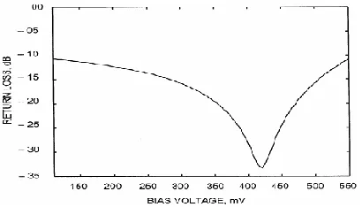
[image:4.612.39.243.165.318.2]IV. Results
Figure 3: VSWR vs bias voltage
The figure 3: shows that how the VSWR is below about 2dB for the bias voltage (100mV to 550mV). And in the same way the return-loss of the antenna is vary as VSWR for different bias voltage.
And the variation of return loss with respect to the bias voltage is shown below.
Figure 4: return-loss in dB vs bias voltage
v. Conclusion
In some application like frequency agile radio, and in radar system a narrow band antenna with tunable frequency is required instead of wide band antenna. Thus for tunable antenna we can use different active loaded devices like Tunnel Diode, Gun Diode. But on the other side
it has also disadvantage, that the dependence of resonance frequency on the co-ordinate of Tunnel Diode, which increases lack of versatility.And one biggest advantage is that the variation of tuning frequency peak by varying the bias voltage, which change the impedance of the patch.
References
[1]K. R. Carver and J. W. Mink, “Microstrip Antenna Technology,” IEEE Transactions on Antennas and Propagation, Vol. 29, No. 1, 1981, pp. 2-24. doi:10.1109/TAP.1981.1142523
[2] D. M. Pozar, “An Update on Microstrip Antenna Theory and Design Including Some Novel Feeding Techniques,”
IEEE Antennas and Propagation Society Newsletter, Vol. 28, No. 5, 1986, pp. 4-9.
[3] J. A. Ansari, R. B. Ram, S. K. Dubey and P. Singh, “A Frequency Agile Stacked Annular Ring Microstrip An-tenna Using Gunn Diode,” Smart Materials and Structures, Vol. 16, No. 6, 2007, pp. 2040-2045. doi:10.1088/0964-1726/16/6/006
[4] P. Bhartia and I. J. Bahal, “Frequency Agile Microstrip Antennas,” Microwave Journal, Vol. 25, No. 10, 1982, pp. 67-70.
[5] G. Kumar and K. C. Gupta, “Broad-Band Microstrip An-tennas Using Additional Resonators Gap-Coupled to the Radiating Edges,” IEEE Transactions on Antennas and Propagation, Vol. 32, No. 12, 1984, pp. 1375-1379. doi:10.1109/TAP.1984.1143264
[6] I. J. Bahl and P. Bhartia, “Microstrip Antennas,” Artech House, Dedham, 1981.
[7] W. F. Woo and. F. Chow, “Principles of Tunnel Diode Circuits,” Wiley, New York, 1969.
[image:4.612.44.249.453.570.2]© 2016, IRJET | Impact Factor value: 4.45 | ISO 9001:2008 Certified Journal
| Page 1340
[9] R. Garg and I. J. Bahal, “Microstrip Discounties,” Inter-national Journal of Electronics, Vol. 45, No. 12, 1978, pp. 81-87. doi:10.1080/00207217808900883