A Power Efficient GDI Technique for Reversible Logic
Multiplexer of Emerging Nanotechnologies
Satish Sharma
Research Scholar ITM University,
Gwalior, India
Shyam Babu Singh
Assistant Professor ITM University,
Gwalior, India
Shyam Akashe
Associate professor
ITM University,
Gwalior, India
ABSTRACT
Reversible logic is becoming one of the best emerging design approaches for future computation of reversible logic having its more application in low power application. This logic is applied in the quantum computers, optical computing, communication and nanotechnology. In reversible logic approach generates the garbage input/output. In this paper design of proposed reversible logic multiplexer with garbage input/output, that the low power, area design technique are using that is the Gate -Diffusion -Input (GDI cell) in this dynamic component of power is reduced, In GDI cell PMOS is not connected to supply voltage VDD and NMOS is not connected to the GND.GDI circuits provide some measure issues of enhanced hazard tolerance and low voltage operation of reversible logic circuits. In this paper propose a novel application of GDI (Gate-Diffusion Input) circuits to Reversible logic multiplexer with its Garbage input and output. The new proposed design technique will consume less power than the other traditional gate. In recent years ago reversible logic circuit is less power dissipation. This GDI cell technique reduces the power of the circuit, delay, Power-Delay Product (PDP) and it also reduced frequency. The device scaling is limited by the power dissipation are more optimize in terms of delay, power supply, frequency , duty cycle, frequency jitter bandwidth of the signal and also demonstrated the noise of the circuit. The proposed reversible logic design. the GDI is effective in low power, low leakage current and lower Delay, The transistor implementation of the proposed gates is done by using Virtuoso tool of cadence. Based on simulation results and analysis at 45 nm technology, some of the trade-offs are made in the design to improve the efficiency.
Keywords
Low Leakage power, GDI technique, delay, (Power-Delay Product) PDP and frequency.
1.
INTRODUCTION
Reversible logic [1] is a very prospective approach of logic synthesis for power reduction in future computing technologies. In a reversible logic circuit, the number of inputs and outputs are same and there is a one-to-one mapping between input and output values. Reversible circuits are constructed using reversible gates. The recent computers erase a bit of information every time they perform a logical operation. Such logical operations are generally known as "irreversible logic". It imposes many design constraints. Zero energy dissipation would be possible only if the network consists of reversible gates. So that reversibility will become an essential property in future circuit design [2]. According to the Landauer [3],
Ebit ≥ ESNL = KBTln2 = 0. 017eV (1) Where, Ebit=the energy required for binary transition,
ESNL=Shannon-von Neumann Landauer (SNL) expression Traditional irreversible hardware computation inevitably leads to energy dissipation due to the loss of each one bit of information which dissipates an amount of 𝐾𝑇 𝑙𝑛(2) Joules of energy, where K is the Boltzmann‟s constant (1.3807×10⁻²³
2.
BASIC CONCEPT OF GATE
DIFFUSION INPUT
The basic concept of GDI cell technique is that shown in figure 1. The PMOS in GDI cell is not connected to the supply VDD and other hand NMOS in GDI cell is not connected to GND. This feature given the GDI cell technique is two extra input pins to use which makes the design are more compatible in terms of no input is increasing the digital circuits. It must be remarked that not all the function are possible in standard P-well process but the most successfully design the CMOS process. One of the major problems of Gate-diffusion input technique requires a special CMOS process that the GDI schemes require twin-well CMOS or silicon on insulator (SOI) process to implement the design more expensive than other standard cell [9]. One of the common basic problems is occurring in GDI cell based logic design low swing of output signals because of the threshold voltage drop across the single channel pass transistor. A simple change in the input configuration of GDI cell based on Boolean function that is different of every function. [10]. The reverse logic multiplexer with garbage input /output is more and the power dissipation in the circuits is less in comparison of the other CMOS logic reversible designs [11]. GDI Technique enables simpler reversible gates; transistor count is less and lower power dissipation in many implementations, as compared with other CMOS design techniques circuits in VLSI Design. The new device can have the basic wide spectrum of implementation in a wide variety of nanotechnology circuits. The Future work of reversible logic multiplexer modeling and simulation of the new Nano devices [12]. Also the basic GDI cell based functional table 1.the function of the F1 and F2 are the complete requirement of logic families. This functionality only F1 is the GDI function that can be realized for the standard P-well CMOS process, because the bulk of any NMOS is equally or constantly biased [13].
[image:2.595.333.537.385.452.2]Fig1. Basic Gate-Diffusion Input cell
Table 1.Truth Table of the basic GDI cell
N P G OUT Function
„0‟ B A ᾹB F1
B „1‟ A Ᾱ+B F2
„1‟ B A A+B OR
B „0‟ A AB AND
C B A ᾹB+AC MUX
„0‟ „1‟ A Ᾱ NOT
3.
BASIC REVERSIBLE LOGIC GATE
A reversible logic gate is n × k logic device where n and k is the number of inputs and outputs with one to one mapping, i.e. and should be equal to k (n = k). A gate is said to be reversible if the input vector can be uniquely recovered from the output vector and there is a one to one correspondence between its input and output logic [13]. A set of reversible logic gates is needed to design reversible logic circuits. An n × k reversible logic gate can be represented as:
𝐈𝐕= (𝐈𝟏, 𝐈𝟐, 𝐈𝟑… … … 𝐈𝐧) (2)
OV= (O1, O2, O3… … … Ok) (3)
Where,Ivand Ov are input and output vectors. Consider the
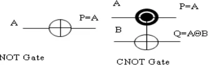
following issues to perform the synthesis of reversible gates and obtain optimization. Any reversible circuit realizes only the function that is reversible. The number of outputs in a reverse gate or circuit has the same as the number of inputs, and generally used traditional NOT gate is the only reverse gate. Every reversible gate has a cost associated with it, called as Quantum cost. The simplest reversible gate is NOT gate and is a 1×1 gate [15]. The Reversible gate 2×2 with quantum cost of the reversible gate having mapping input (A,B) to output (P = A, Q = AB) is shown in Figure 2 that the combinational circuit diagrams of the NOT gate and CNOT gate [16].
Fig 2. Combinational circuit diagram of 1x1 NOT Gate and CNOT Gate
The controlled NOT (CNOT) gate is an example of a 2×2 gate. Many of the available gates are 3×3 Reversible gates such as TR, FG, PG and TG gates. The Quantum Cost of 1×1 Reversible gates is zero, and the Quantum Cost of 2×2 Reversible gates is one. Any reversible gate is optimized by using 1×1 NOT gates (inverter) and 2×2 (Feynman gate) Reversible gates, such as V, V+ (V is the square root of NOT gate and V+ is its Hermitian) and FG gate that is also known
as CNOT gate. The properties of V and V+ Quantum Gates are given in the following equation [17].
[image:2.595.76.257.569.740.2]given more functions [18]. The Delay can be calculated in
reversible logic based on the critical path. It is the longest path that gives the desired output of the system [19]. There exist many reversible gates in the literature.the proposed 3×3 reversible gate with two of its outputw working as 2:1 multiplexer.the gate to used a design of reversible gate circuit with its garbage input and outputs,also design a Reversible half adder and half subtractor circuits.Among them Feynman gate (FG), Peres gate (PG), Toffoli gate (TG) , Fredkin gate (FRG) and Khan Gate (NG) [20] are mostly common. The quantum realizations of all these gates are not available in the literature. Only PG, FG, TG, and FRG have been realized in nanotechnology. A reversible logic circuit should have the following features.
Required least number of reversible gates.
Required least number of constant inputs.
Minimum number of garbage outputs.
The length of cascading gates should be least.
The Same number of outputs as that of inputs.
Hardware complexity that is reducing configuration.
4.
DESIGN AND IMPLEMENTATION
OF
REVERSIBLE
LOGIC
MULTIPLEXER
WITH
GARBAGE
INPUT/OUTPUT
[image:3.595.325.550.69.388.2]The proposed reversible 2:1 multiplexer gate is realized using transistor implementation as described .The required output you can be obtained using only two transistors however, the three transistors are required for calculating garbage outputs. To obtain output G1, a pass transistor is used for passing the selection input S (select) to the output G1 as , when the selected input is 0, the PMOS transistor will be ON while NMOS will be off thus input A is passed to the output Y, if selection input is 1, then the NMOS transistor will be conducting while PMOS is in OFF state, passing input B to the output Y. Similar to output Y, output G2 is passed with input B when S=0 (SEL) and input A, when S=1 [21]. This paper proposed reversible multiplexer gate is proposed in order to function as the 2:1 reversible multiplexer producing two garbage bits. The inputs are A, B and S, it depends on the selected input S, the corresponding information bit is passed on to the output Y in figure 3. In this proposed reversible logic gate circuit applying GDI cell technique that reduces the area of the circuit, low leakage power, delay and Power-delay product (PDP).
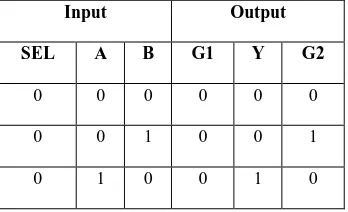
Table 2. Truth table of 2:1 Reversible Multiplexer with garbage input output
Input Output
SEL A B G1 Y G2
0 0 0 0 0 0
0 0 1 0 0 1
0 1 0 0 1 0
0 1 1 0 1 1
1 0 0 1 0 0
1 0 1 1 1 0
1 1 0 1 0 1
1 1 1 1 1 1
Fig 3. Transistor implementation of 2:1 reversible multiplexer with Garbage input/output
Shows the transient response of the circuit with its input, output voltage waveform in terms of transient response time (ns) and it produced no of garbage input/output, that depend on the select input of the circuit of 2:1 reversible logic multiplexer as shown in figure 4. As well as the truth table 2.the wave form show logic level of the reversible logic operation for select input of high and low logic in the operation.
[image:3.595.323.537.526.671.2] [image:3.595.81.255.647.753.2]5.
REVERSIBLE LOGIC FOR LOW
POWER DESIGN
The scaling process variation becoming an important issue for Past few year. The technology is to reach nanometer regime it has resulted in increasing leakage power dissipation [22]. It is important to every design point of view to reduce static power dissipation during the operation. The power reduction is important to achieve without the trade-off in circuit performance. There are several approaches of low power application such as the reduction of supply voltages. Node Capacitance and switching activities. The conventional low power techniques have several challenges with the shrink of CMOS technology sizes, degraded voltage gain, increased speed, increased leakage current and soft error rates [23].the past few years several effective power management design technique have been developed including lowering the supply voltage, low threshold voltage and gating off the clock signal when not in use and designing low power switching functionality of logic gate circuits. These techniques very widely using in industry [24].The multiplexer gate has the largest power consumption because of its complicated XMOS structure and the presence of additional input in GDI cell technique. The GDI cell based gates are more efficient in terms of power, area delay and Power-Delay product (PDP). The results of this reversible logic circuit simulation for power and delay measurement are presented. The GDI technique reduces the dynamic power consumption of the reversible logic circuits in terms of switching Activity and it also reduces the glitches and significantly achieving low power of the reversible operation [25]. The dynamic power measurement in the CMOS circuit at low frequencies was supplied at various supply voltages. The measurements were performed at 0.7 V and the frequency at 40 GHz‟. We hope these results are helpful to further research activities on the GDI technique .The design issue of sequential circuit reversible logic design is currently exploring [26].
6.
RESULT AND DISCUSSION
In this paper all design is based on Gate-diffusion technique. This technique are used to design 2:1 reversible logic multiplexer with garbage input/output and simulated using standard 45 nm CMOS technology and supply voltage 0.7 V at an operating temperature of 27o C. Cadence corporation virtuoso tool of cadence with the specter simulator as IC 6.1 have been used for all design and analysis.
6.1
Leakage Power
The leakage power or static, dynamic Power dissipation is the power dissipated in the circuit when it is in standby mode that is given that the equation below.
𝑃𝑙𝑒𝑎𝑘 = 𝐼𝑙𝑒𝑎𝑘 × 𝑉𝐷𝐷 (7)
Where Ileak is the leakage current that flow in the transistor
when it is in off state and supply voltage VDD.
Leakage current consist various components of the current. Such as the sub threshold leakage, gate leakage, reverse biased junction leakage, gate induced drain leakage, these sub threshold leakage and the gate leakage are dominant in the circuit [27]. The sub threshold leakage current of a MOS device can be given by form of below.
𝐼𝑑𝑠 = 𝐼𝑑𝑠𝑜𝑒
𝑉𝐺𝑆 −𝑉𝑇
𝑛ʋ𝑇 [1 − 𝑒𝑉𝐷𝑆
𝑉𝑇] (8)
𝐼 = 𝜇 ∁ (𝑊)𝑉2 (9)
Where Off is the charge carrier mobility off state, Cox is the
gate capacitance oxide per unit area, the length is Bandwidth of the channel is L, Vt is the threshold voltage, VT is the
thermal voltage, and is the sub threshold voltage swing Coefficients, VGS is the gate to source voltage of transistor and
VDS drain to source voltage. This technique is tested in
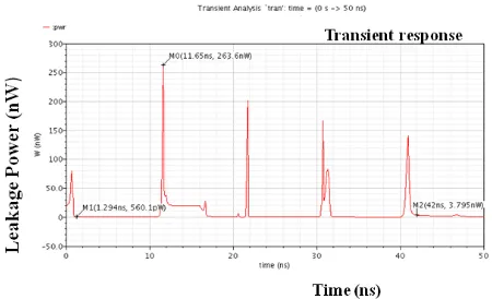
proposed reversible logic multiplexer circuit with the garbage input/output. The figure 5,6 shows the Average power 263.9 (nW), Leakage power 5.266 (nW), Leakage current 471.9 (a) , delay 11.18 (ns) and Power-Delay Product (PDP) 2.947×10⁻²¹ (J) at 45 nm technology and supply Voltage 0.7 V and the compare these results with 180 nm technology at the supply voltage is 1.8V that are the Average power 309.5 (nW), Leakage power 1.831 (nW), Leakage current 783.9 (a), Delay 11.25 (ns) and Power-Delay product (PDP) 3.478×10⁻²¹ (J).the paper research is delay is decrease and low leakage power in compare to the CMOS based logic circuits. The figure 7 shows the response of the RMS noise of the circuit that gives the value with 1.953×10⁻⁸ (v/sqrt Hz), Phase Margin 36.03
(dB), Peak noise 1.035×10⁻⁹ dB.
The Average power dissipation is determining the circuit
.
𝑃𝑎𝑣𝑔 = 𝐶 𝑉𝐷𝐷2 𝑓𝐶𝐿𝐾 (10) Pavg =Average power dissipation, C=Load capacitance,Fc=clock frequency, VDD=supply voltage
Fig 5. Simulated leakage Current Response of the
Reversible Logic Multiplexer with its Garbage
[image:4.595.318.544.343.495.2]input/output using the GDI cell technique
[image:4.595.319.544.544.681.2]Fig 7. Simulated RMS Noise Response of the Reversible Logic Multiplexer with its Garbage input/output using the GDI cell technique
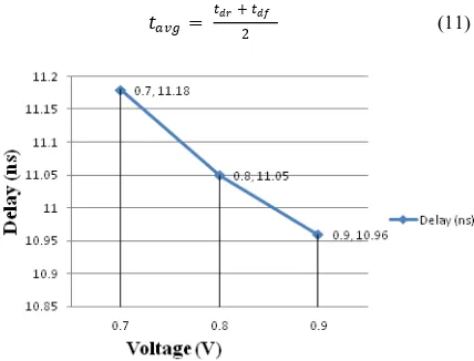
The graph 8 shows the propagation delay of the reversible logic multiplexer using GDI cell technique. The voltage of the circuit varies from 0.7V to 0.9V that varying the graph of delay at 45 nm technology. The delay is decade according to supply voltage when increasing the threshold voltage of the circuit the delay of the circuit is decreasing. The power of the circuit is also depends on the channel length of the NMOS and PMOS.When apply the various threshold voltage at 45 nm technology, that time determine the power response of circuit. When increasing the channel length of the circuit power is also increasing. If reduce the channel length of the circuit it decreases according to channel length and delay is increasing but power is low and the PDP is also varying that shown in figure below.
Then the average gate delay for rising and falling transition is. 𝑡𝑎𝑣𝑔=
𝑡𝑑𝑟 + 𝑡𝑑𝑓
2 (11)
Fig 8. Simulated Graph delay verses various voltages of the Reversible Logic Multiplexer with its Garbage input/output using the GDI cell technique
Fig 9. Simulated Graph Power verses various channel lengths of the Reversible Logic Multiplexer with its Garbage input/output using the GDI cell technique
The graph 9, 10 of reversible logic based GDI cell simulation result of various parameters like leakage current (nA), Average power (nW) and leakage power (nW) comparing the result at 45 nm and 180 nm technology. The Power-Delay Product of the circuit has shown the percentage of 180 nm technology is 54% and the in 45 nm technology the Power- Delay Product (PDP) at the 46 %of the supply voltage 0.7 V. Shown in figure below 11.
Fig 10. Simulated Graph various parameter leakage Current (nA),Average Power(nW) and Leakage Power(nW) of the Reversible Logic Multiplexer with its Garbage input/output using GDI cell Technique
6.2
Power delay ProductPower delay Product is independent of switching frequency and can be calculated
[image:5.595.323.548.78.223.2] [image:5.595.62.281.80.217.2] [image:5.595.326.539.370.497.2] [image:5.595.63.277.430.593.2]Fig 11. The Power-Delay-Product Comparison Graph of Two Technology 180 and 45 nm Reversible Logic Multiplexer with its Garbage input/output using GDI cell Technique
6.2
Duty cycle
PPave
p =
PW
T = PW × PRF = PW
PRI= duty cycle (13)
Pp =peak power, Pave =average power, PRF=pulse Repletion
frequency, PW=pulse width, PRI=pulse Repetition interval.
6.3
Frequency
Frequency 𝐟 =𝟏𝐓T=time interval, f=frequency (14)
6.4
Settling Time
Settling time is defined as in terms of various values that is the Tm as Td approaches zero. A Sufficient and fix value of Tt
is obtained. if Td is less than 50 ns.
𝑇𝑚≈ 𝑇2𝑑+ 𝑇2𝑡 (15)
𝑇𝑑≈ 𝑇2𝑚− 𝑇2𝑡 (16) Where Tm is the observed settling time when measuring a
settling time Td and Tt is the settling time of test circuit.
Voltage gain = 𝑉𝑉𝑜𝑢𝑡
[image:6.595.74.259.415.734.2]𝑖𝑛 (17)
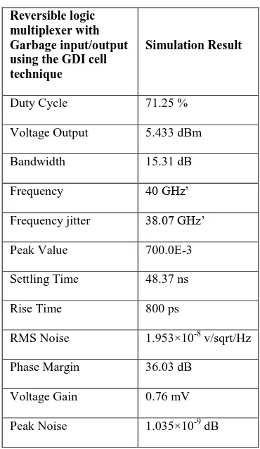
Table 3. Various Simulation results of 2:1 Reversible Multiplexer with garbage input/ output using GDI cell techniques based on Cadence tool
Reversible logic multiplexer with Garbage input/output using the GDI cell technique
Simulation Result
Duty Cycle 71.25 %
Voltage Output 5.433 dBm
Bandwidth 15.31 dB
Frequency 40 GHz‟
Frequency jitter 38.07 GHz‟
Peak Value 700.0E-3
Settling Time 48.37 ns
Rise Time 800 ps
RMS Noise 1.953×10⁻⁸ v/sqrt/Hz Phase Margin 36.03 dB
Voltage Gain 0.76 mV Peak Noise 1.035×10⁻⁹ dB
Table 4. Various Simulation results of 2:1 Reversible Multiplexer with garbage input/ output using GDI cell techniques based on Cadence tool
Tech. (nm)
Volta-ge (V)
Leakag e Current (nA)
Total Averag e Power (nW)
Leakage Power (nW)
Delay (ns)
PDP (J)
45 0.7 471.9 263.9 5.266 11.18
2.94 7×10
-21
180 1.8 783.9 309.5 1.831 11.24
3.47 8×10
-21
7.
CONCLUSION
These papers elucidate a novel reversible gate and the design of reversible multiplexer like 2:1using the proposed reversible gate is discussed. The table demonstrates and compares the two technologies. The result of the proposed design shows that the circuits are more optimized in terms of delay, power supply (0.7V), Power Delay Product and voltage gain. The GDI technique based result also show the other hand RMS Noise, duty cycle, Peak Noise, Phage margin and bandwidth of the signal. This paper reduces the delay, low leakage power in the reversible operational circuit. This Research paper focus on power and calculate the result in two technologies 180 and 45 nm and compared leakage power, decreases delay in 45 nm in comparison 180 nm PDP result was shown in previous table. The GDI cell technique is the most effective technique for reducing the power consumption, delay, Leakage Power, leakage current of the circuit. It shows the 46 % reduction of the Power-Delay-Product (PDP).the paper is also demonstrates the noise free desire circuit in future point of view. Since the reversible circuits are based on pass transistors, there is a problem occurs of loss the information after passing through a number of stages. This problem can be fixed with static CMOS inverter insertion or other level restoring techniques. The proposed reversible multiplexer has a high performance as compared to other reversible circuit. This proposed reversible circuit is a design using nanotechnology. The other power reduction technique is performing the less computation in comparison of GDI cell technique.
8.
ACKNOWLEDGMENTS
This work is supported by ITM University, Gwalior in collaboration with Cadence Design System, Bangalore India.
9.
REFERENCES
[1] T. Toffoli., “Reversible Computing,” in Automata, Languages and Programming, J. W. Baker and J. Van Leuven, ED. Springer Verlag, 1980, pp. 632-644. [2] H. Bennett, “Logical reversibility of computation,” IBM
14 [3] Landauer, R., 1961. Irreversibility and heat generation in
the computing process, IBM J. Research and Development, 5 (3): 183‐191.
[4] Prathyusha Konduri Pobbireddy Sameera Pavan Kumar. V “ Performance Analysis of D Flip-Flop Implemented in GDI and ACPL Low power Design Techniques” INTERNATIONAL JOURNAL OF ADVANCED ENGINEERING SCIENCES AND TECHNOLOGIES ISSN 2230-7818 Vol No. 5, Issue No. 2, 177 – 183,2011. [5] Po-Ming Lee, Chia-Hao Hsu, and Yun-Hsiun Hung
“Novel 10-T full adders realized by GDI structure” [6] M. P Frank, “Introduction to reversible computing:
motivation, progress, and challenges”, Proceedings of the 2nd Conference on Computing Fron-tiers, 2005, pages 385–390.
[7] Md. Sazzad Hossain, Md. Rashedul Hasan Rakib, Md. Motiur Rahman,et.all “ANEW DESIGN TECHNIQUE OF REVERSIBLE BCD ADDER BASED ON NMOSWITH PASS TRANSISTOR GATES”
[8] Vlatko Vedral, Adriano Bareno and Artur Ekert, “Quantum Networks for Elementary Arithmetic Operations”, arXiv: quantph/ 9511018 v1, Nov 1995. [9] Deependra Sharma “design of low power CMOS cell
structures based on Gate Diffusion input technique” July 2010.
[10] T. Kalavathidevi and C. Venkatesh “Gate Diffusion Input (GDI) Circuits Based Low Power VLSI Architecture for a Viterbi Decoder” IRANIAN JOURNAL OF ELECTRICAL AND COMPUTER ENGINEERING, VOL. 10, NO. 2, SUMMER-FALL 2011,1682-0053/11$20 © 2011 ACECR, pp 77.
[11] Pavan kumar Reddy S, Mrs. N. SARASWATHI, Gnanavargin Rokkala “ ULTRA LOW POWER MODULO 2n+1 MULTIPLIER USING GDI” IJCER | Mar-Apr 2012 | Vol. 2 | Issue No.2 |449-456 Page 449. [12] Anas N. Al-Rabadi “Carbon Nano Tube (CNT)
Multiplexers for Multiple-Valued Computing”, FACTA UNIVERSITATIS (NIˇS ) SER.: ELEC. ENERG. Vol. 20, no. 2, August 2007, 175-186.
[13] T. Kalavathidevi and C. Venkatesh. “Gate Diffusion Input (GDI) Circuits Based Low Power VLSI Architecture for a Viterbi Decoder” IRANIAN JOURNAL OF ELECTRICAL AND COMPUTER ENGINEERING, VOL. 10, NO. 2, SUMMER-FALL 2011.
[14] Mohammad Assarian, Majid Haghparast and Keivan Navi “Delay Reduction in Optimized Reversible Multiplier Circuit”, Research Journal of Applied Sciences, Engineering and Technology 4 (1): 27-32, 2012 ISSN: 2040-7467 ©Maxwell Scientific Organization, 2012, Submitted: August 26, 2011 Accepted: September 30, 2011, Published: January 01, 2012.
[15] Ravish Aradhya H V, Muralidhara K N, Praveen Kumar B V “DESIGN OF LOW POWER ARITHMETIC UNIT BASED ON REVERSIBLE LOGIC”, International Journal of VLSI and Signal Processing Applications, Vol. 1, Issue 1 (30- 38), ISSN 2231-3133.
[16] B. Raghu Kanth, B.Murali Krishna,G. Phani Kumar “ A COMPARITIVE STUDY OF REVERSIBLE LOGIC GATES”, International Journal of VLSI & Signal Processing Applications, Vol.2,Issue 1, Feb 2012, (51-55), ISSN 2231-3133 ( Online)
[17] Ravish Aradhya H V, Praveen Kumar B V, Muralidhara K N “Design of Control unit for Low Power ALU Using Reversible Logic” International Journal of Scientific & Engineering Research, Volume 2, Issue 9, September-2011 1 ISSN 2229-5518.
[18] Saurabh Kotiyal, Himanshu Thapliyal and Nagarajan Ranganathan “Mach-Zehnder Interferometer Based All Optical Reversible NOR Gates”, 2012 IEEE Computer Society Annual Symposium on VLSI, 978-0-7695
4767-1/12 $26.00 © 2012 IEEE, DOI
10.1109/ISVLSI.2012.72.
[19] Jie Ren and Vasili K. Semenov “Progress With Physically and Logically Reversible Superconducting Digital Circuits”, IEEE TRANSACTIONS ON APPLIED SUPERCONDUCTIVITY, VOL. 21, NO. 3, JUNE 2011.
[20] Pallav Gupta, Student Member, IEEE, Abhinav Agrawal, and Niraj K. Jha, Fellow, IEEE “An Algorithm for Synthesis of Reversible Logic Circuits”, IEEE TRANSACTIONS ON COMPUTER-AIDED DESIGN OF INTEGRATED CIRCUITS AND SYSTEMS, VOL. 25, NO. 11, NOVEMBER 2006.
[21] Praveen‟s, Vinay Kumar S.B 2n:1 Reversible Multiplexer and its Transistor Implementation IJCER | Jan-Feb 2012 | Vol. 2 | Issue No.1 |182-189 Page 182. [22] Kanak Agarwal, Harmander Deogun, Dennis Sylvester,
Kevin Nowka “Power Gating with Multiple Sleep Modes”, This work was supported in part under Defense Advanced Research Project Agency Contract F33615-030C-4106.
[23] Jianping Hu, and Xiaolei Sheng “A Single-Phase Register File with Complementary Pass-Transistor Adiabatic Logic” , World Academy of Science, Engineering and Technology 38 2010.
[24] Conrad H. Ziesler, Joohee Kim, and Marios C. Papaefthymiou “Energy Recovery Design for Low-Power ASICs”.
[25] M. K. Akbari and A. Jahanian, "Area efficient, low power, and robust design for add compare and select units," in Proc. of the IEEE Conf. on EUROMICRO Systems on Digital System Design, DSD'04, pp. 611-614, Sep. 2004.
[26] Arkadiy Morgenshtein, Alexander Fish, and Israel A. Wagner “Gate-Diffusion Input (GDI): A Power-Efficient Method for Digital Combinatorial Circuits”, IEEE TRANSACTIONS ON VERY LARGE SCALE INTEGRATION (VLSI) SYSTEMS, VOL. 10, NO. 5, OCTOBER 2002.