© 2018, IRJET | Impact Factor value: 6.171 | ISO 9001:2008 Certified Journal | Page 3922
Design of 8 bit Analog to Digital Converter (ADC) in 45 nm CMOS
Technology
Harshit Baranwal
1, Jadhav Abhijit Kaluram
2, Vivek kushwaha
3, Prashant Avhad
41,2,3
Dept. of E&TC Engg. Dr. D Y Patil College of Engineering, Ambi, Pune, India
4
Assistant Professor, Dept. of E&TC Engg. Dr. D Y Patil College of Engineering, Ambi, Pune, India
---***---Abstract
-
In the current technological world, the technology advancement leads most of the application demanding for a reduction in total size of the system in terms of space the space they occupied in any device. The Data converter section, besides being very power demanding and it is also usually extremely power demanding in comparison with other blocks of any architecture and that’s why low power has also become a tough requirement in most of the system being maintained in a low figure has almost become a mandatory specification in many application. In this thesis work we have chosen the SAR control logic architecture as it one of the very successful moderate resolution achievable converter system available among all the data converter control logic architecture. Initially we encounter the different types of SAR control logic and focuses on selection of suitable comparator architecture and SAR Control Logic and DAC based on this analysis, dynamic two-stage comparator, SAR Control Logic and BWC Capacitive Array as DAC is selected due to its energy efficiency and capability of working in low supply voltages and consume Low Power and the schematic model of the entire system will try to implement using EDA tool Microwind 3.5 and DSCH in order to fulfil the technical requirement of the project.Key Words: SAR, ADC, EOC, DAC, S/H
1. INTRODUCTION
Although in now continually changing technological world as all the electronics components are goes tiny day by day and large numbers of devices and micro-controllers are coming everyday it is necessary for all the supporting component of the devices and micro- controller to be fitted as per their requirement and specifications. In order to follow the trend of new technologies to become tiny and to be the better then the previous version and updating the old version with the new it is also essential for the Analog to Digital comparator to update themselves as per the trends. As per the previous fabrication technique all the Analog to Digital converters are mostly fabricated with the foundry of 120 nanometer technic and above than 120 nanometer i.e. 180nanometer etc. So in order to adapting the new technological revolution Analog to Digital converter also have to fabricate on lower scale than its previous foundry and in order to getting this we are going to design the Analog to Digital Converter with lower scale than 120 nanometer, which is 45 nanometer. In this work we studied the each block diagram of ADC and construct these with the help of EDA tool. In order to so we started with the Comparator block diagram and studied the different type of Architecture of comparator i.e. open loop comparator, Latch
comparator and Dynamic latch Comparator but we found that dynamic latch comparator introduces less delay and low power consumption so we further studied the different type of comparator i.e. N-type latched comparator, dynamic two stage latched comparator and modified two stage latched comparator and we also simulate these using different kind of Set-Reset latch i.e. NAND SR latch and NOR SR latch and on the basis of result we found that dynamic two stage comparator has low power consumption along with the low delay and then after that we proceed with the SAR control logic and we had the two methods for design the SAR logic and on the basis of previous work we found that SAR control logic proposed by Anderson consume the less power and we proceeds with this logic and we select the Binary Weighted Capacitor array over the resistive array as our DAC functional block among the Two stage weighted capacitor array and C-2C capacitor array as it also has the low power consumption which is our first priority. All these schematic architecture were simulated using the EDA tool Microwind and DSCH in the 45 nanometer foundry and after inserting these functional block diagram we further construct the functional Analog to Digital Converter.
2. Implementation of ADC
2.1 Comparator Implementation
© 2018, IRJET | Impact Factor value: 6.171 | ISO 9001:2008 Certified Journal | Page 3923
[image:2.595.43.280.254.394.2]Fig. 1: Power Consumption Comparison
Fig 2: Time Delay Comparison
Since the Priority is the Power Consumption and Time Delay, Dynamic two stage Latched Comparator with the NOR latch Consumes minimum power and it has the lowest Time delay as shown in the figure 1 and 2 so in the fabrication of 8 bit Analog to Digital Comparator we used the Dynamic two stage latched comparator.
2.2 SAR Control Logic Implementation
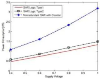
[image:2.595.313.551.275.427.2]We found two different type of approaches to designing the SAR logic. The first one is proposed by Anderson consists of a ring counter and a shift register. At least 2N flip flops are employed in this kind of SAR [16]. The other, which is proposed by Rossi, contains N flip flops and some combinational logic [17]. As Anderson’s Proposed method consist of a ring counter and a shift register and Non redundant SAR logic consists a combinational logic and flip flops but the logic proposed by Anderson has the low Power consumption[18] as explained in figure 3 [18].
Figure 3 SAR Comparison of Average power vs. scaled supply voltage[18] Since our priority is about Low Power Consumption so we consider the type 1 SAR logic which is proposed by the Anderson. The SAR architecture proposed by the Anderson is explained in the figure 4
Fig 3: SAR Comparison of Average power vs. scaled supply
voltage[18]
Fig 4:SAR Architecture
We implement the SAR Control logic using the EDA tool DSCH and Microwind and simulate it and its simulation is stated below in figure 5 and it has the power consumption of 12.067μW.
Fig 5: SAR Simulation Waveform
2.3 DAC Implementation
[image:2.595.310.559.527.656.2]© 2018, IRJET | Impact Factor value: 6.171 | ISO 9001:2008 Certified Journal | Page 3924
Fig 6: DAC schematic View
The Output of the DAC is defined by the equation described below:
The linearity of ADC is restricted by the linearity of the DAC which is caused by the capacitor mismatch. Therefore, choosing an appropriate value for the unit capacitance is vital. Reducing the unit capacitance value improves the linearity but deteriorates the noise performance at the same time due to KT/C thermal noise. The minimum value of the unit capacitor is limited by several factors including KT/C thermal noise, capacitor matching and the value of the parasitic capacitances [21].A unit capacitance of 20fF is chosen in this design. The values of the other capacitors in the capacitor array are defined based on the unit capacitance.
3. Performance Evolution
We studied two different types of architecture of SAR Analog to Digital Comparator i.e. Separate Sample and Hold Circuit and Charge Redistribution Architecture of ADC but the main drawback of ’Separate DAC and Sample and Hold circuit ADC’ is that it consume more power due to separate Sample and Hold circuit and as our concern is about the low power consumption we can not use this design and we moved to the ’Charge Redistribution Architecture ADC’ which has a different approach as this architecture encompasses a capacitive DAC which also operates as a sample and hold circuit.
[image:3.595.40.290.83.233.2]Figure 7 represents the test bench for ADC performance measurement.
Fig 7: SAR ADC test bench
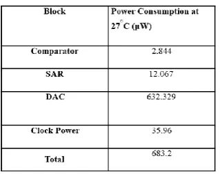
We first design the high level schematic of the SAR ADC using the charge redistribution architecture and further replace the blocks by the chosen schematic circuits and construct the ADC using EDA tool Microwind and DSCH. The ADC is simulated with VDD= 1V , VREF =VCM = 0.5V, and clock period of 4ns and sample frequency of 500MHz and The input signal is a full swing sinusoidal with fin= 250MHz. We simulate results under 27◦C and the total power consumption is of 683µW.
DAC consumes the largest amount of power among other blocks which is 92.5%. As discussed above, the unit capacitance in the DAC is chosen to be 20 fF. After DAC, SAR control logic with 1.766%, clock power consume 5.26% and comparator with 0.41% consumes the largest amount of power respectively.
4. Conclusion
[image:3.595.355.515.382.508.2]© 2018, IRJET | Impact Factor value: 6.171 | ISO 9001:2008 Certified Journal | Page 3925 SAR control logic is significantly reduced and consumes only
1.766% of the total power. The design of comparator is also a crucial part of ADC design In this work, comparator performance metrics as well as several types of comparators are studied, such as open loop comparator, pre-amplifier preceding a latch comparator, and dynamic comparator. Based on these studies, dynamic comparators consume lower power compared to the other approaches. Therefore, diverse architectures of dynamic comparators are implemented and compared regarding power consumption, speed, and accuracy. Consequently, the dynamic two-stage comparator is selected to be used in the designed ADC.
REFERENCES
[1]Kent. H. Lundsberg, Analog-to-Digital Converters Testing, 2002.
[2] Nicholas ”Nick” Gray, ABCs of ADCs, 2003 National Semiconductor Corpora- tion.
[3] A. Anand Kumar, Fundamentals of Digital Circuit.
[4] Abhijan Chakravarty & Sambhav Jain, Measure an ADC’s offset and gain error, EDN Network, May 01, 2014.
[5] W.-Phillip E. Allen and Douglas R. Holberg, CMOS Analog Circuit Design. Oxford University Press, 2nd Edition, New York, 2003.
[6]A. Rodriguez-Perez, M. Delgado-Restituto, and F. Medeiro, ”Power efficient ADCs for Biomedical Signal Acquisition,” IMSE-CNM and University of Seville.
[7] B. Razavi, Principles of Data Conversion System Design, Wiley- Interscience, IEEE Press, 1995.
[8]Y. S. Yee, L. M. Terman, and L. G. Heller, ”A Two-Stage Weighted Capacitor Network for D/A,A/D Conversion,” IEEE Journal of Solid- State Circuits, vol. SC-14, pp. 778?781, August 1979.
[9] J. L. McCreary and P. R. Gray, ”All-MOS Charge Redistribution Analog- to- Digital Conversion Techniques-Part I,” IEEE Journal of Solid-State Circuits, vol. SC-10, no. 6, December 1975.
[10] H.Khurramabadi ADC Converters (Lecture 21). UC Berkeley Course, Analog- Digital Interfaces in VLSI Technology EE247. 2006
[11] J. Cranninckx and G. Van der Plas, ”A 65fJ/ conversion-step 0-to-50MS/s. 0-to-0.7mW 9b ChargeSharing SAR ADC in 90nm Digital CMOS,”ISSCC Dig.Tech.Papers, Feb. 2007.
[12]H. Jeon, ”Low-Power high-speed low-offset fully dynamic CMOS latched com- parator,” Northeastern University, 2010.
[13] Pedro M. Figueiredo and Joao C. Vital, ”Kickback Noise Reduction Techniques for CMOS Latched Comparators,” IEEE Transactions on Circuits and Systems, vol.53, no.7, July 2006.
[14]L. Cong, ”Pseudo C-2C Ladder-Based Data Converter Technique,” IEEE Transac- tions on Circuits and Systems, vol. 48, no. 10, October 2001.
[15] M. Van Elzakker, E. van Tuijl, P. Geraedts, D. Schinkel, E. Klumperink and B. Nauta, ”A 1.9?W 4.4fJ/Conversion-step 10b 1MS/s Charge- Redistribution ADC,” ISSCC Dig. Tech. Papers, Feb. 2008.
[16] T.O. Anderson, ”Optimum Control Logic for Successive Approximation Analog- to-Digital Converters,” Computer Design, vol. 11, no. 7, pp. 81- 86, 1972.
[17] A. Rossi and G. Fucili, ”Nonredundant successive approximation register for A/D converter,” Electronics Letters, vol.32, no.12, pp.1055- 1057,1996.
[18]A Study of Successive Approximation Registers and Implementation of an Ultra- Low Power 10-bit SAR ADC in 65nm CMOS Technology by Raheleh Hedayati
[19] H. Jeon, ”Low-Power high-speed low-offset fully dynamic CMOS latched com- parator,” Northeastern University, 2010.
[20] S. T. Oskuii, ”Comparative Study on Low-Power High-Performance Flip-Flops, Master thesis, Linkoping University, 2003.
[21] M. Saberi, R. Lotfi, K. Mafinezhad, W. A. Serdijn, ”Analysis of Power Consump- tion and Lineary in Capacitive Digital-to-Analog Converters Used in Successive Approximation ADCs,” IEEE Transactions on Circuits and Systems, vol. 58, no. 8, August 2011.
[22] J. M Rabaey, A. Chandrakasan , and B. Nikolic, Digital Integrated Circuits ? A Desigsn Perspective, Prentice Hall, 2nd edition, 2003.
[23] D. Zhang, ”Design and Evaluation of an Ultra-Low Power Successive Approxi- mation ADC,” Master thesis, Linkoping University, 2009.
[24] D. Zhang, A. K. Bhide, and A. Alvandpour, ”Design of CMOS Sampling Switch for Ultra-Low Power ADCs in Biomedical Application,” in proceedings of the 28th Norchip conference IEEE,Nov.2010.
© 2018, IRJET | Impact Factor value: 6.171 | ISO 9001:2008 Certified Journal | Page 3926
Jadhav Abhijit Kaluram
E&TC ENGG. Department
Dr. D Y Patil College of Engineering Ambi, Pune, Maharashtra
India
Harshit Baranwal
E&TC ENGG. Department
Dr. D Y Patil College of Engineering Ambi, Pune, Maharashtra
India
Vivek Kushwaha
E&TC ENGG. Department
Dr. D Y Patil College of Engineering Ambi, Pune, Maharashtra
India
Prof. Prashant Avhad
Asst. Professor
E&TC ENGG. Department
Dr. D Y Patil College of Engineering Ambi, Pune, Maharashtra