International Journal of Emerging Technology and Advanced Engineering
Website: www.ijetae.com (ISSN 2250-2459, ISO 9001:2008 Certified Journal, Volume 3, Issue 7, July 2013)
76
Ultra Low Power Logic Gates
N K Kaphungkui
Dept. Of ECE, Dibrugarh University, Assam, India
Abstract— In this work, implementation of all the basic
logic gates is presented using 180nm CMOS technology with a very low voltage of 0.7V. Ideally logic family should not dissipate power, have zero propagation delay, controlled rise and fall times with noise immunity. The property of CMOS closely approaches these characteristics. Another desirable characteristic of CMOS are its robustness with respect to voltage and size scaling. Though with all the desirable characteristics of CMOS when it is implemented in the field of VLSI design there is always a tradeoff between area, power dissipation and speed of operation. The main objective of this paper is to implement all the basic logic gates by exploiting the property of voltage and Gate size scaling of CMOS with ultra low power dissipation without affecting the normal operation of the basic gates. In IC technology which is powered by battery, if the total power dissipation is low, the service time offer by the battery is much longer.
Keywords – CMOS, Dynamic Power, Logic family, Static
Power, Universal Gate, W/L ratio.
I. INTRODUCTION
In IC design technology where numbers of logic gates are integrated, constant and continuous works is being carried out by different experts to reduce the power dissipation. It is still a big challenge for researchers to design a reliable circuit with very low power dissipation. There are different approaches to minimize the power dissipation base on architecture, circuit level, layout, and process technology. Among all these techniques, at the circuit design level considerable amount of power savings can be achieve by means of proper choice of a logic style for implementing combinational circuits. This is because all the important parameters governing power dissipation— switching capacitance, transition activity, and short-circuit
currents arestrongly influenced by the chosen logic circuit
[1]. Another approach to reduce power dissipation is by
using stack technique where each of the NMOS and PMOS in the logic gate is split into two transistors [2]. Sub threshold circuit design operation technique also reduces power dissipation in CMOS where circuits should be operated in near-threshold region [3]. Another effective way is by reducing the supply voltage as CMOS total power dissipation depends upon two power i.e. dynamic power and static power. As these both power depends upon
VDD if supply voltage is reduced the total power can be
minimize.
The main aim of this paper is to reduce the power dissipation of logic gates by voltage reduction technique.
II. GENERAL REVIEW OF TOTAL POWER CONSUMPTION IN
CMOS.
The basic equation governing the total power in CMOS circuit is given by
PTotal = PDynamic + PStatic
PTotal = ½ CLVDD2𝒶f + IScVDD + IStaticVDD (1)
Where CL is the load capacitance, f is the frequency of
operation, 𝒶 is the activity factor, ISc is the short circuit
current [3] [4]. The equation (1) implies that both the dynamic and static power depends upon the supply voltage
VDD at large. The dynamic power consumption is mainly
due to the charging and dis-charging of the capacitance and short circuit current. A short circuit current flows when the pull up and pull down networks in a CMOS circuit are simultaneously on and a direct path exists between the supply line and ground. Dynamic power is directly proportional to the square of the supply voltage. Therefore, dynamic power reduces in a quadratic manner when the
supply voltage isreduced. Leakage power is dependent on
the leakage current flowing in the CMOS circuit. If the
supply voltage VDD is reduced the total power dissipation in
the CMOS circuit can be decrease tremendously. This work
is carried out atsupply voltage of 0.7V with 180nm CMOS
technology by scaling the size of MOS transistor to its
minimum optimum level so that the basic gate operation is not affected.
III. CIRCUIT IMPLEMENTATION
The implementation of logic family include universal
logic gates (NAND gate, NOR gate) and basic gates such as OR gate (implementing with NOR gate), AND gate (implementing with NAND gate), XOR gate and XNOR
gate. Simulation is carried out with a supply voltage VDD of
International Journal of Emerging Technology and Advanced Engineering
Website: www.ijetae.com (ISSN 2250-2459, ISO 9001:2008 Certified Journal, Volume 3, Issue 7, July 2013)
77
The W/L ratios of each gate are preciously optimized for proper operation without affecting the basic Gate operation.
(a). NAND GATE
[image:2.612.338.541.117.284.2]If any one of the input of NAND Gate is logic 0 the output is always high as shown in the simulation result Fig 1 (a). To simulate the gate, bit of stream (010010) is gave to input A and (010110) to input B. C is the output with bit stream (101101). With four transistors NAND gate in Fig.1 is implemented and the total power dissipation from this gate is only 8.36 pW which is the lowest among all the Gates. The operation table of NAND gate is also shown in Table I.
Fig.1 NAND GATE
Table I NAND GATE OPERATION TABLE
0 1 00 2 00 3 00 4 00 5 00 6 00 7 00 8 00 9 00
T im e (n s )
- 100 - 0 1 00 2 00 3 00 4 00 5 00 6 00 7 00 8 00
V
o
lt
a
g
e
(m
V
)
v( c) nand
0 1 00 2 00 3 00 4 00 5 00 6 00 7 00 8 00 9 00
T im e (n s )
0 1 00 2 00 3 00 4 00 5 00 6 00 7 00
V
o
lt
a
g
e
(m
V
)
v( b) nand
0 1 00 2 00 3 00 4 00 5 00 6 00 7 00 8 00 9 00
T im e (n s )
0 1 00 2 00 3 00 4 00 5 00 6 00 7 00
V
o
lt
a
g
e
(m
V
)
v( a) nand
Fig.1 (a) Simulation result of NAND Gate
(B). NORGATE
[image:2.612.79.258.278.599.2]When one of the input to NOR Gate is logic 1 the output is always logic 0. The condition for NOR Gate output to go high is when all the inputs are logic 0. NOR Gate is the complement of OR gate. NOR Gate is implemented with four transistors as shown in Fig. 2. The power dissipate from this Gate is 33.5 pW with the circuit current of 47.86 pA only. The input output result and its simulation results is shown in Table II and Fig 2. (a) Respectively. Input A and B are bits (010001) and (010101). C is the resultant output with bit stream (101010)
Fig. 2 NOR GATE
[image:2.612.362.526.413.587.2]International Journal of Emerging Technology and Advanced Engineering
Website: www.ijetae.com (ISSN 2250-2459, ISO 9001:2008 Certified Journal, Volume 3, Issue 7, July 2013)
[image:3.612.343.543.116.385.2] [image:3.612.70.266.146.395.2]78 Table II
NOR GATE OPERATION TABLE
0 1 00 2 00 3 00 4 00 5 00 6 00 7 00 8 00 9 00
T im e (n s )
- 100 - 0 1 00 2 00 3 00 4 00 5 00 6 00 7 00 8 00
V
o
lt
a
g
e
(m
V
)
v( c) nor
0 1 00 2 00 3 00 4 00 5 00 6 00 7 00 8 00 9 00
T im e (n s )
0 1 00 2 00 3 00 4 00 5 00 6 00 7 00
V
o
lt
a
g
e
(m
V
)
v( b) nor
0 1 00 2 00 3 00 4 00 5 00 6 00 7 00 8 00 9 00
T im e (n s )
0 1 00 2 00 3 00 4 00 5 00 6 00 7 00
V
o
lt
a
g
e
(m
V
)
v( a) nor
Fig.2 (a) Simulation Result of NOR Gate
(c). OR GATE
[image:3.612.74.262.563.695.2]When either of the input to OR Gate is logic 1 the output is always logic 1. This gate is implemented with one of the universal gate i.e with NOR gate as shown in Fig.3. Four NMOS and four PMOS are required to construct OR Gate. The total power dissipated from this gate is 43.17 pW with a circuit current consumption of 61.66 pA. The operation of OR Gate and its simulation result is also shown below in Table III and Fig. 3 (a) respectively. Stream of bits (01010101) and (01000100) are input A and B. C is the resultant output with bits (01010101)
Fig.3 OR GATE
Table III OR GATE OPERATION TABLE
0 .0 0 .1 0 .2 0 .3 0 .4 0 .5 0 .6 0 .7 0 .8 0 .9 1 .0 1 .1 1 .2
T im e (u s )
0 1 00 2 00 3 00 4 00 5 00 6 00 7 00
V
o
lt
a
g
e
(m
V
)
v( c) or
0 .0 0 .1 0 .2 0 .3 0 .4 0 .5 0 .6 0 .7 0 .8 0 .9 1 .0 1 .1 1 .2
T im e (u s )
0 1 00 2 00 3 00 4 00 5 00 6 00 7 00
V
o
lt
a
g
e
(m
V
)
v( b) or
0 .0 0 .1 0 .2 0 .3 0 .4 0 .5 0 .6 0 .7 0 .8 0 .9 1 .0 1 .1 1 .2
T im e (u s )
0 1 00 2 00 3 00 4 00 5 00 6 00 7 00
V
o
lt
a
g
e
(m
V
)
v( a) or
Fig.3 (a) Simulation Result of OR Gate
(d). AND GATE
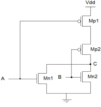
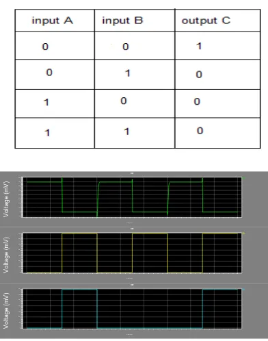
The condition for AND gate output to go high is all the input should be logic 1. If this condition is not met or if one of the inputs is logic 0 then output will always be in logic 0 states. With two NAND gate this basic gate is implemented as shown in Fig.4.the circuit current consumption is 34.13 pA and its power dissipation is only 23.88 pW which is the second lowest power consumption among all the gates. Operation table, Table IV shows the various input combination and its resultant output and the simulation result is also shown in Fig. 4 (a). To simulate the Gate, bit string (0111011101) and (0101010101) represent input A and B and at the output terminal C resultant bit (0101010101) is obtained.
[image:3.612.321.520.574.710.2]International Journal of Emerging Technology and Advanced Engineering
Website: www.ijetae.com (ISSN 2250-2459, ISO 9001:2008 Certified Journal, Volume 3, Issue 7, July 2013)
[image:4.612.66.545.64.436.2]79 Table IV
AND GATE OPERATION TABLE
0 .0 0 .5 1 .0 1 .5
T im e (u s )
0 1 00 2 00 3 00 4 00 5 00 6 00 7 00
V
o
lt
a
g
e
(m
V
)
v( d) and
0 .0 0 .5 1 .0 1 .5
T im e (u s )
0 1 00 2 00 3 00 4 00 5 00 6 00 7 00
V
o
lt
a
g
e
(m
V
)
v( b) and
0 .0 0 .5 1 .0 1 .5
T im e (u s )
0 1 00 2 00 3 00 4 00 5 00 6 00 7 00
V
o
lt
a
g
e
(m
V
)
v( a) and
Fig.4 (a) Simulation Result of AND Gate
(e). XOR GATE
Eight MOS transistor and two inverters are required to implement this gate shown in Fig 5. Power dissipation is also higher as the number of transistor is increased. For two input XOR gate, output is logic 0 when all the input are same else it will give logic 1 at the output as shown in the operation table, Table V. XOR gate dissipate a total power of 52.75 pW and its simulation result for two input combination of bit streams is also shown in Fig. 5 (a)
Fig.5 XOR GATE
Table V XOR GATE OPERATION TABLE
0 .0 0 .5 1 .0 1 .5 2 .0 2 .5 3 .0
T im e (u s )
0 1 00 2 00 3 00 4 00 5 00 6 00 7 00
V
o
lt
a
g
e
(m
V
)
v( c) xor run
0 .0 0 .5 1 .0 1 .5 2 .0 2 .5 3 .0
T im e (u s )
0 1 00 2 00 3 00 4 00 5 00 6 00 7 00
V
o
lt
a
g
e
(m
V
)
v( b) xor run
0 .0 0 .5 1 .0 1 .5 2 .0 2 .5 3 .0
T im e (u s )
0 1 00 2 00 3 00 4 00 5 00 6 00 7 00
V
o
lt
a
g
e
(m
V
)
v( a) xor run
Fig.5 (a) Simulation Result of XOR Gate
(f). XNOR
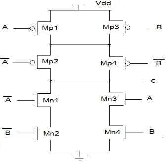
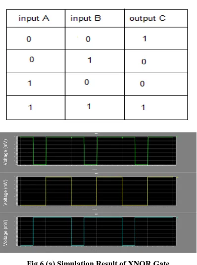
[image:4.612.342.543.125.397.2]This gate is the complement of XOR gate implementing with the same number of transistor as XOR Gate in Fig.6 but with the highest power dissipation of 84.63 pW due to different gate dimension. For two input gate if the inputs are same i.e. if input are (0,0) or (1,1) output is logic 1 else it will force its output to logic 0 as shown in simulation result Fig. 6 (a) along with its basic operation table in Table VI
[image:4.612.63.267.129.418.2] [image:4.612.355.536.527.705.2] [image:4.612.89.258.534.700.2]International Journal of Emerging Technology and Advanced Engineering
Website: www.ijetae.com (ISSN 2250-2459, ISO 9001:2008 Certified Journal, Volume 3, Issue 7, July 2013)
80 Table VI
XNOR GATE OPERATION TABLE
0 .0 0 .5 1 .0 1 .5 2 .0 2 .5 3 .0
T im e (u s )
0 1 00 2 00 3 00 4 00 5 00 6 00 7 00
V
o
lt
a
g
e
(m
V
)
v( c) xnor
0 .0 0 .5 1 .0 1 .5 2 .0 2 .5 3 .0
T im e (u s )
0 1 00 2 00 3 00 4 00 5 00 6 00 7 00
V
o
lt
a
g
e
(m
V
)
v( b) xnor
0 .0 0 .5 1 .0 1 .5 2 .0 2 .5 3 .0
T im e (u s )
0 1 00 2 00 3 00 4 00 5 00 6 00 7 00
V
o
lt
a
g
e
(m
V
)
v( a) xnor
Fig.6 (a) Simulation Result of XNOR Gate
[image:5.612.69.268.143.411.2] [image:5.612.73.265.465.652.2]The total circuit current n power dissipation in each of the logic gates is listed in the table below as shown in Table VII
Table VII
POWER DISSIPATION IN EACH GATE
IV. CONCLUSION
The technology use for implementing the MOS transistor is CMOS 180nm technology and the simulation toll is TANNER software. The power dissipation can thus be reduce as low as in the range of Pico-Watt by reducing
VDD as low as 0.7V along with scaling the size of length
and width of the MOS device. The first timing waveform in each simulation result represents the output result along with two input bits stream operating at 2MHz. The total current and power consumes by each of the logic family is
also tabled in Table VII. Circuit power dissipation mainly
depends upon the supply voltage. So by lowering the supply voltage and scaling the Gate’s dimension of the CMOS at the appropriate proportion, the total circuit power dissipation is thus lowered without affecting the overall circuit performance as shown in the entire simulation figure.
REFERENCES
[1 ] Reto Zimmermann and Wolfgang Fichtner, Fellow, IEE”
Low-Power Logic Styles: CMOS Versus PassTransistor Logic‖ IEEE
JOURNAL OF SOLID-STATE CIRCUITS, VOL. 32, NO. 7, JULY 1997
[2 ] Sreenivasa Rao Ijjada, B.Ramparamesh, Dr. V.Malleswara Rao”
Reduction of Power Dissipation in Logic Circuits” International Journal of Computer Applications (0975 – 8887)Volume 24– No.6, June 2011
[3 ] N. Geetha Rani1, N. Praveen Kumar2, Dr. B. Dr. B. Stephen Charles
3 Dr. P. Chandrasekhar Reddy 4 S.Md.Imran Ali 5 ―Design of
Near- Threshold CMOS Logic Gates” International Journal of VLSI design & Communication Systems (VLSICS) Vol.3, No.2, April 2012
[4 ] [4] Subodh Wairya1, Rajendra Kumar Nagaria2 and Sudarshan