N A N O E X P R E S S
Open Access
Fabrication and Photoluminescence Study
of Large-Area Ordered and Size-Controlled
GeSi Multi-quantum-well Nanopillar Arrays
Yuwen Jiang
1†, Shufan Huang
1†, Zhichao Zhu
2, Cheng Zeng
3, Yongliang Fan
1and Zuimin Jiang
1*Abstract
Large-area ordered GeSi multi-quantum-well nanopillar array (MQW-NPA) samples with different nanopillar lateral sizes (270, 120, and 70 nm) are fabricated by a cost-effective and scalable dry-etching process in combination with nanosphere lithography technique. A significant enhancement in photoluminescence (PL) intensity has been observed in the GeSi MQW-NPA samples compared with the as-grown GeSi MQW one. Nanopillar samples with different lateral sizes show different enhancements in PL intensity. The enhancements are analyzed quantitatively and attributed to three factors. One is the antireflection of the nanopillar structures. Another is an enhanced extraction in nanopillar arrays at the emission wavelength. Thirdly, the GeSi quantum wells in close proximity to the substrates would have more contribution to the PL than before etching. Our results show that all the three factors should be taken into account in designing and fabricating surface microstructures of GeSi MQW materials in order to improve their optical properties.
Keywords:GeSi, Quantum wells, Nanopillars, Photoluminescence PACS:78.67.-n, 61.72uf, 81.07.St, 62.23.Hj
Background
During the past decades, ordered semiconductor nano-structures, such as nanowires or nanopillar arrays, have drawn wide attention due to their promising applications in field-effect transistors [1, 2], light-emission devices [3], solar cells [4], novel electronic devices [5], lithium-ion battery [6], and so on. Si-based nanostructures are especially attractive because of their compatibility with current CMOS integrated circuits, however, their optical applications are largely limited due to the nature of their indirect bandgap and low quantum efficiency. Thus, several strategies have been proposed to resolve the low quantum efficiency of Si; among these, one is to inte-grate Si with other semiconductors like Ge to form heterostructures, such as Ge/Si quantum wells (QWs), quantum dot crystals, and nanowires (NWs) [7–11]. To
further improve the quantum efficiency of Si/Ge hetero-structures, different surface microstructures have also been proposed. The Choi group [12] observed a huge enhancement in the photoluminescence (PL) spectra from microdisk arrays of Si/Ge/Si SQW and proposed several mechanisms for the enhancement. One is the localization of excitons, which are spatially confined by the diameter of the microdisk. Another is the reduced nonradiative channels in the microdisk-patterned case. At the same time, they also pointed out that the real mechanisms for the PL enhancement were still not clear. The Chen group fabricated a randomly positioned SiGe/ Si multi-quantum-well (MQW) nanowall by using electron cyclotron resonance plasma etching on an as-grown SiGe/Si MQW, and the measured electrolumines-cence intensity of the SiGe/Si MQW nanowalls increased to about 1.5 times for the enhancement of emission light extraction [13]. Chen et al. also observed PL emission enhancement in size-uncontrollable Si/Ge superlattice pyramidal nanodots, which were fabricated by chemical selective etching through a self-assembled Ge QD mask [14]. Recently, Chang et al. successfully
* Correspondence:[email protected] †Equal contributors
1
State Key Laboratory of Surface Physics, Key Laboratory of Micro and Nano Photonic Structures (Ministry of Education), Collaborative Innovative Center of Advanced Microstructures, Department of Physics, Fudan University, Shanghai 200433, Peoples’Republic of China
Full list of author information is available at the end of the article
improving the PL emission properties of GeSi QWs are still not clear, especially in the quantitative analysis. Few studies have concerned how the lateral sizes of the nano-pillar affected the PL enhancement.
In this paper, large-area ordered and size-controlled GeSi MQW nanopillar arrays with different nanopillar lateral sizes were fabricated by a combination of nano-sphere lithography and dry etching. Compared to the as-grown GeSi MQWs, considerable enhancements in PL intensity have been observed in the GeSi MQW-NPA samples. The sample with the largest nanopillar size (270 nm) shows the most obvious enhancement. Three factors are analyzed quantitatively or qualitatively to ex-plain the enhancements. One factor is the antireflection of the nanopillar structures. The second one is the light extraction efficiency in nanopillar arrays at the emission wavelength. In addition, the GeSi quantum wells in close proximity to the substrates would have more contri-bution to the PL than before etching, due to a large penetration depth for the incident light, which is the third factor. In our study, we focus on the quantita-tive analyses for the PL enhancements in the GeSi multi-quantum-well nanopillar arrays (MQW-NPAs) with different lateral sizes. These analyses will be helpful in understanding the optical properties of other microstructured materials.
Methods
Ten periods of Ge (0.9 nm)/Si (12 nm) multi-quantum-well (MQW) samples were grown by a molecular-beam epitaxy (MBE) system (Riber EVA-32 ) on p-type Si wa-fers (<100> oriented, 0.01–0.02 Ω cm). The wafer was cleaned by a standard Radio Corporation of America (RCA) method and passivated by HF before loading into the MBE chamber. The deposition rates of Si and Ge were 0.625 and 0.1 Å/s, respectively. The wafer was pre-treated at 860 °C for 5 min. After that, a 30-nm-thick Si buffer layer was grown at 700 °C. The first 0.9-nm-thick Ge layer was deposited at 510 °C, and the first 12-nm-thick Si spacer layer was deposited at the temperature ramping from 510 to 560 °C. The other Ge quantum well layers and Si spacer layers were deposited at the same deposition temperature and with the same
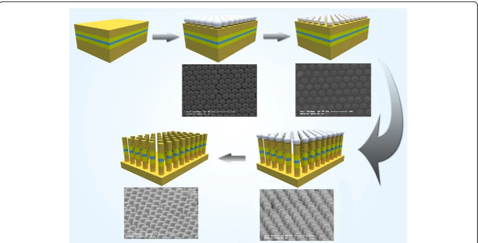
move the residual deionized water and other impurities. Next, the size of the PS was etched to a required diam-eter for the nanopatterned mask (~450, 350, and 250 nm) by oxygen plasma etching with a radio-frequency (RF) power of 30 W. After that, the sample was etched to nanopillar array structures with an ion-coupling plasma (ICP) process under the surface protec-tion by PSs. Finally, the remaining PSs were removed via another oxygen plasma-etching process.
Morphologies of GeSi MQW-NPAs were characterized by a field emission scanning electron microscopy (FE-SEM; XL30FEG, PHILIPS, Netherlands) equipped with an energy dispersive X-ray spectrometer (EDS) operating at 20 kV. Before SEM measurements, a 20-nm-thick Au layer was deposited onto the surface in order to get more distinct images. Hemispherical optical reflectance spectra of planar Si bulk and MQW-NPAs were col-lected in the wavelength range between 300 and 1100 nm (step, 5 nm) via a UV-Vis spectrometer. For PL measurements, the samples were placed in a closed-cycle helium cryostat with a temperature range from 16 K to room temperature, and a 488-nm line of Ar+ laser was used as the excitation source. The PL spectra were recorded by an extended InGaAs detector using the standard lock-in technique. Numerical simulations for the spatial distributions of optical field intensity were performed based on a rigorous coupled-wave analysis (RCWA) method and three-dimensional finite-difference-time-domain (FDTD) method.
Results and Discussion
of all the three samples are about 400 nm. In order to analyze the crystal quality of the samples after ICP etch-ing, Raman measurements were performed. As shown in Fig. 2d, for the as-grown MQW sample, the peaks at 230, 302, 417, and 437 cm−1 are assigned to Si(2TA)L,
Si(2TA)X, Si-Ge phonon mode, and Si-Si phonon (local)
modes, respectively. For the ICP-etched samples, both peaks of Ge(LO) and Si-Ge mode have a redshift com-pared to the as-grown MQW sample, which is mainly resulting from the compressive strain relaxation [13]. The
Fig. 1Scheme of the fabrication procedures of GeSi MQW-NPAs
[image:3.595.58.539.87.331.2] [image:3.595.56.539.454.712.2]Raman results prove that the crystalline quality of the ICP-etched samples was not damaged during the etching process.
Figure 3a shows the PL spectra of the as-grown MQW sample. The measurement was carried out at 16 K at an excitation power of 1 W. Two main peaks located at about 1.1 and 1.05 eV are attributed to transverse optical (TO) phonon-assisted recombination in the Si spacer layer and the doped Si substrate, respectively [16]. The broad weak peak at ~0.88 eV is attributed to the PL of GeSi MQWs. Figure 3b shows the PL spectra in the wavelength range from 0.72 to 0.93 eV. It can be seen that the PL intensity of GeSi MQW-NPA samples in-creased considerably compared with the as-grown MQW sample. We introduce a PL enhancement factor (PEF), PEF =INP/IQW, to quantitatively describe the PL
enhancement, where INP and IQW represent the
inte-grated intensities of the PL of the MQW-NPA samples and the as-grown sample, respectively. As shown in Table 1, the sample A has the largest enhancement, with a PEF of 2.61. Sample B and sample C have 2.25 and 1.55 PEF factors, respectively. The PEF increases with nanopillar lateral size. In addition, the peaks of the MQW-NPA samples show a small blueshift compared with the as-grown MQWs.
As mentioned above, there are several mechanisms proposed to explain the PL enhancement in the nano-patterned surface sample case. In the following, we will
discuss the enhancement in more detail and with quanti-tative calculations. Firstly, the possibility that the PL en-hancement mainly comes from the localization of excitons, i.e., quantum confinement, is ruled out, simply because of the two factors. One is the diameters of the nanopillars largely exceed the exciton Bohr radius of Ge and Si (~10 nm). The second is the MQW-NPA sample with a larger diameter has a large PEF, which is opposite to the attribution of localization of excitons.
Normally, a nanopatterned surface can be regarded as an antireflection layer, depending on the surface morph-ologies and wavelength of incident light. In our case, the large-area ordered GeSi MQW-NPAs can effectively re-duce the reflection of incident light, according to the previous results [17–19], which could increase the ab-sorption of incident light and result in PL enhancement. In order to verify the effect on the light trapping, both reflectance spectrum measurements and FDTD tions were carried out, as shown in Fig. 4. The simula-tion results are consistent with the experimental results, and the total hemispherical optical reflectance of GeSi MQW-NPA samples was all lower than that of the as-grown GeSi MQWs. Moreover, as shown in both Fig. 4a, b, it is clearly seen that the optical reflectance of the GeSi MQW-NPA samples decreases with increasing lat-eral size of the nanopillars at the incident light wave-length of 488 nm. Here, we define the absorption enhancement factor (AEF), AEF =ANP/AQW, whereANP
and AQW respectively represent the absorptances of the
MQW-NPA samples and the as-grown MQW sample at the wavelength of 488 nm, which are calculated by one minus reflectance. As shown in Table 1, sample A has the largest AEF and the AEF increases with increasing size of the nanopillars.
As shown in Table 1, the AEF values of the nanopillar samples are smaller than the corresponding values of the PEF, which implies that the increased light absorptance cannot be regarded as the only reason for the PL
[image:4.595.58.540.88.244.2]Fig. 3aPL spectra of as-grown GeSi MQWs.bPL spectra of as-grown GeSi MQWs and GeSi MQW-NPAs in a small scale
Table 1PEF, AEF, and EEF of GeSi MQWs and GeSi MQW-NPAs
PL enhancement factor (PEF)
Absorption enhancement factor (AEF)
Extraction enhancement factor (EEF)
As-grown MQWs
1 1 1
Sample A 2.61 1.55 2.66
Sample B 2.25 1.4 1.02
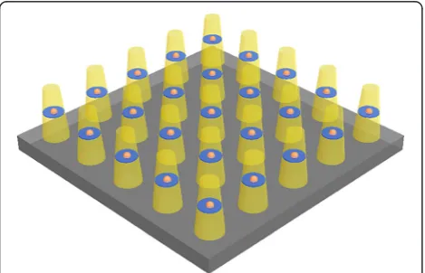
[image:4.595.57.290.636.731.2]enhancement of the nanopillar samples. So, we need to find the other reasons for the PL enhancement. It is well known that the photonic crystals could increase the ex-traction efficiency of lights [20]. Since the nanopillars in MQW-NPA samples are periodically arranged on the surfaces, photonic crystal effect should be taken into ac-count. FDTD simulations were performed at emission wavelengthλ= 1410 nm (0.88 eV) to further explore the reasons for the PL enhancement. In the simulations, the center of the nanopillar was taken as the coordinate ori-gin. An emission dipole was embedded in the QW plane (z= 0), as shown in Fig. 5. The method to calculate the extraction enhancement factor (EEF) can refer to Yue’s work [21]. At first, the extraction efficiency of a single dipole was simulated at different positions. Then, we took the average value on the extraction efficiency. Fi-nally, we define the EEF =ENP/EQW, whereENPandEQW
represent the extraction efficiencies of the MQW-NPA samples and the as-grown MQW sample, respectively. As shown in Table 1, the EEF of samples A, B, and C are found to be 2.66, 1.02, and 0.34, respectively.
It is noted that for sample C the EEF value is 0.34, and the AFE value times the EEF value equals 0.40, which is much smaller than the observed PEF value of 1.55. This implies that we need to find another possible reason to explain the PL enhancement for sample C.
As we know, the penetration depths of the 488-nm line of the Ar+ laser in Ge and Si are about 16 and 400 nm, respectively [15, 22]. For the as-grown GeSi MQW sample, most electron-hole (e-h) pairs are gener-ated in the top Si layer and the upper GeSi QW regions. The carriers generated in the top Si layer need to be transported to the QW regions and be captured, then the recombination of the e-h pairs in the QWs results in PL from the QWs. For the GeSi MQW-NPA samples, the effective penetration depth of light becomes larger, which results in two consequences. (1) More e-h pairs are generated at the QW regions and captured directly by QWs without carrier transport loss. (2) More e-h pairs are generated at and captured by the bottom GeSi QWs. These bottom QWs should have a better quality than the upper QWs and thus have a higher PL effi-ciency since the bottom QWs actually underwent a lon-ger annealing process during the growth [23, 24]. These two consequences lead to an enhancement in PL inten-sity for the MQW-NPA samples compared to the as-grown GeSi MQW sample.
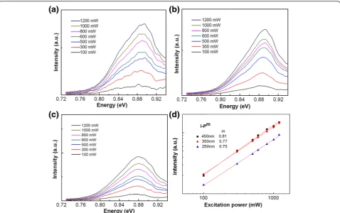
Figure 6a–c shows excitation power-dependent PL spectra of samples A, B, and C, respectively. Measure-ments were carried out at 16 K. Figure 6d shows the in-tegrated PL intensity as a function of the excitation power (I~Pm) for the three GeSi MQW-NPA samples. The coefficients m are found to be 0.75, 0.77, and 0.81 for the samples A, B, and C, respectively. This means the band alignment for the GeSi MQW-NPA samples is type II since themvalues are between 0.5 and 0.8, which are typical values for type II band alignment for the Ge/ Si heterostructures [25]. Besides, for the three samples, with increasing excitation power, the peak linewidth be-comes narrower and the peak energy has a blueshift,
Fig. 4aTotal hemispherical optical reflectance of GeSi MQWs and GeSi MQW-NPAs.bSimulated total hemispherical reflectance of GeSi MQW-NPAs
Fig. 5Model of the MQW-NPA samples for FDTD simulations. The
[image:5.595.59.539.88.223.2] [image:5.595.57.292.551.702.2]which is similar to the PL behavior of the GeSi quantum dot system [16]. For the type II band alignment, elec-trons and holes are resident in Si layers and GeSi quantum-well layers, respectively, being separated spatially. With increasing excitation power, more elec-trons and holes are generated, which make the band bending more severe in the case with type II band align-ment. At the same time, more electrons and holes will make the carriers fill higher energy level states. Both effects: band filling effect and band bending effect, would make the PL peak energy blueshift. In fact, with increasing excitation power, blueshifts in PL spectra have been observed in many GeSi systems with type II band alignment, which are also attributed to those two effects [26–28].
Conclusions
We successfully fabricate large-area ordered GeSi nano-pillar arrays with different lateral sizes (270, 120, and 70 nm) by a cost-effective nanosphere lithography tech-nique. Compared to the as-grown GeSi MQW sample, the GeSi MQW-NPA samples with different lateral sizes show different enhancements in PL intensity. The GeSi MQW-NPA sample with the largest nanopillar size shows the largest enhancement, which is as high as 2.61.
The enhancements are attributed to three factors, antire-flection of nanopillar structures, enhanced extraction ef-ficiency, and more contribution to the PL from bottom GeSi QWs. Three factors are analyzed quantitatively or qualitatively, and each plays an important role for the PL enhancement. Those analyses can help understand the optical properties of the MQWs of surface microstruc-tures as well as design surface microstrucmicrostruc-tures in order to improve their optical properties.
Abbreviations
AEF:absorption enhancement factor; EEF: emission enhancement factor; FDTD: finite-difference-time-domain; ICP: ion-coupling plasma;
MBE: molecular-beam epitaxy; MQW-NPAs: multi-quantum-well nanopillar arrays; MQWs: multi-quantum wells; PEF: PL enhancement factor; PL: photoluminescence.
Competing Interests
The authors declare that they have no competing interests.
Authors’Contributions
Y-WJ grew the GeSi MQW samples with the help of Y-LF and participated in the theoretical simulation. S-FH performed the PL and reflectance spectrum measurements. Y-WJ and S-FH interpreted the results and wrote the manuscript under the instruction of Z-MJ. Z-CZ performed the FDTD simulations. CZ carried out the ICP etching. Y-WJ and S-FH have equal contributions. All authors read and approved the final manuscript.
[image:6.595.59.538.87.387.2]Acknowledgements
This work was supported by special funds for the Major State Basic Research Project (Nos. 2011CB925601, 2013CB933303, and 2013CB632104) of China, and the Natural Science Foundation of China (NSFC) under Project Nos. 61274016, 11274072, 10974031, and 61177049.
Author details 1
State Key Laboratory of Surface Physics, Key Laboratory of Micro and Nano Photonic Structures (Ministry of Education), Collaborative Innovative Center of Advanced Microstructures, Department of Physics, Fudan University, Shanghai 200433, Peoples’Republic of China.2Shanghai Key Laboratory of
Special Artificial Microstructure Materials and Technology, School of Physics Science and Engineering, Tongji University, Shanghai 200092, Peoples’ Republic of China.3Wuhan National Laboratory for Optoelectronic, School of
Optoelectronic Science and Engineering, Hua Zhong University of Science and Technology, Wuhan 430074, Peoples’Republic of China.
Received: 24 November 2015 Accepted: 14 February 2016
References
1. Cui Y, Zhong Z, Wang D, Wang WU, Lieber CM (2003) High performance silicon nanowire field effect transistors. Nano Lett 3(2):149–52 2. Guo W, Zhang M, Banerjee A, Bhattacharya P (2010) Catalyst-free InGaN/
GaN nanowire light emitting diodes grown on (001) silicon by molecular beam epitaxy. Nano Lett 10(9):3355–9
3. Zheng G, Lu W, Jin S, Lieber CM (2004) Synthesis and fabrication of high-performancen-Type silicon nanowire transistors. Adv Mater 16(21):1890–3 4. Wang KL, Cha D, Liu J, Chen C (2007) Ge/Si self-assembled quantum dots
and their optoelectronic device applications. P IEEE 95(9):1866–83 5. Schmidt OG, Eberl K (2001) Self-assembled Ge/Si dots for faster field-effect
transistors. IEEE T Electron Dev 48(6):1175–9
6. Ge M, Rong J, Fang X, Zhou C (2012) Porous doped silicon nanowires for lithium ion battery anode with long cycle life. Nano Lett 12(5):2318–23 7. Abstreiter G, Brugger H, Wolf T, Jorke H, Herzog HJ (1985) Strain-induced
two-dimensional electron gas in selectively doped Si/SixGe1-x superlattices. Phys Rev Lett 54(22):2441–4
8. Arbet‐Engels V, Kallel M, Wang K (1991) Photoluminescence of hydrogenated SimGen superlattices. Appl Phys Lett 59(14):1705–7 9. Fukata N, Mitome M, Sekiguchi T, Bando Y, Kirkham M, Hong J-I et al. (2012)
Characterization of impurity doping and stress in Si/Ge and Ge/Si core–shell nanowires. ACS Nano 6(10):8887–95
10. Gruetzmacher D, Fromherz T, Dais C, Stangl J, Mueller E, Ekinci Y et al. (2007) Three-dimensional Si/Ge quantum dot crystals. Nano Lett 7(10):3150–6
11. Ma Y, Zhong Z, Lv Q, Zhou T, Yang X, Fan Y et al. (2012) Formation of coupled three-dimensional GeSi quantum dot crystals. Appl Phys Lett 100(15):153113
12. Choi S-H, Kim JN, Kim HY, Hong Y-K, Koo J-Y, Seok J et al. (2002) Enhancement of photoluminescence by microdisk formation from Si/Ge/Si single quantum wells. Appl Phys Lett 80(14):2520–2
13. Chen TT, Hsieh YP, Wei CM, Chen YF, Chen LC, Chen KH et al. (2008) Electroluminescence enhancement of SiGe/Si multiple quantum wells through nanowall structures. Nanotechnology 19(36):2618–24 14. Chen HC, Wang CW, Lee SW, Chen LJ (2006) Pyramid-shaped Si/Ge
superlattice quantum dots with enhanced photoluminescence properties. Adv Mater 18(3):367–70
15. Chang HT, Wu BL, Cheng SL, Tu L, Lee SW (2013) Uniform SiGe/Si quantum well nanorod and nanodot arrays fabricated using nanosphere lithography. Nanoscale Res Lett 8(31):349
16. Ma Y, Zhong Z, Lv Q, Qiu W, Wang X, Zhou T et al. (2013) Optical properties of coupled three-dimensional Ge quantum dot crystals. Opt Express 21(5):6053–60
17. Huang S, Zhang H, Wu Z, Kong D, Lin D, Fan Y et al. (2014) Large-area ordered p-type Si nanowire arrays as photocathode for highly efficient photoelectrochemical hydrogen generation. ACS Appl Mater Inter 6(15):12111–8
18. Huang Z, Wu Y, Fang H, Deng N, Ren T, Zhu J (2006) Large-scale Si1−xGex
quantum dot arrays fabricated by templated catalytic etching. Nanotechnology 17(5):1476
19. Wu Z, Wang Z, Wang S, Zhong Z (2014) Substantial influence on solar energy harnessing ability by geometries of ordered Si nanowire array. Nanoscale Res Lett 9(1):495
20. Wierer JJ, David A, Megens MM (2009) III-nitride photonic-crystal light-emitting diodes with high extraction efficiency. Nat Photonics 3(3):163–9 21. Yue Q, Li K, Kong F, Zhao J, Li W (2013) Analysis on the light extraction
efficiency of GaN-based nanowires light-emitting diodes. IEEE J Quantum Elect 49(8):697–704
22. Palik ED (1985) Handbook of optical constants of solids. Academic Press Handbook 33(1):189
23. Dashiell MW, Denker U, Müller C, Costantini G, Manzano C, Kern K et al. (2002) Photoluminescence of ultrasmall Ge quantum dots grown by molecular-beam epitaxy at low temperatures. Appl Phys Lett 80(7):1279–81 24. Fukatsu S, Usami N, Shiraki Y (1993) Luminescence from Si1−xGex/Si
quantum wells grown by Si molecular-beam epitaxy. J Vac Sci Technol B 11(3):895–8
25. Chen Y, Pan B, Nie T, Chen P, Lu F, Jiang Z et al. (2010) Enhanced photoluminescence due to lateral ordering of GeSi quantum dots on patterned Si (001) substrates. Nanotechnology 21(17):175701
26. Wan J, Jin GL, Jiang ZM, Luo YH, Liu JL, Wang KL (2001) Band alignments and photon-induced carrier transfer from wetting layers to Ge islands grown on Si(001). Appl Phys Lett 78(12):1763–5
27. Tao Z, Yang H, Zhong Z, Zhan N, Yan L, Lu F (2009) The studies of Ge quantum dots on strained Si0.7Ge0.3layer by photoluminescence and deep
level transient spectroscopy. Appl Surf Sci 255(6):3548–51
28. Baier T, Mantz U, Thonke K, Sauer R, Schäffler F, Herzog HJ (1994) Type-II band alignment in Si/Si1−xGexquantum wells from photoluminescence line
shifts due to optically induced band-bending effects: experiment and theory. Phys Rev B 50(20):15191–6
Submit your manuscript to a
journal and benefi t from:
7Convenient online submission
7Rigorous peer review
7Immediate publication on acceptance
7Open access: articles freely available online
7High visibility within the fi eld
7Retaining the copyright to your article