Abstract
The resistive switching characteristics of the Cu/SiOx/Pt structure (control sample) exhibited a direct correlation to humidity. The H2O vapor formed the Cu oxide at the Cu/SiOxinterface, and Cu ions were injected from the Cu oxide into the SiOxlayer, thus improving the resistive switching. However, the control sample demonstrated substantial switching dispersion in a vaporless environment. The CuxO layer in the Cu/CuxO/SiOx/Pt structure (CuxO sample) helped the dissolution of Cu ions from the Cu electrode into the SiOxlayer, enabling effective electrochemical resistive switching in a vaporless environment. The CuxO sample exhibited low switching dispersion and favorable endurance characteristics in a vaporless environment.
Keywords:CuxO; Resistive switching; SiOx PACS:73.50.-h; 73.40.Rw; 73.61.Ng
Background
Recently, resistive random access memory (RRAM) has attracted considerable interest because of its non-volatile resistance change in simple metal/insulator/metal struc-tures [1, 2]. Depending on the material group [3], device structure [4, 5], and defect status [6, 7], various switch-ing behaviors can be observed. The switchswitch-ing mecha-nisms are typically classified as either a valence change effect [8], a thermochemical effect [2, 9], or an electro-chemical effect [10, 11], whereby distinct surface effects can be attributed to various mechanisms [12, 13]. Ke et al. proposed that the oxygen concentration influences the redox reaction in ZnO resistive switching [12], and Tsuruoka et al. suggested that H2O vapor plays as an
es-sential role in the redox reaction of an electrochemical Cu/SiO2/Pt device [13, 14]. The effects of moisture on
Cu/SiO2/Pt and Cu/Ta2O5/Pt devices were different due
to different adsorption coefficients of water. H2O vapor
formed a Cu oxide interface between the Cu electrode and the oxide layer after the forming process and also enhanced Cu migration within the oxide layer. The H2O
vapor facilitates in the dissolution of Cu ions into the SiO2 layer, enabling effective resistive switching. The
Cu/SiO2/Pt device does not perform the resistive
switching without H2O vapor [13, 14]. However, there is
no H2O vapor within a packaged chip, and this is a
serious concern, because these devices are used in mem-ory applications.
In this study, a CuxO layer was inserted between the Cu
and SiOx layer to improve the electrochemical resistive
switching and minimize switching dispersion in a vapor-less environment.
Methods
A 20-nm-thick SiOx layer was deposited on a Pt-coated substrate (Pt/Ti/SiO2/Si) using radio frequency
sputter-ing at room temperature. Subsequently, a 200-nm-thick Cu electrode was deposited using a thermal evaporator at room temperature, to form the final Cu/SiOx/Pt struc-ture (control sample). The device area was 5 × 10⁻⁵cm2. To create the Cu/CuxO/SiOx/Pt structure (CuxO sample), an additional 1-nm CuxO layer was deposited on the SiOx layer by using a thermal evaporator at room temperature. The structures of the control sample and the CuxO sam-ple are illustrated in Fig. 1, respectively. X-ray photoelec-tron spectroscopy (XPS; PHI-5000, ULVAC-PHI) was used to analyze the composition of the CuxO layer. The electrical measurements were performed using an HP 4155B semiconductor parameter analyzer, and the mea-surements were taken in both air (60 % relative humidity) and N2 environments at room temperature. The bias
* Correspondence:[email protected]
Department of Electronic Engineering, National Kaohsiung University of Applied Sciences, No.415, Chien Kung Road, Kaohsiung 807, Taiwan
voltage was applied on the top electrode while the bottom electrode was grounded.
Results and Discussion
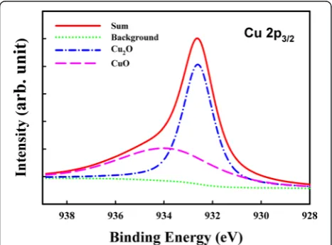
Figure 2 depicts the XPS Cu 2p3/2 spectra of the CuxO
layer. The detailed chemical structure information was extracted through deconvolution of Cu 2p3/2 peaks,
which showed a CuO peak locating at 934 eV and a Cu2O peak locating at 932.6 eV. The CuxO layer is the
mixture of CuO and Cu2O. Figure 3 shows the resistive
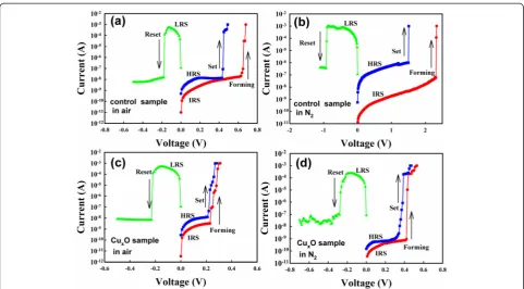
switching characteristics of the control and the CuxO samples in both air and N2 environments. A
positive-forming voltage was used to initialize the resistive switching; the resistance state was then switched from an initial resistance state (IRS) to a low resistance state (LRS). Following this transition, a negative Reset voltage was applied to switch from the LRS to a high resistance state (HRS). Subsequently, using a positive Set voltage, the HRS was switched back to a LRS. The device resist-ance can be reversibly switched between a LRS and a HRS by a Set voltage and a Reset voltage. Figure 3c, d illustrates the resistive switching characteristics of the CuxO sample in air and N2 environments, and the
behaviors were similar to those of the control sample in air. According to our previous study [15], device structure, and switching behavior, the resistive switchings of the con-trol sample in air and the CuxO sample in both
environ-ments are dominated by the electrochemical model with a Cu conducting filament. However, as shown in Fig. 3b, the control sample in the N2environment required
substan-tially higher operating voltages. The control sample in the N2environment also showed a reversible unipolar
switch-ing, and the temperature coefficient of LRS resistance was negative. Therefore, the switching mechanism should be the thermochemical effect with conducting filaments of oxygen-related defects.
Tsuruoka et al. proposed that a Cu/SiO2/Pt structure
ex-hibits no resistive switching in a vacuum or N2
environ-ment (no H2O vapor) because of the desorption of
residual water from the SiO2layer [13]. Because the
com-position of the SiOxfilm influences the switching
mechan-ism [16], the result of this study in N2 differed from the
result of Tsuruoka et al., which may be due to the dissimi-lar composition between SiOx and SiO2layers. Although
there was some difference between Tsuruoka’s study and our control sample in N2, these two samples both
per-formed unfavorably because of a lack of humidity and ex-hibited no electrochemical resistive switching. Because no copper oxide was formed at the Cu/SiOx(or SiO2)
inter-face of these two samples, no electrochemical resistive switching was observed. The Cu ion concentrations were calculated using the cyclic voltammetry (CV) method [17], and the results are presented in Fig. 4. The CV method is used to study the redox reaction of Cu within the device. The applied voltage swept to 0.15 V and then swept back until the current was zero. During this sweep-ing period, oxidized Cu ions were injected into the SiOx
thin film. The amount of Cu ions (Q) can be calculated, and then, Cu ion concentration (Cion) can be determined
by the formula Cion¼qNQA=V, where NA is Avogadro’s
number and V is the device volume. The CuxO sample
contained higher Cu ion concentrations than those in the control samples. In addition, the two samples contained larger Cu ion concentrations in air than in N2. Tsuruoka Fig. 1Illustrations of the sample structures.athe control sample andbthe CuxO sample
Fig. 2XPS of the CuxO layer. Cu 2p3/2XPS spectra of the CuxO layer
[image:2.595.59.539.89.206.2] [image:2.595.57.291.542.714.2]et al. proposed that H2O molecules would form a
hydrogen-bond network at grain boundaries in SiO2[13]
and thus had larger Cu ion concentration. Therefore, the humidity and CuxO layer both help the dissolution of Cu
ions into SiOxlayer. The electrochemical resistive
switch-ing has three rate-limitswitch-ing processes [13]: the Cu ionization at the Cu/SiOx interface, the migration of Cu
ions in the SiOx film, and the nucleation of Cu at the Pt
bottom electrode. In this study, the Cu nucleation at Pt
electrode would not the rate-limiting process. The control sample in N2had the lowest Cu ion concentrations, and it
cannot show an electrochemical resistive switching, which means that the Cu ionization at the Cu/SiOx interface is
the rate-limiting process in N2. Willis and Lang [18]
pro-posed the three possible mechanisms for the Cu ionization at the Cu/SiO2interface under a positive applied voltage:
the anodization-like process that Cu atoms are injected directly into the SiO2 layer by the dissolution reaction
Cu→Cuz++ze−, Cu ions injected into the SiO2from the
CuxO formed at the Cu/SiO2interface due to reduction of
the SiO2, and the chemical oxidation of Cu atoms at the
Cu/SiO2interface via H2O, O2, or out-gassing of the oxide
[13]. In this study, the Cu/SiOx/Pt cannot
electrochem-ically switch in N2. Therefore, the former two mechanisms
should be excluded.
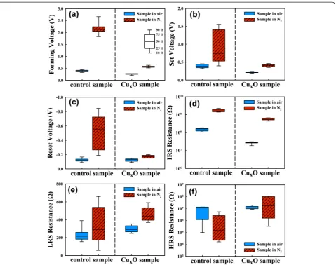
Figure 5a–c depicts the operating voltages of the two samples in both environments. The control sample in N2 exhibited the highest operating voltages because of
the lowest Cu ion concentration within the SiOx layer.
Both samples exhibited lower operating voltages in air, as the H2O vapor increased the Cu ion concentration in
the SiOx layer. Tappertzhofen et al. proposed that there
was no copper oxide at Cu/SiO2 interface before the
forming process, but the copper oxide was found after the forming process in air [14]. In addition, this electro-chemical oxidation was not observed in anhydrous atmosphere. We also fabricated a Ni (200 nm)/CuxO Fig. 3The resistive switching characteristics in different measurement environments.aThe control sample in air.bThe control sample in N2.cThe CuxO sample in air.dThe CuxO sample in N2
[image:3.595.57.539.87.353.2] [image:3.595.58.290.528.694.2](1 nm)/SiOx(20 nm)/Pt structure (not shown) which did
not have an electrochemical resistive switching. This means that the 1-nm CuxO interlayer did not provide
enough Cu ions to form Cu conducting filaments. Since the Cu electrode cannot be directly ionized to be Cu ions and a 1-nm CuxO interlayer does not provide
enough Cu ions to form Cu conducting filaments, the possible explanation is that the Cu metal is transformed into immediate states of Cu oxide via the CuxO layer
and then Cu ions can be injected from these immediate states by a positive electric field. Since the copper oxide cannot be electrochemically formed without a moisture environment, a CuxO layer in this study was deposited
between the Cu and SiOx layers to solve this issue. The
deposited CuxO layer also can help the dissolution of Cu
ions from the Cu electrode into the SiOx layer, thus
in-creasing the Cu ion concentration in the SiOxlayer. This
increase in the Cu ion concentration effectively reduced the forming and Set voltages. Figure 5d–f shows the
device resistances in both air and N2. The LRS
conduc-tion of the two samples in air and N2 exhibited ohmic
behavior. The LRS resistances were approximately deter-mined according to the current compliance during the Set process. The two samples exhibited lower LRS resis-tances in air, which may be due to an increased Cu ion concentration in the SiOx layer during the Set process
[8]. This increased concentration of Cu ions caused a formation of wider conduction filaments. The IRS and HRS conductions of the two samples were dominated by the Schottky emission (not shown). The two samples exhibited lower IRS resistances in air because of a lower Schottky barrier height. All switching parameters of the CuxO sample had larger variation in N2than in air. H2O
molecules would form a hydrogen-bond network at grain boundaries in SiO2[13] and thus enhanced Cu
mi-gration in the SiOx layer. Therefore, the CuxO sample
had larger Cu ion concentration in air than in N2. The
supply of Cu ions influenced the operating voltages and
Fig. 5The parameters of resistive switching of the two samples.aThe forming voltage.bThe Set voltage.cThe Reset voltage.dThe IRS voltage.eThe LRS resistance.fThe HRS resistance
[image:4.595.60.540.87.465.2]the stability to grow Cu conducting filaments. Hence, the CuxO sample had a lower Cu ion concentration in N2and
thus had larger variation in switching parameters.
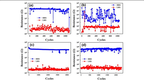
Figure 6 shows the endurance characteristics of the two samples in both environments. The control sample in N2exhibited the least favorable endurance
character-istics, because of its non-optimized thermochemical switching. Both of the samples exhibited a more favor-able endurance in air than in N2, which indicated that
H2O vapor increased the Cu ion concentration and thus
improved the resistive switching. In a packaged chip, the RRAM device must switch in an environment without H2O vapor. The CuxO sample demonstrated favorable
endurance for more than 2000 cycles in the N2
environ-ment, demonstrating that it is suitable for RRAM applications.
Conclusions
This study investigated the addition of a CuxO layer to a
Cu/SiOx/Pt structure for maintaining the
electrochem-ical resistive switching capabilities in a vaporless envir-onment. The Cu ionization at the Cu/SiOx interface is
the rate-limiting process for the electrochemical resistive switching in N2. Therefore, Cu/SiOx/Pt cannot have an
electrochemical resistive switching in N2. Therefore, in
the Cu/CuxO/SiOx/Pt structure, the CuxO layer helped
the dissolution of Cu ions from the Cu electrode into the SiOx layer, effectively minimizing the switching
dispersion. The Cu/CuxO/SiOx/Pt also exhibited
favor-able endurance characteristics in a vaporless environ-ment, demonstrating that it is suitable for practical applications.
Abbreviations
HRS:high resistance state; IRS: initial resistance state; LRS: low resistance state; RRAM: resistive random access memory; XPS: X-ray photoelectron spectroscopy.
Competing Interests
The authors declare that they have no competing interests.
Authors’Contributions
CYL designed the experiment, participated in the result analysis, and wrote the paper. ZYH prepared the devices and carried out the material analysis and electrical measurements. Both authors read and approved the final manuscript.
Authors’Information
CYL is an associate professor in the Department of Electronic Engineering, National Kaohsiung University of Applied Sciences, Taiwan. ZYH is a master student in the Department of Electronic Engineering, National Kaohsiung University of Applied Sciences, Taiwan.
Acknowledgements
The authors thank the National Science Council of R.O.C. for the financial supports under project No. NSC 102-2221-151-049 and the facility support from the National Nano Device Laboratories.
Received: 12 April 2015 Accepted: 5 July 2015
[image:5.595.59.537.89.355.2]References
1. Beck A, Bednorz JG, Gerber C, Rossel C, Widmer D. Reproducible switching effect in thin oxide films for memory applications. Appl Phys Lett. 2000;77:139–41.
2. Lee DY, Tsai TL, Tseng TY. Unipolar resistive switching behavior in Pt/HfO2/ TiN device with inserting ZrO2layer and its 1 diode-1 resistor characteristics. Appl Phys Lett. 2013;103:032905.
3. Pan F, Gao S, Chen C, Song C, Zeng F. Recent progress in resistive random access memories: materials, switching mechanisms, and performance. Mater Sci Eng R. 2014;83:1–59.
4. Tsai TM, Chang KC, Zhang R, Chang TC, Lou JC, Chen JH, et al. Performance and characteristics of double layer porous silicon oxide resistance random access memory. Appl Phys Lett. 2013;102:253509.
5. Huang CY, Jieng JH, Jang WY, Lin CH, Tseng TY. Improved resistive Switching characteristics by Al2O3layers inclusion in HfO2-based RRAM devices. ECS Solid State Lett. 2013;2:63–P65.
6. Chang KC, Tsai TM, Zhang R, Chang TC, Chen KH, Chen JH, et al. Electrical conduction mechanism of Zn:SiOxresistance random access memory with supercritical CO2fluid process. Appl Phys Lett. 2013;103:083509. 7. Lee CB, Kang BS, Benayad A, Lee MJ, Ahn SE, Kim KH, et al. Effects of metal
electrodes on the resistive memory switching property of NiO thin films. Appl Phys Lett. 2008;93:042115.
8. Zhou P, Yin M, Wan HJ, Lu HB, Tang TA, Lin YY. Role of TaON interface for CuxO resistive switching memory based on a combined model. Appl Phys Lett. 2009;94:053510.
9. Russo U, Ielmini D, Cagli C, Lacaita AL. Self-accelerated thermal dissolution model for reset programming in unipolar resistive-switching memory (RRAM) devices. IEEE Trans Electron Devices. 2009;56:193–200.
10. Schindler C, Staikov G, Waser R. Electrode kinetics of Cu–SiO2-based resistive switching cells: overcoming the voltage-time dilemma of electrochemical metallization memories. Appl Phys Lett. 2009;94:072109.
11. Valov I, Waser R, Jameson J, Kozicki MN. Electrochemical metallization memories—fundamentals, applications, prospects. Nanotechnol. 2011;22:254003.
12. Ke JJ, Liu ZJ, Kang CF, Lin SJ, He JH. Surface effect on resistive switching behaviors of ZnO. Appl Phys Lett. 2011;99:192106.
13. Tsuruoka T, Terabe K, Hasegawa T, Valov I, Waser R, Aono M. Effects of moisture on the switching characteristics of oxide-based, gapless-type atomic switches. Adv Funct Mater. 2012;22:70–7.
14. Tappertzhofen S, Valov I, Tsuruoka T, Hasegawa T, Waser R, Aono M. Generic relevance of counter charges for cation-based nanoscale resistive switching memories. ACS Nano. 2013;7:6396–402.
15. Liu CY, Sung PW. Different resistive switching characteristics of a Cu/SiO2/Pt structure. Jpn J Appl Phys. 2011;50:091101.
16. Wang Y, Chen K, Qian X, Fang Z, Li W, Xu J. The x dependent two kinds of resistive switching behaviors in SiOxfilms with different x component. Appl Phys Lett. 2014;104:012112.
17. Tappertzhofen S, Mundelein H, Valov I, Waser R. Nanoionic transport and electrochemical reactions in resistively switching silicon dioxide. Nanoscale. 2014;4:3040–3.
18. Willis BG, Lang DV. Oxidation mechanism of ionic transport of copper in SiO2dielectrics. Thin Solid Films. 2004;467:284–93.
Submit your manuscript to a
journal and benefi t from:
7Convenient online submission 7Rigorous peer review
7Immediate publication on acceptance 7Open access: articles freely available online 7High visibility within the fi eld
7Retaining the copyright to your article
Submit your next manuscript at 7 springeropen.com